Banked Microarchitectures for Complexity-Effective Superscalar
Microprocessors
by
Jessica Hui-Chun Tseng
Submitted to the Department of Electrical Engineering and Computer Science in partial fulfillment of the requirements for the degree of
Doctor of Philosophy at the
MASSACHUSETTS INSTITUTE OF TECHNOLOGY May 2006
@ Massachusetts Institute of Technology 2006. All rights reserved.
Author ... ...-.. -. r... v... , .... Depart of Electrical Engineering and Compi; cience
May 5, 2006 Certified by ... y . -. . -... Krste Asanovid Associate Professor Thesis Supervisor -r Accepted by ... (. ..
IMASSA
OFTELOGIBRAR
SE
M, ,
LIBRARIES
... .. ... .k ... ... ... Arthur C. Smith Chairman, Department Committee on Graduate StudentsA•CHIVES
Banked Microarchitectures for Complexity-Effective Superscalar Microprocessors by
Jessica Hui-Chun Tseng
Submitted to the Department of Electrical Engineering and Computer Science on May 5, 2006, in partial fulfillment of the
requirements for the degree of Doctor of Philosophy
Abstract
High performance superscalar microarchitectures exploit instruction-level parallelism (ILP) to improve pro-cessor performance by executing instructions out of program order and by speculating on branch instruc-tions. Monolithic centralized structures with global communications, including issue windows and register files, are used to buffer in-flight instructions and to maintain machine state. These structures scale poorly to greater issue widths and deeper pipelines, as they must support simultaneous global accesses from all active instructions. The lack of scalability is exacerbated in future technologies, which have increasing global interconnect delay and a much greater emphasis on reducing both switching and leakage power. However, these fully orthogonal structures are over-engineered for typical use. Banked microarchitectures that con-sist of multiple interleaved banks of fewer ported cells can significantly reduce power, area, and latency of these structures. Although banked structures exhibit a minor performance penalty, significant reductions in delay and power can potentially be used to increase clock rate and lead to more complexity-effective designs. There are two main contributions in this thesis. First, a speculative control scheme is proposed to simplify the complicated control logic that is involved in managing a less-ported banked register file for high-frequency superscalar processors. Second, the RingScalar architecture, a complexity-effective out-of-order superscalar microarchitecture, based on a ring topology of banked structures, is introduced and evaluated.
Thesis Supervisor: Krste Asanovid Title: Associate Professor
Acknowledgments
First, I like to thank my advisor Krste Asanovi6 for supporting me throughout this work and for his constant advice and encouragement. He is such a great inspiration to any student who is interested in computer architecture research. I treasure my learning experience under his invaluable guidance. I also like to thank Professor Arvind and Professor Srini Devadas for reading my thesis and sitting on my committee. I thank Professor Jacob White for his academic advice in pursuing my graduate study.
Thanks to Christine Chan, Abe McAllister, Godfrey Tan, Jaime Teevan, Doug De Couto, and Mark Hampton for their collaborations in various class projects. Thanks to Ronny Krashinsky and Mike Karcz-marek for TA'ing 6.823 with me. More thanks to Ken Barr, Chris Batten, Steve Gerding, Jae Lee, Rose Liu, Albert Ma, Heidi Pan, Michael Zhang, Seongmoo Heo, and Emmett Witchel for being the greatest teammates.
I thank Professor Dean Tullsen for providing and helping me with SMTSIM. I thank Xiaowei Shen for being my mentor when I was interning in IBM T. J. Watson Research Center. I thank Victor Zyuban for many interesting discussions in register file designs. I also thank Joel Emer for sharing his insightful experiences in microprocessor designs.
Thanks to Anne: McCarthy for helping me settle in when I first joined the group. Thanks to Michael Vezza for providing IT support that saved me a great deal of time. Many thanks to Mary McDavitt for all her administrative help, encouragements, and moral supports during the last few years of my graduate work. Thanks to all my friends who have made my life in MIT so enjoyable and memorable. Special thanks to Jing Song, Joy Cheng, and Carolyn Lee, for being such wonderful roommates and great friends during my study in MIT. I miss our late night snacks and conversations.
Funding for my graduate work came from a number of sources including NSF graduate fellowship, NSF CAREER award CCR-0093354, DARPA PAC/C award F30602-00-2-0562, CMI project 093-P-IRFT, DARPA HPCA/PERCS project W0133890 with IBM Corporation, and donations from Intel Corporation and Infineon Technologies.
Last but not less, I like to thank Mom, Dad, David, and Will for their endless love, patience, support, and encouragements. Most of all, thank you for sharing this journey and believing in me.
Contents
1 Introduction
1.1 Thesis Overview . . . .
2 Background and Motivation
2.1 Superscalar Microprocessors ... . 2.1.1 In-order vs. Out-of-order ...
2.1.2 Terminology ...
2.1.3 Out-of-order Execution Pipeline ... . 2.1.4 Register File ...
2.1.5 Instruction Issue Window . . . . 2.2 Clustered Architectures ...
2.3 Efficient Register File Designs . . . ... . . . 2.3.1 Less-ported Structures ... . .
2.3.2 Multibanked Microarchitecture . . . .
2.3.3 Register Caching ...
2.3.4 Asymmetric Structure . . . . 2.3.5 Content Awareness ...
2.3.6 Other Related Work on Reduced Complexity 2.4 Efficient Instruction Issue Window Designs ... .
2.4.1 Tag Elimination ... 2.4.2 Banked Configuration ... 2.4.3 Pipeline Window . ... ... ... ... ... Register ... . . . . . . . . . . • . •. . . . ° . . . . . . . Files . . .
2.4.4 Scoreboard Scheduler . . . . 2.4.5 Distributed Scheduler ... . . .
2.4.6 Other Related ...
2.5 Motivation for Banked Microarchitectures ...
3 Methodology 3.1 Simulation framework 3.1.1 Front-End Pipeli 3.1.2 Dynamic Instruc ne Stages tion Schedulin ... ...
. . . .
and Execution . .... . . .
. . . .
. . . . . . . . . . 3.1.3 Commit Stage3.1.4 Memory Instruction Modeling 3.1.5 Additional Modifications . . . 3.2 Benchmarks ...
3.2.1 Dynamic Instruction Profiling 3.3 Baseline Superscalar Processor . . . .
3.4 IPC Versus Performance . . . .
for Banked Regis
4.1 Register Bank Structure ...
4.2 Physical Characteristics ... .. 4.2.1 Regfile Layout ...
4.2.2 Regfile Area Comparison ... 4.2.3 Regfile Delay and Energy Evaluation 4.3 Control Logic ...
4.3.1 Speculative Pipeline Control Scheme 4.3.2 Repairing the Issue Window . . .. 4.3.3 Conservative Bypass-Skip ... 4.3.4 Read Sharing ...
4.4 Modeling Local Port Contention ... 4.4.1 Port Conflict Probability (PCP)
ter .. . . .. . . . .. . . . . . .. . . 49 ... 50 . . . . . 52 ... 52 . . . . . 53 . . . . . 54 ... 55 . . . . . 56 . . . . . 57 . . . . . 58 ... 59 . .. . . 60 .... ... ... ... ... .. 60 8
4 A Speculative Control Scheme File ... . . . ... . . . . . . ... . . . . . . . . . ... . . .
4.4.2 PCP Analysis ... 61
4.5 Simulation Results ... 62
4.5.1 Performance Sensitivity ... 62
4.5.2 Extending to SMT Architecture ... 64
4.5.3 In-order Superscalar ... .... .. ... 66
4.5.4 Correlation Among Accesses ... 67
4.6 Sum m ary . .... . ... .. .. ... ... .. . .. . .. . ... ... . . .. . . ... . 68
5 RingScalar: A Complexity-Effective Banked Architecture 71 5.1 RingScalar Microarchitecture ... ... 72
5.1.1 Architecture Overview ... 72
5.1.2 Register Renaming ... 74
5.1.3 IssueW indow ... 77
5.1.4 Banked Register File ... 79
5.1.5 Bypass Network ... 80
5.2 Operand Availability ... . 81
5.3 Evaluation .. ... .. .. .... ... ... .. . .. ... . ... . . .. . . ... 82
5.3.1 Resource Sizing ... 83
5.3.2 IPC Comparison ... 84
5.3.3 Regfile Read Port Optimization Effectiveness . ... . .. . . 85
5.3.4 Two-waiting Queues ... 87
5.4 Complexity Analysis ... . ... ... . 87
5.5 Sum m ary ... ... . .. ... ... .. . .. ... .. .. ... . ... . .. ... 90
6 Conclusion and Future Work 91 6.1 Summary of Contributions ... ... ... . 91
List of Figures
2-1 IPCs for single-issue in-order, four-way in-order, and four-way out-of-order superscalar
ma-chines.. . . . .. . . .. . . . 23
2-2 Microarchitectures of (a) single-issue in-order, (b) four-wa of-order superscalar machines. ... 2-3 Four-way out-of-order superscalar execution pipeline. .. 2-4 A 32x 32 regfile structure with two read-port and one writ( 2-5 2-6 2-7 2-8 2-9 2-10 2-11 2-12 2-13 Wakeup circuitry of a scheduler. ... Latch-based compacting instruction issue queue. Clustered architecture. ... Ring clustered architecture ... Multibanked regfile structure ... Banked issue queue organization ... Distributed FIFO structured issue window .... Reservation station style issue window design. .. A multibanked architecture design. ... .y in-order, and (c) four-way out-... 24 e-port. . ... 26 ... ... ... ... 27 . . . . . 28 ... ... ... ... . 29 ... ... ... ... 3 1 ... ... ... ... 33 .. ... ... ... . 36 . . . . . 38 . . . . . 38 . . . . . 39 3-1 Simulation framework . ...
3-2 IPCs for the baseline configuration... ...
4-1 An eight-read, four-write port register file implemented using four two-read, two-write port banks. The register file interconnect and bypass network are shown as distributed muxes
4-2 Area comparison of four different 64x 32b regfiles for a quad-issue processor. The clear regions represent the storage cells while the lighter shaded regions represent the overhead circuitry in each bank. The black shading at the bottom is the area required for the global bitline column circuitry. The medium-dark shading to the side is the area for address decoders. 53 4-3 Detail area breakdown of various 64x32b eight read-port and four write-port register file
designs. . . . ... 54 4-4 Detail breakdown of various 64 x 32b eight read-port and four write-port register file designs
in terms of (a) read access delay and (b) read energy consumption. . ... 56 4-5 Pipeline structures of processor with unified register file and processor with multibanked
register file. An additional cycle is added for multibanked register file for read port arbitra-tion and muxing. Read bank and write bank conflicts are also detected in this cycle. ... 57 4-6 Pipeline diagram shows repair operation after conflicts are detected. The wakeup tag search
path is used to clear ready bits of instructions that had a conflict causing them to be reissued two cycles later. Any intervening instruction issues are killed. . ... 58 4-7 Conservative bypass skip only avoids read port contentions when the value is bypassed from
the immediately preceding cycle ... 59
4-8 PCP for designs with (a) 16 banks with varying number of local ports and (b) varying number of banks with two local ports ... ... 62 4-9 IPCs for the 4-issue pipeline with register file of size 80. . ... 63 4-10 IPCs for (a) 1-Thread, (b) 2-Thread, and (c) 4-thread workloads. ... 66 4-11 Normalized IPC % for a four-way in-order machine with a 8B2R2WYY regfile. Results are
normalized to the IPC of a four-way in-order superscalar with a fully-ported regfile. ... . . 67
4-12 Conflict cycle comparison for (a) reads and (b) writes ... .. . 68
5-1 RingScalar core microarchitecture for a four-issue machine. The reorder buffer and the
memory queue are not shown ... 73
5-2 RingScalar rename and dispatch. The sub and and instructions were already in the window before the new dispatch group. ... ... . 74
5-3 RingScalar register renaming and column dispatch circuitry. Only the circuitry for srcl of
5-4 Wakeup circuitry. ... 78
5-5 Latch-based compacting instruction queues. . ... ... 79
5-6 Percentage distribution of zero-waiting, one-waiting, and two-waiting instructions. ... 81
5-7 Percentage distribution of last-arrival operand for two-waiting instructions. ... 82
5-8 Average IPC comparison for different regfile sizes. . ... ... 83
5-9 RingScalar average IPC sensitivity to instruction window size. . ... 84
5-10 IPC for 1 thread workload with a gshare branch predictor. . ... 84
5-11 IPC for 1 thread workload with a perfect branch predictor. . ... 85
5-12 Percentage of operands that do not compete for regfile read port due to conservative bypass-skipped optimization ... ... 86
5-13 Percentage of operands that do not compete for regfile read port due to read-sharing opti-m ization. . . .. . . . .. . .. . . . .. . . . ... 86
List of Tables
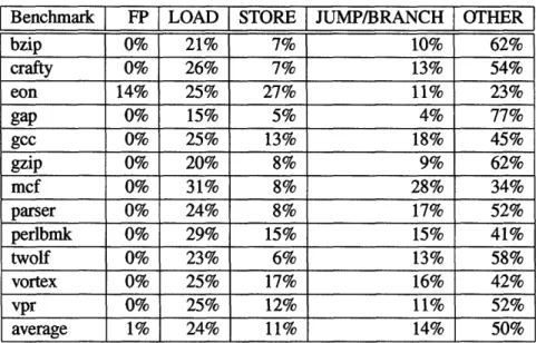
3.1 SPEC CINT2000 benchmarks description ... 45
3.2 The instruction distribution of SPEC CINT2000 benchmarks. . ... 46
3.3 Common simulation parameters. ... 47 4.1 Relative area of different 64 x 32-bit eight global read port and four global write port register
file designs. Packing is the number of local bit cells packed per global bit column. ... 54 4.2 Relative delay, energy, and leakage numbers of different 64x32-bit eight global read port
and four global write port register file designs. . ... ... 55
4.3 F(d,A,B,N) for various d values. ... ... 61
4.4 Normalized IPC % for a quad-issue machine with 80 physical registers. Configurations are labelled as (#banks)B(#local read ports)R(#local write ports)W(bypass skipped?)(read sharing?). Results are normalized to the IPC of the baseline case (unified with eight read
and four write ports) ... ... 63
4.5 Three workload categories ... 64
4.6 Heterogeneous multithreaded workloads. ... . . ... ... .. 65 5.1 Total complexity comparisons. Percentage results are normalized to the baseline
Chapter 1
Introduction
Conventional superscalar microarchitectures [Yea96, Kes99] employ monolithic centralized structures with global communications, including issue windows, register files, and bypass networks. These structures ;scale poorly to greater issue widths and deeper pipelines, as they must support simultaneous global accesses from all active instructions. They also scale poorly to future technologies, which have increasing global interconnect delay and a much greater emphasis on reducing both switching and leakage power.
To address this problem, decentralized clustered microarchitectures have been proposed [SBV95, KF96, FCJV97, RJSS97, AG05], where microarchitectures are divided into disjoint clusters each containing local instruction windows, register files, and functional units. However, clustering adds significant control logic complexity to map instructions to clusters and to manage communication of values between clusters. The :area and control complexity overhead of clustered architectures cannot be justified by the level of instruction parallelism in current applications [ZK01].
The other approach is to retain a centralized design but increase the efficiency of these fully orthogonal structures, which are over-engineered for typical usage. The challenge is in developing efficient microar-chitectures with simple pipeline control algorithms that allow smaller, less-orthogonal structures to attain good performance without adding excessive complexity. In this thesis, I argue that a complexity-effective superscalar microprocessor can be realized by constructing centralized structures from multiple interleaved banks of lesser ported cells.
The research conducted for this thesis builds upon earlier work in banked register files [WB96, CGVTOO, BDA01, PPV02], tag-elimination [EA02, KL03], and dependence-based scheduling [KF96, PJS97] and has
two main contributions:
* Developing a speculative control scheme for banked register files for high-frequency superscalar pro-cessors.
* Proposing a complexity-effective superscalar architecture that is based on a ring topology of banked microarchitectures.
1.1 Thesis Overview
This thesis consists of six chapters.Chapter 2 provides background and motivation for this work. It reviews conventional superscalar mi-croprocessors and shows that monolithic centralized structures with global communications such as register file, issue windows, and bypass network do not scale effectively with issue widths and deeper pipelines. Previous work in microarchitecture techniques that improve processor efficiency are examined, including clustered and banked architectures.
Chapter 3 describes the methodology and the baseline machine configuration used for this work. The SMTSIM simulator [Tul96] and the SPEC CINT2000 benchmark suite [HenOO] were used to evaluate the: performance of various banked microarchitectures and their control logic. Detailed models of register file, instruction window, and control logic were added to SMTSIM. A baseline machine configuration is chosen based on a preliminary analysis of the characteristics of the workload.
Chapter 4 examines energy-efficient banked multiported register file designs. Provided that the number of simultaneous accesses to any bank is less than the number of ports on each bank, a banked regfile can provide the aggregate bandwidth needs of a superscalar machine with significantly reduced area compared to a fully multiported regfile. Custom layouts of the regfile were used to determine the physical characteristic of various banking designs. Earlier banked schemes that required complex control logic with pipeline stalls would have likely limited the cycle time of a high-frequency design. I present a speculative control scheme suitable for a deeply pipelined high-frequency dynamically scheduled processor which avoids pipeline stalls. The performance impact of regfile port conflict mis-speculations are evaluated and verified with results from both a cycle-accurate simulator and an analytical model.
Chapter 5 applies the banking techniques to the instruction issue window and proposes a complexity-effective banked architecture, RingScalar. RingScalar builds an N-way superscalar from N columns, where each column contains a portion of the instruction window, a bank of the register file, and an ALU. By exploit-ing dependency-based schedulexploit-ing to place dependent instructions in adjacent columns, the bypass network is simplified into a ring connect, where a functional unit can only bypass values to the next functional unit. Furthermore, the fact that most instructions have only one outstanding operand when they enter the rename stage is exploited to use only one wakeup tag in the issue queue entries. This approach reduces the cost of broadcasting tag information across the window.
Chapter 2
Background and Motivation
Out-of-order superscalar microarchitectures provide high single-thread performance, but at a significant cost in terms of area and power. This overhead is due to large centralized structures with global communi-cations, including issue windows, register files, and bypass networks. This hardware dynamically extracts instruction-level parallelism (ILP) from a single instruction stream but scales poorly to greater issue widths and future technologies [PJS97], which have increasing global interconnect delay and rising leakage power. The advent of chip-scale multiprocessors, which integrate multiple cores per die, provides additional mo-tivation to improve the area and power efficiency of each core. In this chapter, I provide an overview of superscalar processors and related microarchitecture techniques. Then, I argue that banked microarchitec-tures merit investigation for their high area and power efficiency which results in a more complexity-effective machine.
Section 2.1 reviews the basic concepts of a superscalar microprocessor and its major components. High performance superscalar designs raise the overall instruction thoughput by issuing multiple instructions in parallel and executing instructions out of program order. The pipeline structure of an out-of-order super-scalar processor is illustrated and terminology is defined. I identify the reasons why orthogonal structures such as register files and instruction issue window are difficult to scale.
Section 2.2 discusses an alternative microarchitecture style, clustering, which aims to support greater issue widths at higher frequencies. Clustered architectures attempt to scale to larger issue widths by splitting the microarchitecture into distributed clusters, each containing a subset of register file, issue queue, and functional units [SBV95, KF96, FCJV97, RJSS97]. However, such schemes require complex control logic
to map instructions to clusters and to handle intercluster dependencies. Also, clustered designs tend to be less area efficient as they typically have low utilization of the aggregate resources [RF98].
Section 2.3 and Section 2.4 examine previous research in microarchitecture techniques that alleviate the scalability and efficiency problem of register files and instruction windows. Section 2.5 summarizes the main arguments made in this chapter.
2.1 Superscalar Microprocessors
Superscalar microprocessors started appearing in the late 1980s and early 1990s with the increasing popu-larity of RISC processors and the growing availability of transistor resources. Recent commercial general-propose processors such as Silicon Graphics's MIPS R10000 [Yea96], Digital's 21264 Alpha [Kes99]1, IBM's Power4 [TDF+01], Intel's P6-based processors, the Pentium 4 [HSU+01], as well as AMD's Athlon [AMD99] and Optero [KMAC03] are all superscalar processors.
2.1.1 In-order vs. Out-of-order
Superscalar microarchitectures increase processor performance by issuing multiple instructions simultane-ously to exploit the instruction-level parallelism (ILP) present in applications. A processor that can execute N instructions in parallel is an N-way machine. The ability to dynamically issue varying numbers of in-structions per clock cycle differentiates the superscalar from the VLIW (very long instruction word) design. In a VLIW design, the compiler schedules instructions statically. An in-order superscalar issues instructions dynamically depending on the dynamic detection of hazards, but always in program order. Out-of-order de-signs issue instructions potentially out of program order. Out-of-order execution machines require additional hardware to manage the precise architectural state of in-flight instructions, but reduce processor stalls from data dependencies. For example, in an in-order core, the pipeline stalls when the next waiting instruction is the consumer of data that is not yet available. In contrast, out-of-order processors perform future work by issuing other instructions that do not have an outstanding data dependency into the pipeline.
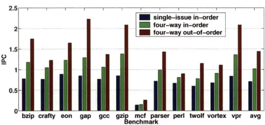
To evaluate the performance benefits of superscalar, Figure 2-1 shows the Instruction-committed-per-cycle (IPC) comparisons of different machines across the SPEC2000 CINT benchmark suite by using the methodology described in the next chapter. The simulated data indicates an approximately 40% improve-ment from a single-issue to a quad-issue in-order machine and another 40% improveimprove-ment from a four-way
C.)
M
bzip crafty eon gap gcc gzip mct parser perl twolT vortex vpr avg Benchmark
Figure 2-1: IPCs for single-issue in-order, four-way in-order, and four-way out-of-order superscalar ma-chines.
in-order to a four-way out-of-order superscalar machine.
However, Figure 2-2 shows that as the issue width quadruples, demand on the number of register file port increases by a factor of four and the bypass network grows substantially. For out-of-order superscalars, the number of register file entries must increase to support removal of artificial data dependencies by register renaming. An instruction issue window is also required to manage and schedule in-flight instructions out of program order. These highly centralized and orthogonal structures such as the register file, instruction issue window, and bypass network are typically very inefficient. Therefore, the focus of this thesis is finding tech-niques to improve the efficiency of high performance out-of-order superscalar processors, while retaining their performance advantages.
2.1.2 Terminology
Throughout the thesis, the following terminology will be used to describe dynamically scheduled superscalar execution cores.
* Fetch is the act of retrieving instructions from the instruction cache. * Decode is the process of decoding instruction opcodes and operands.
* Rename is the act of mapping an instruction's architectural registers to the physical registers.
etch Uni Decoder
(a) (b)
Figure 2-2: Microarchitectures of (a) single-issue in-order, (b) four-way in-order, and (c) four-way out-of-order superscalar machines.
* Dispatch is the process of moving the renamed instructions into the scheduling hardware, such as an instruction issue window.
* Issue is the process of sending ready instructions from the instruction issue window into the execution
units.
* Write Back is the act of writing results back to the physical register file. * Complete is the act of instructions leaving the pipeline after write back.
* Commit is the process of retiring completed instructions. The commit logic updates the architectural
state and releases resources such as entries in the reorder buffer (ROB), memory queue, and register file.
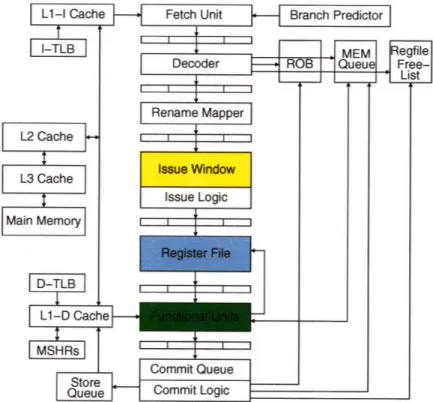
2.1.3 Out-of-order Execution Pipeline
A superscalar processor builds on a logically pipelined design, where each pipeline stage is in charge of one
of multiple tasks that are needed to complete each instruction. Figure 2-3 shows an example of a four-way out-of-order superscalar processor execution pipeline structure. Instructions are first fetched, decoded, and renamed. Instructions are then dispatched to the issue window and wait until both operands are available. The instruction issue window pipeline stage contains the critical wakeup-select loop [PJS97], where the wakeup phase is used to update operand readiness and the select phase picks a subset of the ready instructions
Fetch Unit
Decoder
--Feotch
oc l
ssue
ReadI
I
Fetch I Decode Rename Waup soec Bypass I Execute Writebac, Commit
Figure 2-3: Four-way out-of-order superscalar execution pipeline.
to issue. Once a single-cycle instruction is selected, its result tag is immediately broadcast to the instruction issue window in the next wakeup phase to allow back-to-back issue of dependent instructions, even though the selected instruction will not produce its result for several cycles. Before execution, register values are read from either the register file or the bypass network. After execution in the functional units, the results are written back to the register file and the instruction is committed in program order to maintain precise architectural state.
2.1.4 Register File
The multiported register file, or regfile, provides buffered communication of register values between pro-ducer and consumer instructions. With the deeper pipeline speculation and higher instruction-level paral-lelism (ILP) of more aggressive out-of-order superscalar processor designs, both the number of ports and the number of required registers increase. These increased requirements cause the area of a conventional mul-tiported regfile to grow more than quadratically with issue width [ZK98]. The trend towards simultaneous multithreading (SMT) [TEL95] further increases register count as separate architectural registers are needed for each thread. For example, the proposed eight-issue Alpha 21464 design had a regfile that occupied over
five times the area of the 64 KB primary data cache [Pre02].
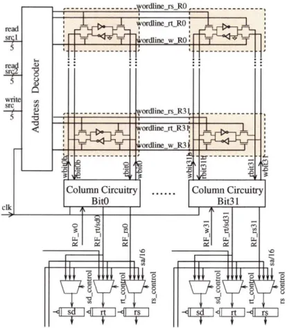
A register file is composed of SRAM like storage cells, address decoders, wordline drivers, column circuitry, multiplexing circuitry, and interconnects [ZK98, RDK+00, SJO1, BPN03]. Figure 2-4 shows a
32x 32-bit regfile with two single-ended read ports and one differential write port. The storage array is the main component and the cell size is constrained by the number of wires (bitline and wordlines) and the cross-coupled inverters. We can express the area of a multiported storage cell with single-ended reads and differential writes in a closed form, Equation 2.1. hi,, is the height of the coupled-inverters layout, win, is the width of the coupled-inverter layout, W is each wire-track space, Nr is the number of read ports, and
0
Figure 2-4: A 32x32 regfile structure with two read-port and one write-port.
areastorage = (hinv + W(Nr + N,)) x (winv + WNr + 2WNw) (2.1)
Both Figure 2-4 and Equation 2.1 indicate that the area of a conventional regfile increases super-linearly with the number of ports. For this reason, many architects have explored alternative designs for implement-ing a large and fast multiported register file.
One approach, used in the Alpha 21264 [Kes99] and 21464 [Pre02] designs, divides the functional units among two clusters and provides a copy of all registers in each cluster. This design halves the number of read ports required on each copy of the regfile, but requires the same number of write ports on both regfiles to allow values produced in one cluster to be made available in the second cluster. This approach isn't used to reduce area but to reduce read latency.
2.1.5 Instruction Issue Window
The instruction issue window or issue queue is where instructions wait to be scheduled to an appropriate execution unit. The issue window dynamically schedules instructions into the pipeline to exploit instruction-level parallelism to improve processor performance. Because the critical wakeup-select loop is part of the instruction issue window and its timing usually helps determine a processor's clock frequency, it is hard to scale this structure to greater issue widths [PJS97]. Moreover, studies have shown that the scheduler logic consumes a large portion of a processor's power (e.g. around 18% of total chip power of the Alpha 21264 [EA02]).
There are several styles in implementing a dynamic scheduler, but most designs employ a wakeup circuit to check the read-after-write data hazard and a select arbiter to choose instructions for issue. One approach is to store the direct source tags of each waiting instruction and dynamically update its readiness by matching the source tags to the result tags of issued instructions. As shown in Figure 2-5, each result tag passes through one of N wakeup ports and is driven across the entire window, with each entry having two comparators, leading to a fanout of 2E, where E is the number of entries. The direct source-tag scheduler requires
N [log2(X)1 wires to broadcast N result tags each cycle, where X is the number of regfile entries, and
a total of E x 2N [log2 (X)] bit-comparators. This scheme is shown to scale well with larger number of
registers but not with greater issue width.
wakeup ports
Figure 2-5: Wakeup circuitry of a scheduler.
Another variation of the direct source-tag approach is to one-hot encode the source tags as in the Alpha 21264 [FF98] processor. Each entry of the issue queue contains as many number of bits as the number of physical regfile entries, X. This bit array represents the data dependencies of each instruction and is the logical OR of two one-hot encoded sources. Again, the scheduler updates the readiness of instructions by matching the source field to destination registers of issued instructions each cycle. To reduce the number of wakeup ports, result tags (one-hot encoded) of issued instructions are ORed together. Since there is only
Figure 2-6: Latch-based compacting instruction issue queue.
one set of comparators for the source field, fanout for the wakeup port is also reduced from 2E to E. The one-hot encoding scheme requires only a single wakeup port but a larger storage array for issue window (
E x X instead of E x 2 log2(X)]). This design requires X wires to signal data completion and a total of EX bit-comparators.
The size of an issue window that uses one-hot encoding grows linearly with the size of regfile and becomes impractical for designs with a large number of registers. To improve the efficiency, Intel's Pentium 4 processor [HSU+01] stores the instruction dependencies in terms of one-hot encoded scheduler entry numbers instead of register numbers. The issue window is organized as a E x E bit matrix. As instructions are issued, they send the one-hot encoding that correspond to their issue queue entry numbers. This scheme requires E number of wires with a fanout of E to broadcast the entry numbers of issued instructions and a total of E2 bit-comparators. The complexity reductions of the scheduler, however, comes at the cost of an additional future-file like structure and the control logic that maps the architectural register numbers to
scheduler entry numbers.
Many issue queue designs keep instructions in age-order because it simplifies pipeline cleanup after exceptions or branch mispredictions and can improve performance over randomly assigned order. Figure 2-6 shows a latch-based compacting instruction queue design where the fixed-priority select arbiter picks the oldest ready instruction for issue. The age ordering of instructions is preserved by compacting out a
Figure 2-7: Clustered architecture.
completed instruction from the window, each entry below the hole retains its value, each entry at or above the hole copies the entry immediately above to squeeze out the hole, while the previous highest entry copies from the dispatch port if there's a new dispatch. Each entry has a single input port which is connected to a 2N fan-in mux, feeding from N dispatch ports and output ports of entries above. The dispatch ports are used to move the newly decoded instruction into the issue window. Also, each entry has one output port with a fanout of 2N, N to issue ports and N to input port of entries below. After instructions are selected, they are sent to the issue ports for further pipeline execution. The wide input mux and the large fanout of latch-based compacting issue queues makes it hard to scale to greater issue width.
Dynamic instruction schedulers are a central component in superscalar microprocessors and have re-ceived much attention in the literature [PJS97, BAB+02, RBR02, PKE+03]. Previous techniques that try to prevent the scheduler from becoming the critical path will be reviewed and discussed in Section 2.4.
2.2
Clustered Architectures
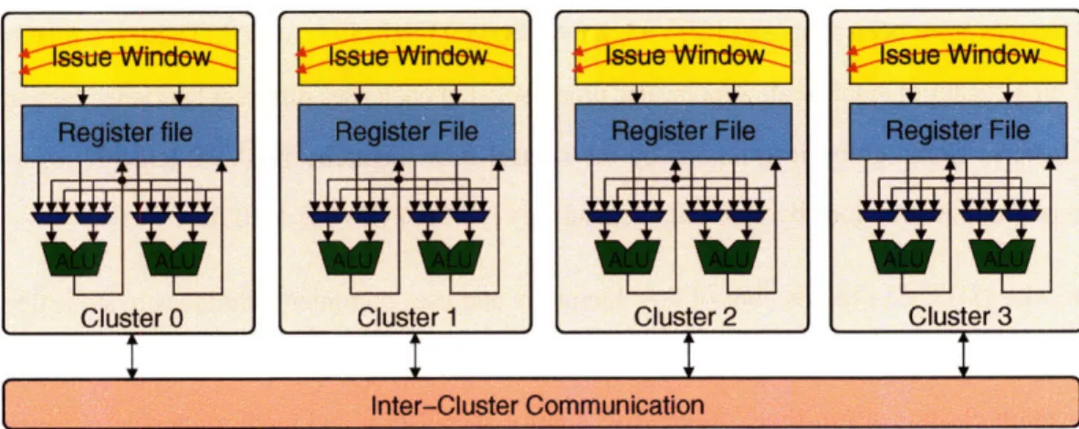
Clustered architectures divide the microarchitecture into disjoint clusters each containing local issue win-dows, register files, and functional units as shown in Figure 2-7. Inter-cluster communication is required when a value is needed from a different cluster. Clustering has the potential to scale with larger issue widths aan d at high clock frequencies but its performance can be affected by poor workload balancing and high inter-cluster communication penalties. Therefore, a critical matter in the design of such systems is the heuristics used to map instructions to clusters.
clustered designs have been proposed [SBV95, KF96, FCJV97, RJSS97, AGO5]. These microarchitectures are based on a cluster of small-scale superscalar processors but each uses different heuristics to map instruc-tions to clusters. Some group instrucinstruc-tions by the control flow hierarchy [SBV95, RJSS97] of a program while others group instructions by their data dependency [KF96, FCJV97, AG05].
Multiscalar [SBV95] exploits control flow hierarchy and uses compiler techniques to statically divide: a single program into a collection of tasks. Each task is then dynamically scheduled and assigned to one of many execution clusters at run-time. Aggressive control speculation and memory dependence speculation are implemented to allow parallel execution of multiple tasks. To maintain a sequential appearance, each task is retired in program order. This scheme requires extensive modification to the compiler and the performance depends heavily on the ability to execute tasks in parallel. On the other hand, Trace processors [RJSS97] are software invisible and build traces dynamically as the program executes. This approach, however, requires a large centralized cache to store the traces and the algorithm used to delineate traces strongly influences the overall performance. Both Multiscalar and Trace processors attempt to reduce inter-cluster communication by localizing program segments to an individual cluster but rely largely on control and value predictions for parallel execution.
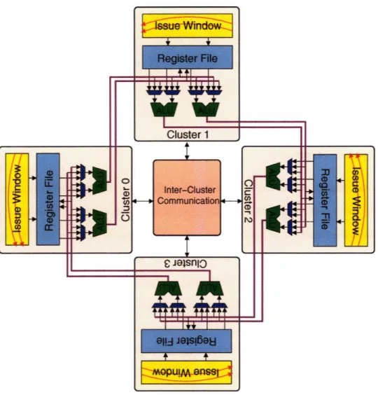
Data dependencies dictate the amount of communication between instructions. PEWs [KF96] and Mul-ticluster [FCJV97] assigns dependent instructions to the same cluster as much as possible to minimize inter-cluster communication and these assignments are determined at decode time. The performance is com-parable to a centralized design but decreases as the number of clusters increases. This is because such an algorithm has poor load balancing and cannot effectively utilize a large number of clusters. Multicluster sug-gests the possibilities of using complier techniques to increase utilization by performing code optimization and code scheduling. Instead, Abella and Gonzalez [AG05] proposed a scheme that inherently distributes the workload across all the clusters by placing consumer instructions in the cluster next to the cluster that contains the producer instructions. To minimize the cost of such next-neighbor cluster communication, the processor is laid out in a ring configuration so that the results of a cluster can be forwarded to the neighbor cluster with a very short latency as shown in Figure 2-8. Each partition of the register file can be read only from its cluster but can be written only from the previous neighboring cluster. Nevertheless, this design still requires long latency inter-cluster communications to move missing operands to appropriate clusters. I use a variant of this ring topology in the context of a centralized microarchitecture to reduce complexity.
[F
ii
Figure 2-8: Ring clustered architecture.
Clustered architectures have the potential to scale to larger issue widths by splitting the microarchitecture into distributed clusters. However, the primary disadvantages are the complexity of inter-cluster control logic and the complexity of mapping instructions to clusters. Clustered designs also require additional area to achieve performance similar to a centralized architecture for moderate size cores [ZK01]. Since our goal is to build a reduced complexity medium-size core, rather than an aggregation of multiple medium-sized cores to build a large core, the banking approach is a more suitable alternative.
2.3 Efficient Register File Designs
A variety of techniques have been proposed to reduce the complexity of a multiported regfile by exploring
different types of register access behaviors. For example, it is well known that a conventional regfile is
I1
II
=: :;
over-engineered for typical usage. Many data values are sourced from the bypass network, leaving regfile read ports underutilized [WB96, CGVTOO, BDA01, PPV02, TA03]. This motivates the designs of less-ported [PPV02, KM03] and multibanked regfiles [WB96, BDA01]. Additionally, localities in access and localities in value have been exploited to design hierarchical and simplified regfile structures [CGVT00. BTMEO2, JRB+98, BS03, AF03].
2.3.1 Less-ported Structures
Provided that the number of simultaneous accesses to regfile is less than the number of ports, the number of regfile ports can be reduced and still meet the aggregate bandwidth needs of a superscalar machine with savings in area, access latency, and power. Many authors have observed that over 60% of source operands are sourced from the bypass network and Park et al. [PPV02] proposed a bypass-hint scheme that reduces register read port contention. However, this bypass-hint is optimistic and can be incorrect. Pipeline stalls are required when read ports are oversubscribed but such stalls are difficult to implement in a high frequency pipeline without compromising cycle time. It is also observed that in over 50% cycles, all read ports and write ports are idle [HBHA02]. Kim et al. [KM03] recommend pre-fetching operands and adding delayed write-back queues to smooth out the burst behavior, so that a less-ported regfile can be used to provide the aggregate bandwidth, but this adds the cost of extending the bypass network. Nevertheless, both these proposals add complexity to the already timing critical wakeup-select loop, because the select logic still has to select no more instruction than the number of available read ports after considering the bypass hint bits [PPV02] or the prefetch flags [KM03].
2.3.2 Multibanked Microarchitecture
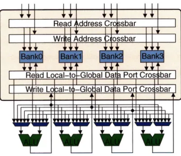
Similar performance can be reached with even fewer ports on each storage cell if the regfile is built from multiple interleaved banks [WB96, BDA01] (Figure 2-9). Such multibanked register file designs have been shown to provide sufficient bandwidth for a superscalar machine with significantly reduced area compared to a fully multiported regfile [WB96, BDA01]. The challenge with this approach is managing the complexity and added latency of the control logic needed to handle read and write bank conflicts and the mapping of register ports to functional units. Previous designs all have complex control structures that would likely limit
I II III III
d ddress Crossbar SAddress (ossbar
Figure 2-9: Multibanked regfile structure.
Wallace [WB96] describes a banking scheme that uses the bypass network to reduce unnecessary read port contention but no description of the bypass check or read conflict resolution logic is given. Also, write conflicts are handled by delaying physical register allocation until writeback, at which point registers are mapped to non-conflicting banks. The primary motivation for this delayed allocation was to limit the size of the physical register file, but this can lead to a deadlock situation requiring a complex recovery scheme [WB96].
The scheme presented in [BDA01] handles read bank conflicts by only scheduling groups of instructions without conflicts. This reduces the IPC penalty but adds significant logic into the critical wakeup-select loop. The authors also assume that bypassability can be determined during wakeup, but do not detail the mechanism used [BDA01]. A design with single-ported read banks is evaluated. However, this requires more complex issue logic to allow instructions where both operands originate from the same bank to be issued across two successive bank read cycles. Also, write port conflicts are handled by buffering conflicting writes, which increases the size of the bypass network. Functional unit pipelines must also be stalled when
the write buffers are full.
2.3.3 Register Caching
Localities of access have been used to design cache structures and can be extended to regfile designs. In [CGVTOO, BTME02], registers are cached to reduce average access latency. The disadvantage of
reg-ister caching is that it can add considerable control complexity to an architecture, as regreg-ister caches have much worse locality than conventional data caches and determining the appropriate values to cache is non-trivial. Register caching is motivated by the increasing access penalty of conventional multiported structures as port counts and register counts increase. Multibanking counteracts this increase and reduces total area, independent of the presence of exploitable localities.
2.3.4 Asymmetric Structure
As an alternative to less-ported storage cells to reduce the array size, an asymmetrically ported register file structure is proposed in [AF03] to decrease the wordline load. The author explores the fact that many of the register values are small and require only a small number of bits for representation to reduce the number of ports required for the most significant bits. The most significant bits of a regfile are less ported while the rest are fully ported. Again, this scheme involves additional complexity for the select logic and extra hardware that only reduces the wordline load. This asymmetric regfile structure still has problems with the scalability of the number of registers and the number of ports for the less significant bits.
2.3.5 Content Awareness
Clustering and banking approaches enable the implementations of regfiles with a large number of registers.. Alternatively, localities of register values have been used to design content-aware register files to reduce the number of registers required [JRB+98, BS03]. Both Jourdan [JRB+98] and Balakrishnan [BS03] propose a regfile design that only allocates a single physical register for each unique value. This scheme reduces the number of required physical registers by eliminating value duplication. However, reusing a physical register for different logical registers necessitates a large amount of additional hardware and complicated control logic in both the critical wakeup-select loop and regfile write backs.
2.3.6 Other Related Work on Reduced Complexity Register Files
The aforementioned work has focused on the design of a high bandwidth register file for dynamically sched-uled superscalar processors with a single logical register file. Other work has examined the use of partitioned register files made visible to software. The SPARC architecture [WG94] has overlapping register windows where software explicitly switches between sets of registers. In-order superscalar implementations of the
UltraSPARC exploit the fact that only one register window is visible to implement a dense multiported structure [TJS95]. Clustered VLIW machines make the presence of multiple register file banks visible to software, and the compiler is responsible for mapping instructions to clusters [Fis83]. Vector machines have also long been designed with interleaved register file banks that exploit the regular access patterns of vector instructions to provide high bandwidth with few conflicts [Cor89, DEC90].
2.4 Efficient Instruction Issue Window Designs
Many researchers identify the issue window's wakeup and select logic as likely one of the most critical timing and energy bottlenecks for future superscalar processor designs [PJS97, BAB+02, RBR02, PKE+03]. Hence, several proposals have attempted to address this problem by improving its efficiency. The fact that issue window source tags are underutilized because many operands are ready before an instruction is dispatched into the window has inspired the tag-elimination [EA02], half-price architecture [KL03], and banked issue queue [BAB+02] designs. These schemes reduce the electric loading of the wakeup ports and the number of comparators by keeping the number of tag checks to minimum. Others exploit the fact that it is unnecessary to perform tag checks on a consumer instruction prior to the issuing of its producer because a consumer instruction cannot possibly be issued before its producer. This motivates designs that group instructions in the same dependency chain to reduce wakeup complexity [KF96, PJS97, RBR02, EHA03].
2.4.1 Tag Elimination
Several authors have noted that instructions often enter the instruction window with one or more operands ready; only 10% to 20% of all dynamic instructions wait on two operands [EA02, BAB+02, KL03]. Ernst and Austin [EA02] introduce a last-tag speculation technique to reduce tag comparison requirements for instructions with multiple operands in flight. Tag comparison is only performed for operands predicted to be last-arriving, which need only a single tag matching logic per issue queue entry. If a misprediction is discovered in the register read stage, the processor must flush and restart the pipeline. In comparison to the conventional scheduler, this scheme halves the number of tag comparisons but still requires the N wakeup port, N dispatch ports, and N issue ports. Also, it is doubtful if the saving can justify the cost in implement-ing a last-tag predictor and the extra control complexity in validation/recovery of last-tag prediction.
comparison circuitry to both operands as in the conventional design. Instructions can only be issued into the pipeline if all dependencies are met. However, only half of the operands are directly wired to the wakeup bus to reduce load capacitance. To deliver data completions to the other half of the operands, a sequential wakeup mechanism is proposed to latch and rebroadcast the tag in a second broadcast path in the next clock cycle. Similar to last-tag speculation, a predictor is used to predict the timing critical operand that is then placed in the same-cycle-broadcast half of the issue window. The Half-Price architecture reduces the average latency of wakeup circuitry but still requires the same amount of hardware support and complexity as a conventional scheduler.
2.4.2 Banked Configuration
Buyuktosunoglu et al. [BAB+02] proposed a banked issue queue structure for instructions with one or less non-ready operands and a separate queue to handle instructions with two non-ready operands as shown in Figure 2-10. Each instruction is steered to the bank corresponding to the ID number of the unavailable source register. This scheme reduces the power dissipation by halving the number of comparators in the banked issue queues and allowing only one bank to be activated per tag-broadcast. However, it doesn't
scale well with greater issue width as each window requires N dispatch ports, N wakeup ports, and N issue ports to support the seamless flexibility of a monolithic scheduler. The large dispatching crossbar and issuing multiplexing circuits can also add considerable overhead. Plus, a standard two-waiting queue is still required in this scheme to schedule instructions that have neither source operand available.
Wakeup
Issue N
2.4.3 Pipeline Window
Raasch et al. [RBR02] pipeline the issue queue by dividing it into small window segments to reduce cycle time. The processor dynamically promotes instructions from one segment to the next until they reach the final stage. This design eliminates the conventional tag broadcast and simplifies the select-logic because it keeps track of the dependency chains and only issues the instructions that reach the final segment. However, this scheme involves complex control logic, with considerable area and power overhead to determine the timing of each instruction. Extra pipeline stages also increase the branch misprediction latency and potential race conditions between dependency chains can cause deadlocks.
2.4.4 Scoreboard Scheduler
Conversely, the Cyclone scheduler [EHA03] estimates the issue time of each instruction based on its de-pendencies before dlispatching. It uses a centralized scoreboard structure to update any timing variation. The processor checks the availability of operands before executing the instructions to avoid deadlocks and pipeline flushes. The instruction is simply replayed when it is scheduled incorrectly. Nonetheless, it can waste a great deal of energy to keep track of dependency chains by constantly moving instructions among the queues.
2.4.5 Distributed Scheduler
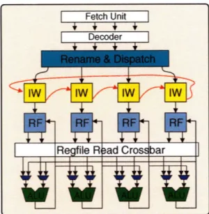
Several other schemes for dependence-based scheduling [KF96, PJS97] attempt to steer up to N depen-dent instructions from a dispatch buffer to one of N distributed instruction windows. The motivation is to localize wakeup processing in each window and to avoid considering dependent instructions in the select process. However, the simple FIFO-based approach presented by Palacharla et al. [PJS97] still requires that
N. dependent instructions can be steered into the tail of a FIFO at dispatch time as shown in Figure 2-11.
This results in an N x N2 interconnect crossbar to allow any of the N dispatched instructions to connect to any of the N dispatch ports on any of the N FIFOs.
2.4.6 Other Related
To simplify the select-logic, some designers use separate groups of reservation stations [Tom67] for each functional units, such as in various IBM Power architecture implementations [TDF+01]. Nevertheless,
Dispatch
I I I I
Issue
Figure 2-11: Distributed FIFO structured issue window.
Figure 2-12 shows that the result tag broadcast still needs to be sent to all the issue queues, and the dis-patch network can become large if multiple instructions can be sent to one functional unit. Ponomarev et al. [PKE+03] decreases the energy consumption of issue queue by using circuit techniques but doesn't improve the latency.
Dispatch
1 1 1 1~
Wakeup
1i-i-6-Figure 2-12: Reservation station style issue window design.
2.5 Motivation for Banked Microarchitectures
As reviewed above, several proposals have attempted to reduce the cost of one component of a superscalar architecture (e.g., just the register file or just the issue window), but often with a large increase in overall pipeline control complexity or possibly needing compensating enhancements to other portions of the ma-chine (e.g., extending the bypass network to forward values queued in write buffers ahead of limited regfile write ports). Also, many schemes optimize only latency not area or power. This motivates the work in this thesis to develop a new out-of-order superscalar microarchitecture that simplifies all the major components in the instruction flow to increase area and power efficiency without excessive pipeline control complexity.
Clustering is a common approach to resolve the scalability problem of highly centralized superscalar + ii !(¸¸i4 ¸ ! i + +l
N X N2 Crossbar
FIFO
FIFO
FIFO
FIFO
Dispatch Crossbar
Figure 2-13: A multibanked architecture design.
;structures. Although decentralized microarchitectures reduce intra-cluster latency and have the potential to scale to larger issue widths, they require complex logic to map instructions to clusters and to manage communication of values between clusters. Clustered architectures also tend to be less area efficient as they typically have low utilization of the aggregate resources [RF98]. I believe these are the reasons that few clustered processors have been implemented commercially. Alternatively, banked microarchitectures have attract many researchers' attention because of their ability to reduce area, power, and access time. Banking is more effective than clustering for moderate scale machines. In a cluster architecture, each cluster contains one slice of each major microarchitectural component (issue window, register file, functional units, and bypass network) placed close to each other. Multiple clusters are then connected with some lower-bandwidth inter-cluster communication mechanism. In a banked architecture, the slices within each component are placed next to each other, then components are interconnected in much the same way as in a monolithic design. This can be seen in Figure 2-13, where the regfile is a monolithic block divided into banks, where any column's ALU can read data from any bank. Another example is that all ALUs of a design with banked structures would be co-located in the same datapath to give very fast and low energy bypassing.
The contribution of this thesis is to improve previous work on banked regfile with a simpler and faster control scheme, and to extend banking to other parts of processor designs to reduced complexity of medium ;sized cores.
Chapter 3
Methodology
Microarchitecture designs are compared on the basis of their performance, power, area, and design com-plexity. The potential trade-off of these characteristics can be analyzed by careful study and comparison of circuits for each component individually. However, the impact of microarchitecture on overall processor performance is difficult to determine analytically due to the complex interactions between pipeline stages. In this chapter, I describe the common simulation methodology used to evaluate design alternatives. I also discuss the choice of workload and system parameters. Section 3.1 describes the general simulation frame-work, the simulation flow, and the functional blocks. Section 3.2 presents the benchmark suite and the sampling method. The machine configurations of idealized baseline processors are presented in Section 3.3. Section 3.4 summarizes the performance evaluation methodology.
3.1
Simulation framework
To characterize the behavior of banked microarchitectures, we extensively modified an existing superscalar processor simulator, SMTSIM [Tu196], to include detailed models of various banked microarchitectures and pipeline control schemes. These modifications included changes to the Rename, Dispatch, Select, Issue, Regfile, and Bypass stages of the processor pipeline.
SMTSIM [Tu196] is an instruction-level simulator that provides a cycle-accurate model of a pipelined
out-of-order superscalar processor with simultaneous multithreading. SMTSIM is written in the C program-ming language and executes the Alpha instruction set. Modifications are made to SMTSIM to represent the idealized baseline machine, which uses the same general structure as the MIPS RO1K [Yea96] and Alpha
Figure 3-1: Simulation framework.
21264 [PKE+03] processors, with a unified physical register file containing both speculative and commit-ted states. Figure 3-1 illustrates the simulation framework. Instructions are fetched, decoded, renamed, dispatched, and committed in program order while being dynamically scheduled for execution.
3.1.1 Front-End Pipeline Stages
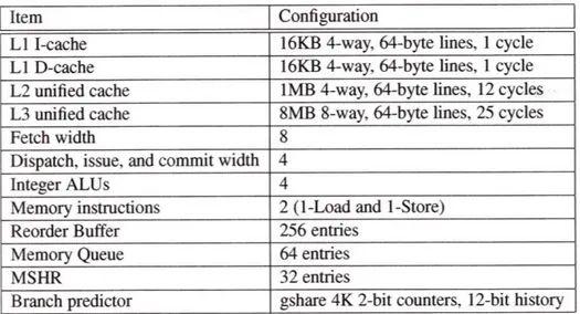
Instructions are fetched and decoded in program order. In the fetch pipeline stage, a simple global branch predictor, gshare, is used to speculatively fetch instructions. If a mispredicted branch instruction is detected during the execution stage, the processor flushes the pipeline, and restarts fetch along the correct path. The simulated results show that around 90% of branches are predicted correctly with a gshare predictor of 4K entries, 2-bit counters, 12-bit global history, and a 256-entry Branch Target Buffer (BTB). The processor uses the address of the first instruction in the fetch block to check if there is a cache miss. The fetch is stalled for a number of cycles according to the miss type. The processor resumes fetching one cycle after the cause of the stall has been resolved. During decode, each instruction attempts to allocate resources including: an entry in the reorder buffer to support in-order commit; a free physical register to hold the instruction's result value, if any; an entry in the issue window; and an entry in the memory queue, if this
is a memory instruction. A register freelist is maintained in a Last-In-First-Out (LIFO) fashion to keep track of available physical registers. If any required resource is not available, decode stalls. Otherwise, the ,architectural register operands of the instruction are renamed to point to physical registers, and the source operands are checked to see if they are already available or if the instruction must wait for the operands in the issue window. The instruction is then dispatched to the issue window, with a tag for each source operand holding its physical register number and readiness state.
3.1.2 Dynamic Instruction Scheduling and Execution
Our out-of-order superscalar machine issues instructions dynamically, potentially out of program order, depending on the presence of hazards. As earlier instructions execute, they broadcast their result tag across the issue window to wake up instructions with matching source tags. An instruction becomes a candidate for execution when all of its source operands are ready. A select circuit picks some subset of the ready instructions for execution on the available functional units. Priority is given to older instructions. Once the instructions have been selected for issue, they read operands from the physical register file and/or the bypass network and proceed to execute on the functional units. When the instructions complete execution, they write values to the physical register file and write exception status to the reorder buffer entry. When the machine knows an instruction will be executed successfully, its issue window entry can be freed.
3.1.3 Commit Stage
To preserve precise architectural state for exception handling and the illusion of sequential program execu-tion, instructions are committed from the reorder buffer (ROB) in program order. If the next instruction to commit recorded an exception in the ROB, the machine pipeline is flushed and execution continues at the exception handler. As instructions commit, they free any remaining machine resources (physical register, reorder buffer entry, memory queue entry) for use by new instructions entering decode.
3.1.4 Memory Instruction Modeling
Memory instructions require several additional steps in execution. During decode, an entry is allocated in the memory queue in program order. Memory instructions are split into address calculation and data movement sub-instructions. Store address and store data sub-instructions issue independently from the window, writing
to the memory queue on completion. Store instructions only update the cache when they commit, using address and data values from the memory queue. Load instructions are handled as a single load address calculation in the issue window. On issue, load instructions calculate the effective address then check for address dependencies on earlier store instructions buffered in the memory queue. Depending on the memory speculation policy, the load instruction will attempt to proceed using speculative data obtained either from the cache or from earlier store instructions in the memory queue (the load instruction may later require re-execution if an address is mispredicted or a violation of memory consistency is detected). For simplicity, the simulator used in this study has a perfect memory dependency predictor (i.e. load instructions are only issued after all the store instructions that it depends on are completed). Schemes such as Store-Sets [CE98] can approximate this perfect memory dependency predictor. If the load cannot proceed due to an unresolvable address or data dependency, it waits in the memory queue to reissue when the dependency is resolved. Load instructions reissuing from the memory queue are given priority for data access over newly issued loads entering the memory queue.
The scheduler always predict that load instructions will be L1 cache hits. If the load happens to be a miss, the instructions that follow are flushed out of the execution pipeline for rescheduling and a one-cycle penalty is added to recover the pipeline. To keep track of outstanding misses, the simulator models Miss. Status Handling Registers (MSHRs) [Kro81].
3.1.5 Additional Modifications
Several additional modifications are made to the original simulator to keep track of a unified physical reg-ister file organized into banks. First, a regreg-ister renaming table that maps architectural regreg-isters to physical registers is added to monitor the regfile access from each instruction. To keep track of available registers and to study the performance effect of different register renaming policies on the banked regfile, a variety of reg-ister freelists are created. Extra arbitration logic is added to each regfile bank to prevent over-subscription of read and write ports when a lesser-ported storage cell is used. Since load misses are timing critical, a write-port reservation queue is also added to give them priority over other instructions. To evaluate the per-formance impact of banking other parts of processor design, such as organizing an N-way superscalar into N columns, changes are made to the register renaming policy, dispatch logic, wakeup-select loop, and issue logic.