Atomic Engineering on 2D Materials using Electron Irradiation and
Chemical Protection
By
Cong Su
B.S., Applied Physics (2013), Yuanpei College, Peking University SUBMITTED TO THE
DEPARTMENT OF NUCLEAR SCIENCE AND ENGINEERING
IN PARTIAL FULFILLMENT OF THE REQUIREMENTS FOR THE DEGREE OF DOCTOR OF PHILOSOPHY IN NUCLEAR SCIENCE AND ENGINEERING
AT THE
MASSACHUSETTS INSTITUTE OF TECHNOLOGY February, 2020
© 2020 Massachusetts Institute of Technology All rights reserved.
Signature of Author:
Cong Su Department of Nuclear Science and Engineering
September 30, 2019 Certified by:
Ju Li Battelle Energy Alliance Professor of Nuclear Science and Engineering and Professor of Materials Science and Engineering Thesis Advisor Certified by:
Jing Kong Professor of Electrical Engineering and Computer Science Thesis Advisor Certified by:
Paola Cappellaro Esther and Harold E. Edgerton Associate Professor of Nuclear Science and Engineering Thesis Reader Certified by:
Juan-Carlos Idrobo Staff Scientist at Oak Ridge National Laboratory and Adjunct Professor of Materials Science and Engineering in Vanderbilt University Thesis Committee Member Accepted by:
Ju Li Battelle Energy Alliance Professor of Nuclear Science and Engineering and Professor of Materials Science and Engineering Chair, Department Committee on Graduate Students
Atomic Engineering on 2D Materials using Electron Irradiation and
Chemical Protection
by
Cong Su
Submitted to the Department of Nuclear Science and Engineering on Oct. 3, 2019, in partial fulfillment of the requirements for the degree of
Doctor of Philosophy
Abstract
Controlling the exact atomic structure is an ultimate form of engineering. Atomic manipulation and atom-by-atom assembly can create functional structures that are hard to synthesize
chemically. Defects with one- or few-atom-scale pertain intriguing properties that can be applicable to fields like Quantum Engineering (e.g. nitrogen vacancy center, single photon emitter, etc.), or Single-Atom Catalysis. Historically, scanning tunneling microscopy (STM) has demonstrated good stepwise control of single atoms, leading to physicochemical insights and technological advances. However, their scalability and throughput are severely limited by the mechanical probe movements, and its applicability is constrained by the low-temperature environment (usually lower than 77K) needed for stabilize the structure. Therefore, a method of controlling atoms at room-temperature without mechanical movement is essential for a broader interest and unleashing the constraints. The advancement of aberration corrector makes it possible to focus high-energy (usually ranging from 30 keV to 300 keV) electron beams to a single-atom scale inside scanning transmission electron microscope (STEM). Despite being a versatile tool for characterizing the precise atomic structures of materials, STEM has also demonstrated the capability of controlling atoms on two-dimensional (2D) materials, like a substitutional dopant in graphene or molybdenum disulfides (MoS2). This turns the irradiation
damage of electron beam (which is not what we want) to a powerful tool with a positive value (what we want). While controlling atoms using STEM is promising, it is still haunted by the fact that most of the dynamic processes are random.
The core of this thesis, a theoretical framework called Primary Knock-on Space (PKS), will be introduced for optimizing the control process by biasing the possibilities of different atomic dynamics. This framework predicts how various external factors tunable in experiment, such as temperature, electron beam incident angle, electron beam voltage, and dopant species, can influence the atom dynamics. It is proved to be useful in guiding the control process towards a more deterministic route. Following the introduction of the framework, several proof-of-concept experiments are demonstrated for validating the PKS framework. The future of Atomic
Engineering will also be envisioned at the end. An additional corrosion inhibition of 2D materials will also be discussed, which is found to be critical during the materials transfer process.
Thesis Advisor: Ju Li
Title: Battelle Energy Alliance Professor of Nuclear Science and Engineering and Professor of Materials Science and Engineering
Thesis Advisor: Jing Kong
Title: Professor of Electrical Engineering and Computer Science Thesis Reader: Paola Cappellaro
Title: Esther and Harold E. Edgerton Associate Professor of Nuclear Science and Engineering Thesis Committee Member: Juan-Carlos Idrobo
Title: Staff Scientist at Oak Ridge National Laboratory and Adjunct Professor of Materials Science and Engineering in Vanderbilt University
Acknowledgments
Six years are a long time, and it is hard to believe that I have already been in MIT for more than the period of my middle school and high school combined. Six years are also short, as I can still clearly remember the very first day when I came to MIT, and recall my thrill when I stepped into a land of wonder. Ph.D. program is hard, in the sense that there are a lot more uncertainties than I expected. It is also easy, thanks to the support of all the people who helped me with their extraordinary expertise while I was struggling on my way. It is these fantastic individuals I met that really helped form the shape of this thesis that you are reading here.
After my first year enjoying my life with a bunch of courses that I deemed to be not that hard, I was assigned by Prof. Ju Li with a clear simple task: “try moving atoms”. For one thing, he told me that atomic-level fabrication is clearly a trend after the hype of nano engineering, where human instinct is to pursue a technique with increasingly higher precision. For the other, I was told that I am obliged to contribute to nuclear engineering as I’m officially affiliated under NSE, so that the project, “elastic strain engineering” I was initially assigned, sounds like a peripheral project that I can bearly contribute a substantial amount of knowledge to nuclear science. I was convinced. The very first few months was a real struggle: I had zero knowledge about how to move atoms, nor did I know any technique I can use for moving atoms. The only thing I remembered at that time was a picture with “IBM” logo appeared on my high school textbook.
One day, there was one paper published on Physical Review Letters that caught my attention. It was a newly published paper talking about the a dopant atom exchanging its site with the neighbor carbon atom when they are scanned by high energy electron beam. That was such a eureka moment and I realized that it is exactly what I’m looking for. The technique seems to be able to control atoms, and the electron irradiation effect had been taught in the course. There were two problems I was facing though: 1. I don’t know where I can get the doped graphene sample to start with; 2. To complete this experiment, I need to use high-end electron
microscope equipped with aberration corrector. Harvard has one, but it was a TEM which is not specialized to focus electron into a small probe. I didn’t know where I can find the proper machine for looking at the atoms, let alone moving them.
To solve my first problem, I found Prof. Jing Kong, who later became my co-advisor in Ph.D. thesis, and one of my most important mentors in my career path. Jing has a very soft voice and was willing to give me advice on how I can get my samples. But she warned me the risk of this project, and kindly suggested me focus on the qualification exam before anything else should be discussed further. As a final remark, Jing asked me to meet with Prof. Mildred Dresselhaus for some advice. Mille, also been known as the “Queen of Carbon”, was reluctant to encourage me to keep on this project after patiently listening to my ten-minute soliciting and bragging about this project. But luckily, she agreed to become my thesis committee member and told me to “come and find her if it doesn’t work out well”. She also suggested me think about three things: electron excitation states, temperature, and beam energy, which all turned out to be critical factors in Atomic Engineering. It was not until the very final moment when I got recommendation letter from Ju for a postdoc position, that I knew all my advisors actually thought this topic was a risky choice.
It was indeed a risky choice if I was not struck by this last piece of luck. Nion, the electron microscope company, invited me to visit their campus after I expressed my willingness to have a summer internship there. During my visit, I met Wu Zhou, who authored multiple papers on single atom characterization and later became a professor back in China. He recommended me contact Prof. Juan-Carlos Idrobo, a staff scientist in Oak Ridge National Lab (ORNL) and a joint professor in University of Vanderbilt. To meet Juan in person, I attended the Microscopy and Microanalysis conference held in Columbus, Ohio. We discussed on the topic, I promised to submit a proposal to ORNL, and later, my proposal got accepted. The second problem was finally solved, and at the end of 2016, I embarked on this project.
The rest of my three years has been well depicted by this thesis, so no spoiler here.
my way to this thesis. Ju Li and Jing Kong, being my two advisors, gave me endless support and endorsement after I determined to commit to this project. I would also want to thank Juan-Carlos Idrobo for the time we spent together optimizing the microscope and for sharing his insights on the problem we encountered. Also, I want to thank Ondrej Krivanek and Niklas Dellby from Nion for giving me the opportunity to experience working in a boutique company that produce the world-class microscopes, to all my important collaborators, Toma Susi, Jani Kotakoski, Mingdong Dong, Zegao Wang, Zongyou Yin, Qing-Bo Yan for their contribution to this project. A special thanks to all the members from two groups, especially Cosmi Y. Lin, Haozhe Wang, Zhi Zhu, Kangpyo So, Yunfan Guo for the collaborations on the projects that yield a lot of fun.
Last but certainly not the least, I’m truly grateful to my parents who supported me along my way, and there no way I can express enough gratitude to my wife Zhuoxuan Li and my daughter Olivia for their steadfast encouragement and endless love in my hardest time.
Cong Su Barker Library of MIT
Contents
1 The Renaissance of Atomic Engineering 17
1.1 Definition of atomic engineering . . . 17
1.2 A history of single-atom manipulation . . . 18
1.3 An introduction to aberration corrected STEM . . . 20
1.4 Radiation damage as a good thing . . . 21
1.5 Uncertainty in control process . . . 22
1.6 Protecting 2D materials with a monolayer . . . 22
1.7 The structure of this thesis . . . 23
2 Single atom control using electron irradiation 25 2.1 Motivations of controlling single atoms from an application point-of-view 25 2.2 Electron-atom interaction . . . 28
2.2.1 A simple two-body collision . . . 28
2.2.2 Electron trajectory - orbital equation . . . 31
2.3 Length and time scales . . . 35
2.4 Dynamics of dopant atoms . . . 38
2.5 Primary Knock-on Space . . . 45
2.5.1 A detailed mathematical derivation of PKS . . . 46
2.5.2 Doppler amplification effect . . . 51
2.5.3 Manipulation decision tree . . . 56
2.6 Discussion on Space Charge . . . 60
2.7 The Influence of Excited States on Outcome Functions . . . 62
3 Corrosion inhibition of 2D materials with single-layer molecules 67
3.1 Motivations of corrosion inhibition . . . 67
3.2 One-pot method for hexylamine deposition . . . 68
3.3 Passivation Efficacy for Photodetectors . . . 76
3.4 Broad Applicability of 𝑛-hexylamine Coating Method . . . 77
3.5 Reversibility of 𝑛-hexylamine Coating . . . 79
3.6 Final Thoughts . . . 86
List of Figures
2-1 Transferable energy from an electron to a carbon atom moving in the direction of the electron beam. The red and blue shaded areas mark the direct exchange and knock-out zones for a C neighbor to P. In-set: Schematic illustration of head-on collision between electron and C atom, with annotations matching the derivation above. . . 31 2-2 Scattering angle as a function of impact parameter. Inset: a blow-up
of the curve close to impact parameter, 𝑏=0. . . 34 2-3 The cross sections of different electron atom interaction processes. The
atomic nucleus is represented by a purple circle in the middle, which is on the order of 10−15 m. . . . 36
2-4 The time scale of five processes in the occurance order: elastic collision, inelastic collision, excited state relaxation, lattice vibration relaxation, and electron interval time in STEM. “Step 1” indicates the “electron →PKA” process, and “Step 2” indicates the “PKA → lattice” process. 37 2-5 Illustration of competing experimental P dopant dynamics in graphene
and its control. . . 39 2-6 STEM MAADF images (raw data) of the single-layer and double-layer
graphene area where P dopant atoms are spotted. . . 41 2-7 Mechanisms of P dopant dynamics in graphene calculated with
ab-initio molecular dynamics. . . 42 2-8 Comparison of dynamics of different impurity elements. . . 44 2-9 Primary Knock-on Space (PKS): a scheme for evaluating relative
2-10 The selective dynamics by tilting electron beam. . . 50 2-11 Derivation of final velocity of PKA when it is not static before
inter-action, by transitioning between lab frame and center of mass frame. 52 2-12 The modified ovoid when PKA is not static before interaction. . . 53 2-13 A decision tree for engineering atom configurations in doped graphene. 56 2-14 The selective dynamics from 55-77 structure back to honeycomb when
beam tilted. . . 58 2-15 Elapsed time as a function of ˜𝑟 = 𝑟/𝑟0 when 𝑟0 = 1 Å. Left panel:
when ˜𝑟 is close to 1; right panel: when ˜𝑟 ≫ 1, which becomes a linear function. . . 62 3-1 Coating 𝑛-hexylamine on BP flakes and aging test with Raman
spec-troscopy. . . 69 3-2 The mechanism of 𝑛-hexylamine coating on BP. . . 72 3-3 Seven different configurations for direct adsorption of n-hexylamine on
BP. For each configuration, the front view and side view are shown, and the adsorption energy is marked under each configuration. The largest adsorption energy is only 0.33 eV. . . 73 3-4 (A, C) For direct adsorption of 𝑛-hexylamine on BP, two special initial
configurations have been tested, in which 𝑛-hexylamines are chemically bonded with BP. (B, D) After optimization, 𝑛-hexylamines in these two configurations have been repelled by BP, indicating that direct chemical bonding between 𝑛-hexylamines and BP is not possible. . . 74 3-5 Four different configurations for adsorption of 𝑛-hexylamine on
oxi-dized BP. The largest adsorption energy is 0.419 eV, indicating that oxidization of BP can enhance adsorption between BP and 𝑛-hexylamine. 74 3-6 The binding energy of Various configurations when water molecule is
involved. . . 75 3-7 The definition of coverage on BP. . . 75
3-8 The structures of HA-BP used for calculating H2O and O2 molecules
penetrating through the 𝑛-hexylamine coating. For each coverage and penetrating molecule type, three different locations are shown (far, middle, and close to the BP surface respectively), and each location is shown in two perspectives which are top view and side view. The distance 𝑑 is defined in the first two figures of H2O and O2 in 25%
coverage. . . 81 3-9 Photodetectors and etching test. . . 82 3-10 Removability of 𝑛-hexylamine coating on BP by organic acid. . . 83 3-11 AFM data of the reversible process of 𝑛-hexylamine coating on BP and
WSe2. . . 84
4-1 The flow chart of one single step in Atomic Engineering with automatic image recognition and control feedback. The core of control strategy is determined by PKS theory developed in Chapter 3. Image credit: Nion. . . 88 4-2 The stacked structure of 2D materials. With the capability of
pen-etrating through thin layers with little degradation of electron beam wave front, focused electron beams can be used for controlling atoms on different layers and harnessing the z-dimension. . . 89
List of Tables
2.1 Lifetime of inelastic excitations in some common 2D materials. . . 63 3.1 Coating parameters for amine and hexane molecules on 2D materials,
for example BP in this work. . . 76 3.2 Coating parameters optimization of n-hexylamine on BP based on the
protection testing results by taking optical microscope images before and after etching/oxidation of BP flakes. The etching method with H2O2 (30% wt. in H2O) etchant/oxidant follows: dip BP into H2O2
for 20 sec, remove BP from H2O2, and leave dipped BP for 2 mins in
air. Scale bars are 20 𝜇m. . . 78 3.3 Comparison between existing protection techniques. Factors such as
coating layer thickness, resistive property, and techniques used are com-pared. . . 85
Chapter 1
The Renaissance of Atomic
Engineering
1.1
Definition of atomic engineering
To begin with, we will discuss about the concept of “Atomic Engineering”, and its spe-cific meaning related to this thesis. This terminology has been first used by Theodore von Kármán from California Institute of Techonology in 1946, where he wrote [1]:
“And now it seems we are at the threshold of the new atomic age. I do not know whether or not this is true, but certainly, we shall have ‘atomic engineering’ in the fields of power and transportation. Are we prepared for the problems involved?”
The usage of “atomic” as a modifier in front of a noun is usually interchangeably used with “nuclear”, where cases of “atomic bomb” or “atomic power” follow. However, the usage of “nuclear bomb” or “nuclear power” are more proper here, as in these cases, it is only nucleus being a part of atom that plays the critical role, while the electrons outside of nucleus plays a minimum role. When “atomic” is used as an adjective, it should refer to an entity or event involving the whole atom. “Engineering”, on the other hand, is defined in Wikipedia as “the use of scientific principles to design and build machines, structures, and other items”. The human interactions
with the surrounding nature can be categorized by the direction of information flow as: learning from the environment (human input), and modifying the environment (human output). It happens likewise as how we distinguish the knowledge body into “science” and “engineering”. “Science” falls into the first category, where human gets input from the outside world and process this set of information with induction and conduction. “Engineering” belongs to the latter category, where human utilize the knowledge pool established from “scientific learning” and make an output back to the nature to modify something. Therefore, “Atomic Engineering” might be a superset of nuclear engineering, where it can be defined as “exploiting the atomic characters of matter for engineering applications”. From this definition, atomic engineering refers to any engineering purpose that harnesses the different degrees of freedom of an atom, such as its spatial location and the electronic state. In our thesis, we focus only on the atom location, as the definition is further narrowed down to “controlling the atomic configuration of matter for engineering applications”. This definition has confined our event to be mainly within the realm of “controlling the position of atoms” or “atom-by-atom fabrication” for realizing an application that might be only reachable by controlling the structure down to atomic scale.
1.2
A history of single-atom manipulation
To zoom out our scope a bit, ultra-fine machinery in engineering has always been dubbed as a critical technique in high-end manufacturing. Traditionally, the ma-terials are created using a “top-down” method, where the synthesis process itself is the focus of the materials fabrication and the target material is created as-a-whole. Macroscopic parameters such as temperature, pressure, chemical precursors, gas envi-ronment, electric voltage, magnetic field etc., are tuned for reaching the final product that is also desired and expected to manifest a homogeneous property in a long range scale. By switching these external parameters, it is possible to modulate the frontier boundary of the material during growth process (the 0D frontier end of a 1D material, the 1D frontier edge of a 2D material, or the 2D frontier surface of a 3D material), but
it is impossible to control the features of a materials that is two-dimension lower (like controlling a 0D defect feature in 2D materials). A more advanced structural control technique renders more capability in quality control and more flexibility in materials design process. The ability to create structures with special units in a short-range scale (in our case, as short as the length scale of an atom) could integrate various functions condensed in a small footprint, with the feature density of 𝑛2compared with
𝑛 as in tuning the macroscopic parameters. This “bottom-up” view of creating mate-rial structures is reminiscent of transistors and integrated circuit devices flourished in the 20th century, where transistors with different functional units are integrated into a single chip board, following a trend predicted by the renowned Moore’s Law [2]. With unit transistors reaching the size of several atomic scale, the developing trend of the transistor industry no longer follows Moore’s Law, where traditional fabrication method fails as expected and quantum effect turns to dominate at this length scale [3]. Investigating the atomic scale properties (where localization effect dominates and the periodic boundary condition in a crystal-viewpoint no longer holds) and looking for a path to control single atoms (where each atom needs to form a certain structure as designed) are essential and urgently needed. Thus, controlling single atom can be regarded as an ultimate form of material engineering where the smallest unit that still represent the property of the substance act as a building block. By scaling up the control steps, a group of engineered atoms collectively contributing to a pre-designed function. With one order of magnitude lower in scale than nano-engineering (10−9
m), atomic engineering (10−10 m) is deemed to be much more difficult. Almost two
decades ago, scanning tunneling microscope (STM) demonstrated its first success in manipulating adsorbed atoms on the metal surface [4, 5]. It is followed by atomic force microscope (AFM) which also showed its capability in moving vacancies on the surface [6]. Due to the complexity of designing the atomic-scale AFM when compared with STM, it is not until about 19 years after its invention has the AFM successfully manipulated the first atom. STM and AFM belong to a superset category called scanning probe microscope (SPM). The problems of controlling atoms using SPMs are evident:
1. Low temperature: The samples are usually kept under very low temperature, which usually needs liquid helium to stabilize.
2. Slow: The mechanical movement of metal probe is very slow.
3. Surface limitation: Only the atoms on the surface of bulk material can be modified.
How to address these problems is critical in up-scaling Atomic Engineering which is the main point of this thesis.
1.3
An introduction to aberration corrected STEM
Other than SPMs, another imaging technique that has atomic resolving capability is scanning transmission electron microscope (STEM) has a much longer history than the above SPMs, but it was not until the success invention of aberration-corrector that the true atomic resolution images can be routinely obtained by normal users. “Aberration” of an optical component (or electron optical component in our context) is a deviation from the ideal light path that is intended to be created, mainly caused by intrinsic physical law or the defective manufacturing of an optical component. For example, in a traditional electron microscope, the electrons are focused by the round electromagnetic lens which creates an electromagnetic field. In 1936, Scherzer proved that no matter how these round lenses are modified, they all suffer from a 3rd-order spherical and first-order chromatic aberration [7]. The consequence of having such an aberration is that the electron probe cannot be focused onto the same length scale as a single atom. Later, he proposed that by using multipole magnetic lenses, these aberrations can be compensated, which leads to the invention of modern corrector. With the aberration fixed by the corrector, the width of electron probe is improved to be 1 Å, on the order of the size of an atom. The capability of focusing high energy electrons on an atom directly leads to the advent of atomic-resolved imaging and single-atom spectroscopy [8,9]. This also creates opportunity to selectively focus electron beams to modify a single atom.1.4
Radiation damage as a good thing
Due to the nature of electron beam, it is only the projection image along the z-direction of the materials that can be created (expect for confocal techniques which still has a z-direction resolution on the order of 10 nm). With the layer distance to be around half a nanometer, no atomic-level information can be extracted layer-by-layer inside STEM/TEM; therefore, it is only an “atomic column” that can be put under electron beam and no atom manipulation can be done. The birth of two-dimensional (2D) materials have changed this situation. With only one-atomic layer, WYSIWYG (“what you see is what you get”) is truly realized in STEM. The atom species can be distinguished by the contrast of atoms (Z-contrast imaging [10]) or the single-atom electron energy loss spectroscopy (EELS) [11].
STEM has been designed as a tool for “seeing” atoms in the first place. The radiation damage from high energy electron beam on materials has always been a side effect that is to be avoided rather than embraced in STEM. It was not until decades later it was invented, the true demonstration of successful single-atom manipulation was done by Susi etc. [12] and Dyck etc. [13]. It is at this time point that the radiation damage is truly turned from something bad to good.
When comparing these atom-control techniques, they should be categorized into two different groups, according to the energy barrier involved in moving the atoms: (1) STM and AFM control the surface adsorbed atoms which lightly adhere to the surface of host matrix through van der Waals interaction, and the metal uses what is called “metallic adhesion” to push or pull the atom [14]. Like 3D printing, STM and AFM can in principle pile up a structure atom-by-atom thanks to the nature of surface modification. The built-up atomic pile is the functional structure with rather small coupling to the substrate. (2) On the contrary, STEM modifies the crystal structure and covalent chemical bond. The atom manipulation involves a bond breaking on the energy level of 10 eV and a reformation of chemical bonds afterwards. This modification can only be realized by high energy electrons (30-200 keV) which is able to transfer enough energy to atoms (∼10 eV for low Z elements) for completing this
task. Since the atom is covalent-bonded to the materials structure, local density of states (DOS) of the host matrix will be altered through the modification of atom position, which may be coupled to other properties of the host matrix.
1.5
Uncertainty in control process
In this thesis, we use STEM to both drive and identify the atomic motion of individual phosphorus (P) dopants in graphene, and construct a theoretical scheme for evaluating their relative probabilities with respect to electron energy and momentum direction [15]. In stark contrast to the Si dopant where the movement is relatively easy to induce, P is much harder to control. When we try to move P atom, what we found is that various dynamics process is induced instead of the dynamic we desire. These dynamic processes are categorized into four types: (A) direct exchange and (B) Stone-Wales (SW) transition, which conserve the atoms, plus (C) knockout of a carbon neighbor and (D) replacement of a dopant atom by C, which do not conserve the local composition. We choose to use 60 keV electron energy (electron velocity is 0.4462c = 1.3377×10⁸ m/s) to minimize (C)+(D) while maximizing the rates of direct
exchange and SW transition. Just like the Si case, instead of aiming the electron beam directly at the dopant itself, it has been established that dynamics can be more effectively induced when the electron beam is aimed at a carbon neighbor of the dopant [12, 16]. Our goal in this thesis is to maximize the desire probability while reducing the undesired ones.
1.6
Protecting 2D materials with a monolayer
Other than graphene and hexagonal boron nitride (hBN), almost all the other 2D materials are easy to get corroded in air [17]. One biggest problem during the materi-als transport between MIT and ORNL is that some of the samples degrade very fast, and we cannot preserve its original crystal lattice after a long flight. That motivates me to investigate further into this, where our goal is to preserve the crystal lattice
of 2D materials as intact as possible during transport, and when we arrive at the destination, the protection layer is still able to be removed.
But this is by no means an easy task. When we consider kinetic passivation of two-dimensional (2D) crystals [18–23], it should be even more essential because (a) the thickness of passivation layer 𝑑p(𝑡) on 3D materials like Si, Al, Mg etc. stays 3-5
nm over very long time 𝑡, which is insignificant fraction of the remaining unreacted material. However, one cannot say this for a thin 2D material whose total thickness is 𝑑s, which is likely comparable to 𝑑p(𝑡). In other words, we must ensure 𝑑s > 2𝑑p(𝑡)
for a free-standing sample over an extended period in order to utilize the intrinsic properties of the native material exposed to ambient environments. (b) The functional properties of 2D crystals are extremely sensitive to its thickness (i.e. 𝑑s−2𝑑p(𝑡)) down
to a single monolayer. Therefore, meticulous corrosion control down to the level of few-/single-layer is practically useful. (c) The thickness and type of passivation might also provide a natural opportunity to engineer extremely thin vertical heterostructures for information processing applications. For these reasons, fundamental study of passivating 2D crystals is important, in addition to its obvious practical significance.
1.7
The structure of this thesis
This thesis consists of two main sections. Chapter 2 is going to introduce the back-ground of elastic and inelastic atom-electron interacts, and the typical length scales and time scales of various dynamic processes. Then we will get into the dynam-ics of single atomic dopant under the irradiation of high energy electron source. A theoretical framework called Primary Knock-on Space (PKS) will be developed for optimizing the atom control process. Several caveats of electron-atom interaction is also discussed with detailed derivations. Chapter 3 deals with the corrosion problem of 2D materials, where a molecular monolayer is deposited on the protected 2D mate-rials. To start with, the coating procedure and parameters are carefully chosen, and detailed characterizations have done to investigate the structures of the thin coating. Application-wise, a photoelectric device with the coating has been demonstrated to
be effective in resist harsh environment. A density function theory (DFT) model is used to interpret the mechanism and shows the waterproof function of the surface layer. Finally, Chapter 4 serves as an envision of the possible applications of PKS in Atomic Engineering, and where Atomic Engineering might leads to. We propose an architecture where controlling atoms is done with automatic program controlled by PKS theory. We also propose at the end a 3D stacking architecture harnessing the penetration depth of high energy electrons.
Chapter 2
Single atom control using electron
irradiation
2.1
Motivations of controlling single atoms from an
application point-of-view
As nanotechnology has been developed into a well-integrated realm consists of science, engineering, and technology that manipulates matter from 1nm to 100nm, we have hit some limits that is bounded by the physical law "on the bottom". The state-of-the-art nanotechnology might push this limit down to 1 nm by integrating carbon nanotubes into transistors. That seems to be a small enough transistor size, until we realize that shrinking size by one order of magnitude in transistor may only takes about 5-10 years before. The scale level that goes beneath the nanometer-level is the atomic level, and surface atom manipulation has only been done by STM three decades ago. The limitation of surface scanning as well as the stringent operation conditions of STM also confines its application and its transition to the real world. Here, we are designing another way of manipulating the atoms from the ground-up using electron microscope.
Atomic Engineering is defined in the introduction as “controlling the atomic con-figurations of matter for engineering applications". Apart from STM, most of the
other control in sub-atomic level is fulfilled by manipulating nuclear spin, while keep-ing the atom configuration untouched, as in nuclear magnetic resonance (NMR). In NMR, the configuration of atoms are kept intact, while only the nuclear spin is con-trolled by the external field. However, the motivation to modify materials on atomic level is quite strong and self-evident. On one hand, it is human instinct that we should proactively seeking fabrication tools that renders us with more precision. On the other hand, cranking up areal density for memory is a tendency driven either by the business market or an idiosyncrasy of following the Moore’s Law [24], which rules the semiconductor world for decades and hardly failed. Assuming if Moore’s Law still works for the next several decades, we need to be able to control single atoms for storing information in 25 years.
Given the fact that Atomic Engineering might be applied in information storage, it is warranted to have a very brief introduction of storage technology history here and how Moore’s Law can fail. Information storage technology is developing rapidly thanks to the much more sophisticated manufacturing process in nano-materials and a deeper understanding in optical and magnetic physics. In 2007, Albert Fert and Peter Grunberg were awarded the Nobel Prize in Physics for the discovery of giant magne-toresistance (GMR), paving the foundation of the present hard disk drive industry. In the mid-2000s, when the magnetized recording domain becomes smaller, people started to realize that the so-called superparamagnetism is a pressing issue [25]. In large uniaxial anisotropy material, spontaneous reversal of the magnetization vector could happen when the temperature is high enough. Grain magnetization flipping is a thermal activation process governed by the Néel-Arrhenius equation giving a time constant 𝜏:
1
𝜏 = 𝑓0exp(−𝐸B/𝑘B𝑇 ) (2.1) where 𝑓0 is the attempt frequency determined by intrinsic magnetic properties and
is of the order of 109− 1012 Hz, and 𝐸
of two states of the magnetic polarization of a grain, which could be calculated as 𝐸B = 𝐾𝑢𝑉 where 𝐾𝑢 is the uniaxial constant of a material, and 𝑉 is the grain volume.
The key issue needs to resolve in a traditional hard disk drive industry are reconciling a trilemma involving grain size, media anisotropy, and the write element magnetic field [25]. Grain size and media anisotropy are two “conjugate" quantities which is hard to be improved together, which could be seen in Equation (2.1): when the grain volume shrinks down, the activation barrier becomes smaller, and the vector flipping becomes more frequent. A large write element magnetic field is required to flip the magnetic polarization, which is usually 2.4 Tesla by using CoFe head developed early in 1990s, and no more increase thereafter [25]. These three quantities together define the performance of the data recording media, and an upper ceiling is about to be hit. If we want to continue the trend of transister development, new ways to control atoms needs to be found in order for the device to work properly in room temperature.
To reiterate, controlling the exact atomic structure of materials is an ultimate form of engineering [26, 27]. Atomic manipulation and atom-by-atom assembly can create functional structures that are hard to synthesize chemically [16, 28–30], e.g. positioning atomic dopants exactly to modify the properties of carbon nanotubes and graphene [31]. Nitrogen (N) or phosphorus (P) dopants might be useful in quantum informatics due to non-zero nuclear spin [32], similar to the use of the nitrogen vacancy (NV) center.
Successful atomic engineering requires understanding of two parts:
1. how the desirable local configurational changes can be induced to increase the speed and success rate of control;
2. how to scale up basic unit-processes into feasible structural assemblies of 1-1000 atoms to produce the desired functionality.
Historically, scanning tunneling microscopy (STM) [33] have demonstrated good stepwise control of single atoms, leading to physicochemical insights and technological advances [34]. However, their scalability and throughput are severely limited by the mechanical probe movements. Scanning transmission electron microscope (STEM)
is an optical-microscope-equivalent using electron source for imaging. With the de-velopment of aberration corrector, it can focus electron beams into fine probes with a full width half maximum at around 1 Å. It has emerged as a versatile tool for characterizing the precise atomic structure of materials [8,9,35–41]. Despite its very early stage of development, STEM also shows great promise as a tool for atomic ma-nipulation: in two-dimensional (2D) graphene, Si dopants are found to be stepwise controllable [13, 41, 42] and iterating these basic steps enables long-range movement with a high throughput [43], whereas in a three-dimensional (3D) silicon crystal, the projected location of Bi dopants was also manipulated [44]. However, imprecise under-standing of the dynamics of the basic steps, which involves relativistic electron-nucleus collisions, electronic excitation and relaxation, dynamic ion trajectories, momenta de-phasing and heat conduction, add uncertainty to this technique. While the traditional theory of radiation damage provides a basis for understanding, instead of trying to minimize beam effects atomic engineering seeks to control them in order to achieve desired configurational changes. Concepts like the displacement threshold energy 𝐸𝑑,
which is in most cases approximated as scalar, turns out to be too crude to guide the design of the precise branching rates of different configurational outcomes [45,46].
2.2
Electron-atom interaction
2.2.1
A simple two-body collision
The transferrable energy from a high energy electron to a static carbon atom can be estimated using the following relation:
𝐸 = ˜ 𝐸e( ˜𝐸e+ 1.02) 496𝐴 sin 2𝜓 2 (2.2)
where ˜𝐸e is the incident electron energy in MeV, 𝐸 is the transferred energy to a
static nucleus in MeV, 𝐴 is atomic mass number (e.g. ∼12 for carbon), and 𝜓 is the scattering angle of the electron (when 𝜓 = 0 no interaction happens and 𝐸 = 0; when 𝜓 = 𝜋, back scattering happens and 𝐸 is maximum). It can thus be estimated that
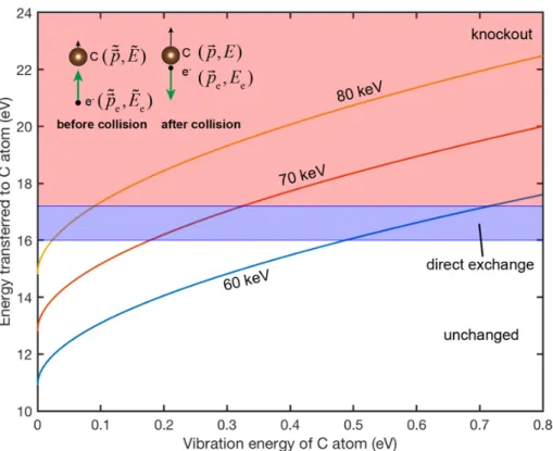
the maximum energy transferable to a C atom is 10.9 eV for a 60 keV electron, which would mean that all dynamic processes should be prohibited since the lowest energy required for inducing a lattice change in P-doped graphene is larger than 14 eV.
However, the lattice of graphene is not static. Due to thermal vibrations, the atoms of the lattice are in motion, which relaxes the momentum conservation con-dition and increases the transferable energy under the irradiation of a high energy electron beam. Even at 0K, the zero-point energy resulted from Heisenberg uncer-tainty principle would also leads to a non-static atom dynamics. The contribution from this lattice vibration will be discussed in detail in the following Doppler Ampli-fication Effect section. Here, to simplify the picture, our following derivation assumes a head-on collision between an electron and a C atom (𝜃e= 0).
Consider the conservation of momentum and energy, we have
˜
pe+ ˜p = pe− p, (2.3)
˜
𝐸e+ ˜𝐸 = 𝐸e+ 𝐸, (2.4)
where ˜pe, ˜𝐸e, pe, 𝐸edenote the momentum and energy of electron before (with ˜) and
after (without ˜) collision, with ˜p, ˜𝐸, p, 𝐸 being the counterparts for the nucleus. The momentum is related to energy relativistically for the electron (inside STEM, the electron is traveling at half of the light speed), and non-relativistically for the nucleus: |pe| = 1 𝑐 √︀ 2𝐸e𝐸0+ 𝐸e2, (2.5) |p| =√2𝑀 𝐸, (2.6)
get 1 𝑐 √︁ 2 ˜𝐸e𝐸0 + ˜𝐸e2+ √︀ 2𝑀 ˜𝐸 =√2𝑀 𝐸 −1 𝑐 √︁ 2( ˜𝐸e+ ˜𝐸 − 𝐸)𝐸0+ ( ˜𝐸e+ ˜𝐸 − 𝐸) 2 . (2.7)
Since the kinetic energy of the nucleus is much smaller than that of the electron in all stages, we can approximate ˜𝐸e+ ˜𝐸 − 𝐸 into ˜𝐸e, and get the following expression:
√
2𝑀 𝐸 =√︀2𝑀 ˜𝐸 +2 𝑐
√︁
2 ˜𝐸e𝐸0+ ˜𝐸e2. (2.8)
For a static nucleus before collision ( ˜𝐸 = 0), we have √︀ 2𝑀 𝐸stat = 2 𝑐 √︁ 2 ˜𝐸e𝐸0 + ˜𝐸e2, (2.9)
where 𝐸stat is the transferred energy from electron to a static atom. Subtracting the
above equations gives
√
𝐸 =√︀ ˜𝐸 +√︀𝐸stat. (2.10)
This relation between the final energy of PKA (𝐸) and the atom vibration energy ( ˜𝐸) can be plotted as Figure 2-1. Therefore, to activate a direct exchange process, a vibration energy of 0.5 eV is enough. Although the average kinetic energy of atoms at room temperature is much smaller (0.025 eV), their velocities follow a normal distribution with a width given by the mean-square velocity (or corresponding kinetic energy), leading to a finite population of atoms with high kinetic energies at the moment of impact.
The probability distribution of out-of-plane velocities of carbon atoms in graphene can be estimated using [47]:
𝑃 (𝑣𝑧, 𝑇 ) = 1 √︀ 2𝜋 ¯𝑣2 𝑧(𝑇 ) exp (︂ 𝑣2 𝑧 2 ¯𝑣2 𝑧(𝑇 ) )︂ (2.11) To get a sense of how rare these events are, the probabilities of vibrational energy above a certain level are: (1) 0.1 eV: 0.0122; (2) 0.2 eV: 7.2×10⁻⁴; (3) 0.3 eV: 4.8×10⁻⁵;
Figure 2-1: Transferable energy from an electron to a carbon atom moving in the direction of the electron beam. The red and blue shaded areas mark the direct exchange and knock-out zones for a C neighbor to P. Inset: Schematic illustration of head-on collision between electron and C atom, with annotations matching the derivation above.
rare, such vibrations do yield finite cross sections for events that would be otherwise forbidden.
2.2.2
Electron trajectory - orbital equation
Most of the time, electron does not hit right onto the nucleus and make back scatter-ing. Therefore, the trajectory of the electron is critical when the impact parameter of electron, 𝑏, is larger than 0. Here, we introduced a very important variable “im-pact parameter” which is defined as the perpendicular distance between the path of a projectile and the center of a potential field created by an object that the projectile is approaching. In a two body system, the total energy is conserved
𝐸 = 1 2𝜇( ˙𝑟
and the total angular momentum is conserved 𝑙 = 𝜇𝑟2𝜃 ⇒ ˙˙ 𝜃 = 𝑙
𝜇𝑟2 (2.13)
where 𝑈(𝑟) is the potential between the two bodies, and 𝜇 is the reduced mass for the two bodies. 𝑙 is the angular momentum, 𝜃 and 𝑟 are the angle and distance with respect to origin in the polar coordinate. The dot above the variables represent time derivative, 𝑑/𝑑𝑡. Getting rid of ˙𝜃 by combining the above two equations, and by approximating 𝜇 to be 𝑚 as 𝑀 ≫ 𝑚, 𝐸 = 1 2𝑚 ˙𝑟 2 + 𝑙 2 2𝑚𝑟2 + 𝑈 (𝑟) (2.14)
and solving for ˙𝑟, we have
˙𝑟 = ± √︂ 2 𝑚(𝐸 − 𝑙2 2𝑚𝑟2 − 𝑈 (𝑟)). (2.15)
For orbital equation, we are interested in 𝑑𝑟/𝑑𝜃, so by using chain rule, 𝑑𝑟 𝑑𝜃 = ˙𝑟 ˙ 𝜃 = ± √︂ 2𝑚 𝑙2 𝑟 2 √︂ 𝐸 − 𝑙 2 2𝑚𝑟2 − 𝑈 (𝑟). (2.16) therefore, 𝜃 = ∫︁ 𝑑𝜃 = ±√𝑙 2𝑚 ∫︁ 𝑑𝑟 1 𝑟2√︁𝐸 − 𝑙2 2𝑚𝑟2 − 𝑈 (𝑟) . (2.17)
Specifically, in our system, 𝑈(𝑟) = −𝑘𝑄𝑞
𝑟 , so we have 𝜃 = ±√𝑙 2𝑚 ∫︁ 𝑑𝑟 1 𝑟 √︁ 𝐸𝑟2− 𝑙2 2𝑚+ 𝑘𝑄𝑞𝑟 . (2.18) Using ∫︁ 𝑑𝑟/𝑟 √ 𝑎 + 𝑏𝑟 + 𝑐𝑟2 = 1 √ −𝑎sin −1 ( 𝑏𝑟 + 2𝑎 𝑟√𝑏2− 4𝑎𝑐) (2.19)
we get 𝜃 − 𝜃0 = ± sin−1( 𝑘𝑄𝑞𝑟 − 𝑙2/𝑚 𝑟√︀𝑘2𝑄2𝑞2+ 2𝑙2𝐸/𝑚) (2.20) which is equivalent to 𝑟 = 𝑙 2/𝑘𝑄𝑞𝑚 1 ± 𝜖 sin(𝜃 − 𝜃0) (2.21) where 𝜖 = √︃ 1 + 2𝑙 2𝐸 𝑘2𝑄2𝑞2𝑚. (2.22)
By convention, we choose "+" sign and 𝜃0 = 𝜋2,
𝑟 = 𝑙
2/𝑘𝑄𝑞𝑚
1 + 𝜖 cos 𝜃 (2.23)
By converting angular momentum 𝑙 = 𝑚𝑣𝑏 where 𝑏 is the impact parameter of electron with respect to the hitting target atom, and 𝐸 = 60 keV,
𝜖 = √︃
1 + 2𝑚𝑣
2𝑏2𝐸
𝑘2𝑄2𝑞2 . (2.24)
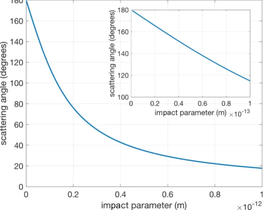
One very useful application of equation (2.23) is that we can calculate the scatter-ing angle of electron at a given impact parameter, 𝑏. The incomscatter-ing angle of electron, 𝜃0, can be calculated by setting
1 + 𝜖 cos 𝜃0 = 0. (2.25)
For example, with an impact parameter of 𝑏 = 1 × 10⁻¹³m, we have 𝜖 = 1.187,
and 𝜃0 = 147.4°. Therefore, the deflected angle is 𝛼 = 2𝜃0 − 180° = 114.8°. The
corresponding PKA scattering angle is 32.6°. A relation between the scattering angle and impact parameter is shown in Figure 2-2.
The electron trajectory is important to know since the energy transferable from an electron to an atom depends on the out-scattering angle of the electron. Dynamics can only happen when the scattering angle is large enough such that there are enough energy transferred from electron to the target atom. By using the trajectory equation,
Figure 2-2: Scattering angle as a function of impact parameter. Inset: a blow-up of the curve close to impact parameter, 𝑏=0.
we can therefore estimate the cross section of a certain dynamics very easily by knowing the minimum scattering angle required.
2.3
Length and time scales
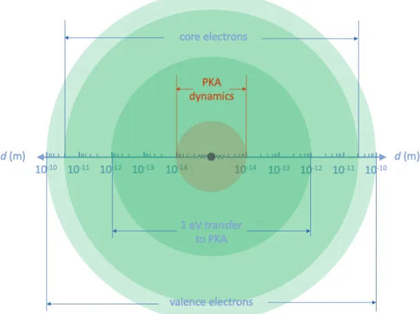
If we stand from the electron standpoint of view, and looking down on the target atoms, what we see looks like the Figure 2-3. The figure is drawn in logarithm scale for clarity, so if we convert the scale to linear scale, what one can imagine is that the area (or what is called “cross section” here) is very small for the region of where dynamics can be induced. To estimate the effective number of electrons that can induce a dynamic process, we assume 109 electrons/s (160 pA) as the current
inside STEM. The FWHM of electron probe is proved to be around 1Å so there is only 10−8 of the total electrons can be used for inducing the dynamics. That is, for
every second, there are only 10 electrons inside the microscope that fly into the cross section that can truly induce the dynamics (let’s call them “effective electrons”). In our experiment, we sometimes see that dynamics happens very fast, causing some broken rows in the scanning image.
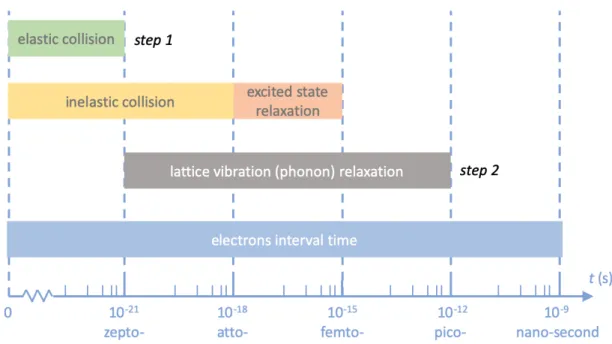
To achieve atomic configurational change, the post electron collisional energy of the primary knock-on atom (PKA; here it is carbon), 𝐸, needs to be on the order of 10 eV. This requires the penetrating electron to pass very close to the PKA nucleus (impact parameter 𝑏 < 𝑏c ∼10−14m), with corresponding collisional cross-section on
the order of barns (𝜎 ∼ 10−28 m2) (please refer to Figure 2-4). Such elastic collision
and large energy transfer occur mainly within zeptosecond timescale (𝜏c ∼ 10−22 s),
inducing a post-collisional PKA momentum labelled by a vector. With a total beam current of 𝐼 ∼ 50 pA, this amounts to about 1 relativistic electron penetrating the graphene every 3 nanoseconds (𝜏p ≡ 𝑒/𝐼 ∼ 3 ns), and one can focus the e-beam to a
spot with a full-width at half-maximum (FWHM) of 1 Å (which provides a sufficient description of the scanning beam). The collisional probability (defined as impart-ing the PKA with 𝐸 ∼ 10 eV energy, that may cause “immediate" configurational change within picoseconds) is thus only ∼ 𝜎/FWHM2 ∼ 10−8 per penetration event,
Figure 2-3: The cross sections of different electron atom interaction processes. The atomic nucleus is represented by a purple circle in the middle, which is on the order of 10−15 m.
or 𝜎/FWHM2
/𝜏p ∼ 10 per second (0.1 per second for events like direct exchange
with cross section of 0.01 barn); the rest of the penetration events cause electronic excitation and small ionic rattling, but not immediate local configurational change.
Regardless of whether a penetrating electron gets within 𝑏c or not, a penetration
event will cause electronic excitation, occurring with attosecond timescale 𝜏e ∼ 3.4
Å/ ˜𝑣e ∼ 10−18 s (3.4 Å being the graphene thickness), which however in the case of
graphene will relax collectively on the femtosecond timescale (𝜏E ∼ 10−15 s) to the
electronic ground state [48]. Thus after 𝜏e+ 𝜏E, the electronic subsystem falls back to
electronic equilibrium and one may use the Born-Oppenheimer (BO) approximation to describe the ion dynamics, that can either achieve the (A)-(D) configurational change (labelled by 𝑖=1...4) or unchanged (𝑖=0) on the BO surface, within a few
picoseconds (𝜏I∼ 10−12s). Since 𝜏I ≫ 𝜏e+𝜏E, it is justified here to apply ground-state
density functional theory (DFT) to track the main portion of the ion dynamics, to obtain the probability of success, 𝑃𝑖, of dynamics that lead to configurational outcome
𝑖. Throughout 𝑡 = 𝜏c, 𝜏E, 𝜏I, the PKA momentum history needs to be tracked, thus we
build a theoretical scheme called Primary Knock-on Space (PKS) for estimating the relative scattering cross sections of different electron-induced dynamics due to either sample or electron beam tilt, and for selectively activating the desired outcomes. We further provide experimental verification of our calculations, thus opening new avenues for atomic engineering using focused electron irradiation.
Figure 2-4: The time scale of five processes in the occurance order: elastic collision, inelastic collision, excited state relaxation, lattice vibration relaxation, and electron interval time in STEM. “Step 1” indicates the “electron → PKA” process, and “Step 2” indicates the “PKA → lattice” process.
We find that the P dopant in graphene can serve as a good example for covering many categories of electron-induced dynamics. With highly collimated and focused (e-beam FWHM 1 Å) electron irradiation on a carbon atom neighboring the phosphorus dopant, we occasionally create a single energetic PKA, with rate ∼ 𝑑𝜎/FWHM2
/𝜏p,
where 𝑑𝜎 is the differential cross-section corresponding to a particular post-collisional PKA differential momenta volume. To clarify, the term PKA exclusively refers here to
the energetic carbon neighbor of the phosphorus dopant, so “PKA" and “C neighbor colliding with an electron of the beam" are equivalent throughout this paper. This energetic carbon atom then drives a short burst of atomic motions nearby within 𝜏I∼
picoseconds.
2.4
Dynamics of dopant atoms
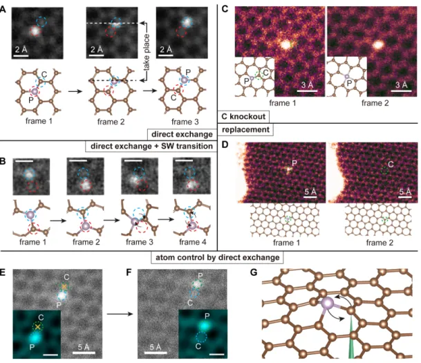
In Figure 2-5, four types of dynamics are shown, categorized into two groups: atom-conserving dynamics (which is desirable) and atom-non-atom-conserving dynamics (which is often not desirable). Atom-conserving dynamics include (A) direct exchange between P and C [Figure 2-5(A), earlier dubbed “bond inversion” in the context of Si [12]], and (B) SW transition [Figure 2-5(B)], i.e. 90° rotation of a P-C bond [46]. Atom-non-conserving dynamics include (C) knockout [Figure 2-5(C)] where the PKA is knocked out by the electron beam (P turns from three-coordinated to four-coordinated, after which we found it is no longer possible to further manipulate the configuration with 60 keV e-beam), and (D) replacement [Figure 2-5(D)], where a diffusing carbon adatom that happens to be nearby receives energy from a penetrating electron and replaces the dopant. Such wandering C adatoms are always present on graphene surfaces [12,49], but they diffuse too quickly to be imaged. In the above experiments, we scanned the beam over a square area covering the dopant atom so that the configurational changes could also be captured in frames (often as a broken “transit” frame, where part of the scanned image is discontinuous with the rest of the image that is scanned later).
In Figure 2-5(A), three consecutive frames of direct exchange including a transition frame are presented. As a result, the P dopant atom exchanges site with the PKA while the e-beam is scanning from left to right across the PKA (white dashed line; note that at each pixel, most of the electron dose is distributed within an Å-sized area surrounding it according to the beam intensity profile). In Figure 2-5(B), a SW transition is preceded by a direct exchange. After the direct exchange (frame 1 to 2), the P-C bond is rotated by 90° (frame 2 to 3), and the hexagonal lattice is locally
Figure 2-5: Illustration of competing experimental P dopant dynamics in graphene and its control.
transformed into two pairs of 5- and 7-membered rings (55-77 structure hereafter). The 55-77 structure is only stable for less than 0.2 second before reverting back to hexagons (frame 3 to 4) due to the subsequent electron irradiation. In Figure 2-5(C), a three-fold coordinated P (frame 1) turns into four-fold coordinated (frame 2) when the PKA is knocked out by the electron beam. Once this happens, we find the P can no longer be manipulated. In Figure 2-5(D), P is replaced by C, which is the most commonly observed outcome of P impurities-in stark contrast to Si, which are almost never removed or replaced. It should be noted that we never observed a phosphorous being simply knocked out leaving a vacancy behind, consistent with the prediction that its knockout cross section being several orders of magnitude smaller than that of the lighter C atoms.
As a basic step toward controlling the P dopant for atomic engineering, a di-rect exchange is intentionally initialized by targeting the highly focused e-beam at a neighboring C atom. Since the out-of-plane dynamics of the energetic C neighbor are responsible for the change in the structure [12] the outcome of the exchange can be controlled by selecting the PKA among the three possible carbon neighbors. The initial position of the P dopant is shown in Fig. 1E. The yellow crosses indicate where the electron beam is parked for 10 s, and afterwards, a second frame is immediately captured, shown in Fig. 1F. As a result, the P atom hops site as directed, but this occurred only after 68 ineffective ten-second spot irradiations (another P jumped af-ter 12 ten-second spot irradiations). Compared to Si impurities, P is much harder to induce direct exchange for (Figure 2-5(A)): irradiating the neighbor C site typically triggers the replacement process (Figure 2-5(D)) instead. We tried to manipulate ten P impurities, two of which jumped, one lost a C neighbor, and seven were replaced by C after on average 22±5 (mean±std. err.) 10-second spot irradiations.
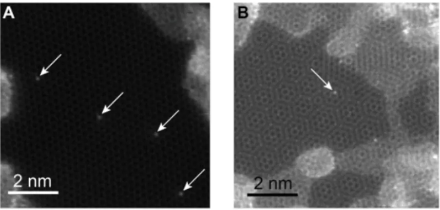
To reduce the replacement of the dopant by C, we also used double-layer graphene (Figure 2-6), where atom diffusion on one side is suppressed. It is interesting to observe that the phosphorous dopant in a double-layer graphene is much less likely to be replaced than in monolayer graphene. With a similar dose rate, the P atom was not replaced during our observation (∼12 minutes), which is more than four times longer
than in single-layer graphene (∼3 minutes). It should be noted that the difficulty of manipulating P atoms represents a generic challenge in atomic engineering, where a desired configurational outcome is degraded by other unwanted ones. Our paper is specifically focusing on dealing with this issue.
Figure 2-6: STEM MAADF images (raw data) of the single-layer and double-layer graphene area where P dopant atoms are spotted.
To explain these processes, we have performed extensive ab-initio molecular dy-namics (abMD) and climbing-image nudged elastic band (cNEB) calculations. With a clear separation of timescales, in particular 𝜏E≪ 𝜏I, it is a reasonable approximation
to simulate the configurational change processes on the BO surface assuming each dynamic step evolves according to the Hellman-Feynman forces calculated based on the electronic ground state.
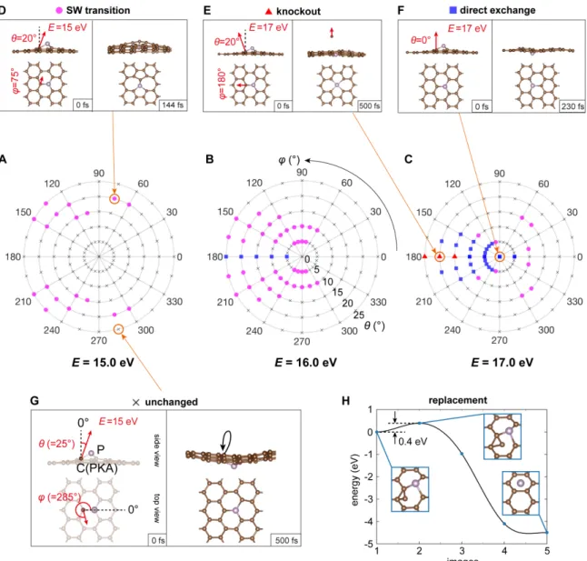
The distribution of various types of dynamics are shown in Figure 2-7(A-C), which corresponds to initial post-collision kinetic energies of the PKA at 𝐸 = 15, 16, and 17 eV, with the angular space sampled with an interval of 15° for the azimuthal angle 𝜙 and 5° for the polar angle 𝜃 (up to 25°). Figure 2-7(D-G) are four exam-ples representing different dynamical processes, shown in the order of SW transition, knockout, direct exchange, and unchanged structure. All of these beam-induced dy-namics of P dopants are initiated by an out-of-plane momentum imparted on PKA by the backscattering of a single electron, which occurs stochastically with a small probability. The definitions of spherical coordinates 𝜃 and 𝜙 (momentum direction of the PKA whose energy is 𝐸) are plotted in the first frame of Figure 2-7(G), along with
an example of an unchanged structure (𝜃 = 25°, 𝜙 = 285°, with the kinetic energy 𝐸 = 15.0 eV). If the initial velocity is not strictly upwards, but tilted at an angle (𝜃 = 20°, 𝜙 = 75°, 𝐸 = 15 eV in this case), a SW transition occurs (Figure 2-7(D)) [46]. As an example of knockout in Figure 2-7(E), the initial momentum of PKA is tilted toward 𝜃 = 20°, 𝜙 = 180°, with 𝐸 increased to 17.0 eV. Finally, in Figure 2-7(F), an initial PKA velocity perpendicular to the plane (𝜃 = 0°) yields a direct exchange when 𝐸 = 17 eV.
Figure 2-7: Mechanisms of P dopant dynamics in graphene calculated with ab-initio molecular dynamics.
From these plots, several conclusions can be drawn for the phosphorous dopant: (I) a SW transition can be initiated with a lower PKA energy 𝐸 (starting from 15 eV) than direct exchange. (II) Increasing from 15 to 17 eV, direct exchange gradu-ally becomes the dominant dynamical process. (III) When E reaches around 17 eV, knockouts begin to occur. (IV) Somewhat counterintuitively, direct exchange is eas-ier when the PKA momentum is pointing away from the target P atom (𝜙 = 180°), instead of pointing toward it (𝜙 = 0°). As we shall see, these polar plots features are predictable from the PKS theory, from which the relative scattering cross sections of each configurational outcome can be estimated.
The replacement dynamics (Figure 2-5(D)) are due to the free C adatoms on graphene surface. In Figure 2-7(H), our calculation shows that C adatoms can bond stably on a C-C bridge close to the underside of a P site (shown as the initial state). By performing a cNEB calculation, we see that to transit from this initial state to a final state where the P has been replaced by C, the system only needs to cross a 0.4 eV barrier, available thermally or from the 60 keV electron beam [50], and subsequently reducing the potential energy of the system by 4.5 eV.
Comparing different graphene dopants, we found P to hop much less actively in experiment than what has been reported for Si [43]. To explain this, we compare the PKS-predicted energy range of direct exchange for Si, P, as well as Al when assuming a head-on collision (𝜃 = 0°; Figure 2-8(A)). We find that Si clearly covers the greatest energy range, resulting in larger probability of direct exchange than for P. The displacement threshold of the C neighbor of an Al dopant is much lower than for Si and P, so knockout of the PKA is a more likely outcome for Al dopants. In fact, we have observed an Al dopant and its surrounding atoms being displaced by a 60 keV electron beam (Figure 2-8(B)), while we never observe such process for Si or P at the same electron energy. This implies that a lower acceleration voltage ( ˜𝐸e)
could help facilitate direct exchange also for Al.
On the contrary, a SW transition is more likely to be observed for a P dopant compared with Si. Related cNEB calculations are shown in Figure 2-8(C). As a broader comparison, we compute six elements, including C, N, B, P, Si, and Al, any
of which theoretically could experience a SW transition. To be able to observe the SW transition in STEM, the 55-77 structure must be sufficiently stable to capture an image frame. Its stability is proportional to the depth of the potential energy well of the 55-77 structure (energy barrier between the highest energy transition state and the 55-77 structure), which is given as the activation energy 𝐸a. We note
that the cNEB calculation can only provide qualitative ranking, not quantitative characterization of the beam-induced dynamical process, since the electron-imparted momentum is highly localized on the PKA and does not necessarily exactly follow the collective reaction pathway of the minimum energy path. The stability of 55-77 structures follows the order C>N>B>P>Si>Al. Among all the dopants we observed, we indeed find that N has the most stable 55-77 structure (Figure 2-8(D); the single-atom EELS characterization of this particular N dopant can be found in Ref. [51]). Purely thermally, for a pre-exponential factor of 2 × 10¹² /s estimated from harmonic
analysis in Ref. [52], the Si 55-77 structure back-transformation rate at 300 K is 0.073/s, making such defects (and all the dopants with higher energy barrier) in principle STEM-observable if they are created.
2.5
Primary Knock-on Space
Predicting and comparing the scattering cross sections of different dynamic processes within a unified framework is essential for atomic engineering, so we have developed a formalism, Primary Knock-on Space (PKS). Illustrated on the polar plots in Figure 2-8(A-C), the azimuthal angle 𝜙 and polar angle 𝜃 correspond to the direction of the momentum of post-collision PKA (Figure 2-9(A)), and the radius of the polar plot represents its kinetic energy E (Figure 2-9(B)). Every point in PKS describes the momentum status of the PKA in terms of its momentum direction and kinetic energy right after collision (𝑡 = 𝜏c), all of which lead to a dynamic outcome which correspond
to the points in Figure 2-7(A-C). In Figure 2-9(C), these outcomes are grouped to differently colored blocks represented in three dimensions in PKS. The momentum distribution of knock-on atom after an electron collision has an ovoid profile, whose
shape changes with respect to the energy and direction of an incoming electron and the pre-collisional momentum of the atom. This momentum distribution we conceptualize as a “Doppler Amplification Effect” because small changes in incoming momentum can lead to a much greater change of the outcoming momentum, as illustrated in Figure 2-9(B). Here only atoms vibrating perpendicular to the graphene plane are considered. The Doppler Amplification effect is essential here because our calculation show that if there were no pre-collisional kinetic energy of the atom, there would not be a chance of direct exchange, Stone-Wales transitions, or knockout of a carbon neighbor in the experiments (Figure 2-5). In Figure 2-9(C), the intersection of the colored regions and the ovoid of a vibrating carbon atom (we use ˜𝐸 = 0.5eV here for amplified illustration) interacting with a 60 keV electron is projected to the polar plot in Figure 2-5(D), where areas a, b, and c correspond to regions of counterclockwise SW transition, direct exchange, and clockwise SW transition. The existence of these three intersections imply that all of the above dynamic processes are possible when the electron beam is pointing strictly upwards (˜𝜃e = 0°), due to the possibility of the
electron scattering to an angle and transferring some lateral momentum [45,53].
2.5.1
A detailed mathematical derivation of PKS
Every point in PKS describes the momentum status of the PKA in terms of its momentum direction and kinetic energy right after collision, which can be identified by a triplet Γ ≡ (𝜃, 𝜙, 𝐸). Similarly, the energy-momentum triplet of a pre-collision electron (𝑡 = 0−) will be denoted by ˜Γ
e≡ (˜𝜃e, ˜𝜙e, ˜𝐸e) and that of a pre-collision PKA
(𝑡 = 0−) will be denoted by ˜Γ ≡ (˜𝜃, ˜𝜙, ˜𝐸). The PKS differential volume is denoted
by 𝑑Γ = 𝐸2𝑑Ω𝑑𝐸 where 𝑑Ω is the solid angle of the post-collisional PKA momentum
direction, and has unit of eV3 despite conveying momentum vector-space information
(one can think of Γ-space as a transformed momentum space with easy-to-read labels in eV).
The PKS framework involves a two-step process: (1) electron scattering from the nuclear potential of the PKA, denoted “electron→PKA” (a zeptosecond-timescale in-teraction, 𝜏c ∼ 10−22 s) and described by function 𝑄, the PKA momentum resolved
Figure 2-9: Primary Knock-on Space (PKS): a scheme for evaluating relative scatter-ing cross sections of different dynamic processes.
electron differential cross-section; (2) the ensuing dynamics of the PKA, denoted “PKA→configurational change” (a picosecond-timescale interaction, 𝜏I ∼ 10−12 s)
described by 𝑃𝑖, the probability that outcome 𝑖 will take place. For every
energy-momentum triplet Γ in PKS, the outcome functions 𝑃𝑖(Γ) describe the probability
that such a scattering event leads to an outcome configuration of unchanged (𝑖 = 0), direct exchange (𝑖 = 1), SW transition (𝑖 = 2), knockout (𝑖 = 3), etc., which is crystal-structure dependent, and with 0 ≤ 𝑃𝑖(Γ) ≤ 1 , ∑︀𝑖𝑃𝑖(Γ) = 1. Thermal and quantum
perturbations of the surrounding crystal structure can smear the branching rates and make 𝑃𝑖 neither 1 nor 0, but because 𝐸 has a much larger magnitude than such
sur-rounding fluctuations, there tends to be a dominant outcome 𝑐(Γ) ≡ arg max𝑖𝑃𝑖(Γ)
for every Γ (𝑐 stands for “configurational outcome” denoted by different colors). For example, if direct exchange is the most probable outcome at Γ, then 𝑐(Γ) = 1; if SW transition dominates at Γ, then 𝑐(Γ) = 2, etc. We will use 𝑐(Γ) to partition the PKS into different color blocks in the 3D visualization scheme shown in Figure 2-9(C) (we use blue color for 𝑖 = 1, magenta for 𝑖 = 2, etc.). Also, 𝑐(Γ) = 0 for regions where recovering to the same configuration is the dominant outcome. Different total cross sections of dynamic processes can be calculated considering the following two consec-utive processes:
“Electron→PKA” process: We introduce an intermediate function 𝑄(Γ; ˜Γe) ,
which has units of barn/eV3, to describe the probability that a single penetrating
elec-tron can eject the PKA into a particular differential PKS volume 𝑑Γ (units of eV3) by
impinging on the corresponding impact-parameter differential area 𝑑𝜎 = 𝑄(Γ; ˜Γe𝑑Γ).
𝑄is essentially a probability density distribution, partly due to the impact-parameter dependence of the electron-PKA collision, and partly due to the probabilistic nature of ˜Γ , the pre-collision PKA momentum, which has been shown to be significant and important [47,54]. 𝑄 can be computed as
𝑄(Γ; ˜Γe) =
∫︁
where ˜𝑃 (˜Γ)is the probability distribution of PKA momentum before collision (𝑡 = 0−) [47, 55], and is its differential volume. The function 𝑞(Γ, ˜Γ; ˜Γe) describes the
energy-momentum resolved cross section of PKA parameterized by ˜Γ: 𝑞(Γ, ˜Γ; ˜Γe) ≡ 1 𝐸2 𝑑2𝜎 𝑑Ω𝑑𝐸 = 1 𝐸2 𝑑𝜎 𝑑Ω(Γ, ˜Γ; ˜Γe) × 𝛿 [︁ 𝐸 − 𝑓 (𝜃, 𝜑, ˜Γ; ˜Γe) ]︁ , (2.27) where 𝑑𝜎
𝑑Ω(Γ, ˜Γ; ˜Γe) is the angular resolved differential cross section of electron-atom
scattering derived from McKinley-Feshbach formalism [47,56], 𝜎(𝜃) = 𝜎R[1 − 𝛽2sin2( 𝜃 2) + 𝜋 𝑍𝑒2 ¯ ℎ𝑐 𝛽 sin(𝜃/2)(1 − sin( 𝜃 2))] (2.28) and 𝜎R = ( 𝑍𝑒2 8𝜋𝜖0𝑚0𝑐2 )21 − 𝛽 2 𝛽4 csc 4 (𝜃/2). (2.29)
which describes the scattering probabilities of PKA with respect to its outgoing angles and energy. The delta function in energy is the result of energy-momentum conserva-tion and is independent of the details of the nuclear potential. The funcconserva-tion 𝑓 defines the energy contour of PKA with respect to the outgoing angles 𝜃, 𝜙 given the status of incident electron ˜Γe and pre-collision PKA, ˜Γ. We use a relativistic treatment to
obtain 𝑓 as shown in the following equation:
𝑓 (𝜃, 𝜙, ˜Γ; ˜Γe) = 𝐸max(sin ˜𝜃ecos ˜𝜙ecos 𝜙 sin 𝜃 + sin ˜𝜃esin ˜𝜙esin 𝜙 sin 𝜃 + cos ˜𝜃ecos 𝜃)2
+ ∆𝐸vib(𝜃, 𝜙, ˜Γ), (2.30)
where the first term accounts for the ovoid without vibration ( ˜𝐸 = 0), and the second is a correction to the first term by considering the pre-collision status of PKA (˜Γ). The above equation can be simplified for head-on collision (˜𝜃e = 0) and ˜𝐸 = 0:
𝑓 (𝜃, 𝜙, ˜𝐸 = 0; ˜𝜃e= 0) = 𝐸maxcos2𝜃. (2.31)
mo-mentum direction ˜𝜃e , ˜𝜙e, describes the scattering from the nuclear potential, and
thus does not depend on the crystal structure.
“PKA→configurational change” process: The total cross section of a dynamic process 𝑖 can then be computed by integrating 𝑄 in equation (2.26) weighted by outcome function 𝑃𝑖 over the whole PKS:
𝜎𝑖(˜Γe) =
∫︁
𝑑3Γ × 𝑃𝑖(Γ) × 𝑄(Γ; ˜Γe), (2.32)
where 𝑑3Γ ≡ 𝐸2sin 𝜃𝑑𝐸𝑑𝜃𝑑𝜙is the PKS differential volume element for post-collision
PKA. The cross sections of different dynamic processes are functions of ˜Γe, indicating
that the probabilities of different dynamics can be tuned by the energy of electron ( ˜𝐸e), or by the incident angles ( ˜𝜙e, ˜𝜃e) with respect to the sample, which can be
tuned by tilting the beam or the sample (Figure 2-10). These are the primary control variables of atomic engineering, along with the selection of the PKA.