Bright single InAsP quantum dots at telecom
wavelengths in position-controlled InP
nanowires: the role of the photonic waveguide
Sofiane Haffouz,
∗,†Katharina D. Zeuner,
‡Dan Dalacu,
†Philip J. Poole,
†Jean
Lapointe,
†Daniel Poitras,
†Khaled Mnaymneh,
†Xiaohua Wu,
†Martin Couillard,
†Marek Korkusinski,
†Eva Schöll,
‡Klaus D. Jöns,
‡Valery Zwiller,
‡and Robin L.
Williams
††National Research Council of Canada, Ottawa, Ontario, Canada, K1A 0R6. ‡KTH Royal Institute of Technology, Stockholm, Sweden
Supplementary Information
Additional PL measurements from nanowire ’ensembles’
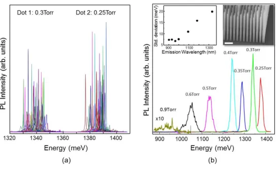
The variation in quantum dot emission energies for nominally identical dots was determined
from measurements of both individual nanowires as well as nanowire arrays. In Fig. S1(a),
the PL spectra of 50 nominally identical nanowires, each containing two dots, are shown.
This double dot sample corresponds to the sample shown in the top spectrum of Fig. 1(b).
Fig. S1(b) shows the PL spectra of nanowire arrays pitched at 400 nm (see right inset)
such that each spectrum corresponds to emission from ∼ 25 nanowires. The wavelength
dependence of the energy spread in shown in the left inset.
Figure S1: (a) PL spectra from 50 double dot nanowires. (b) PL spectra from nanowire arrays with dots grown using different AsH3 flux. Right inset show an SEM image of one of
TEM analysis of the quantum dot structure
The quantum dots were analyzed by transmission electron microscopy (TEM). The
compo-sition of thicker dots were determined from energy dispersive X-ray spectroscopy (EDX) in
scanning TEM mode (STEM). A high angle annular dark field (HAADF) STEM image of
a thick quantum dot grown using an AsH3 flow of 3 sccm and a growth time of 15 seconds
is shown in Fig. S2(b). An EDX linescan of the dot is shown in Fig. S2(b) from which a
composition of InAs0.5P0.5 is determined.
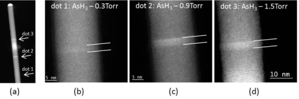
In Fig. S3 we show the analysis of a nanowire containing three thinner quantum dots
each grown with a growth time of 3.5 seconds but using different AsH3 flux. The increase in
contrast observed with increasing AsH3 flux is consistent with an increase in arsenic content
(e.g. due to the sensitivity of the detector to atomic number).
Figure S3: (a) HAADF TEM image of a nanowire containing three dots grown under different AsH3 flux. (b)-(d) High resolution TEM images of the three quantum dots.
The quantum dot thickness versus growth time was calibrated by growing three quantum
dots in a nanowire at a constant AsH3 flux of 3 sccm but for varying times. Fig. S4 shows
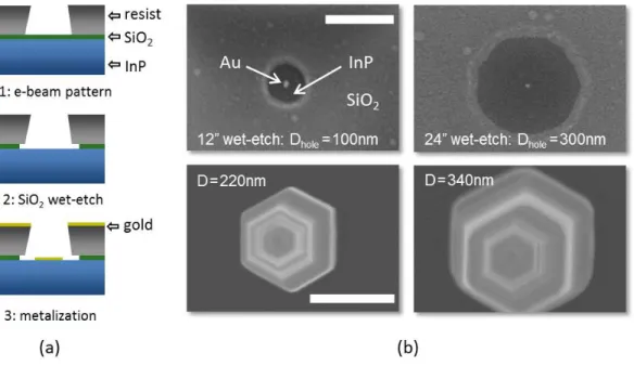
Growth substrate processing used to control waveguide diameters
The two step (core-cladding) growth process used to grow the nanowire devices allows for
independent control of the quantum dot (core) and the waveguide (cladding). Fig. S5(a)
shows schematically three of the processing steps involved in the preparation of the growth
substrate. The second step defines the opening in the SiO2 mask that permits the
selective-area growth of the cladding. The size of this opening is determined by a hydrofluoric wet-etch
which, in turn, determines the diameter of the clad nanowire. For example, by increasing
the hole diameter from Dhole = 100 nm (12 s etch) to Dhole = 300 nm (24 s etch) the diameter
of the clad nanowire increases from D = 220 nm to D = 340 nm, as shown in the upper and
lower panels, respectively, of Fig. S5(b).
Figure S5: (a) Processing steps for the preparation of the growth substrate. (b) Upper panel: SiO2 hole opening for different etch times. Lower panel: top-view SEM of nanowires grown