HAL Id: hal-01736061
https://hal.archives-ouvertes.fr/hal-01736061
Submitted on 23 Mar 2018
HAL is a multi-disciplinary open access
archive for the deposit and dissemination of
sci-entific research documents, whether they are
pub-lished or not. The documents may come from
teaching and research institutions in France or
abroad, or from public or private research centers.
L’archive ouverte pluridisciplinaire HAL, est
destinée au dépôt et à la diffusion de documents
scientifiques de niveau recherche, publiés ou non,
émanant des établissements d’enseignement et de
recherche français ou étrangers, des laboratoires
publics ou privés.
Formation and evolution of F nanobubbles in amorphous
and crystalline Si
S. Boninelli, G. Impellizzeri, S. Mirabella, F. Priolo, E. Napolitani, Nikolay
Cherkashin, Fuccio Cristiano
To cite this version:
S. Boninelli, G. Impellizzeri, S. Mirabella, F. Priolo, E. Napolitani, et al.. Formation and evolution
of F nanobubbles in amorphous and crystalline Si. Applied Physics Letters, American Institute of
Physics, 2008, 93 (6), pp.61906 - 171916. �10.1063/1.2969055�. �hal-01736061�
Formation and evolution of F nanobubbles in amorphous and crystalline Si
S. Boninelli, G. Impellizzeri, S. Mirabella, F. Priolo, E. Napolitani, N. Cherkashin, and F. Cristiano
Citation: Appl. Phys. Lett. 93, 061906 (2008); doi: 10.1063/1.2969055 View online: https://doi.org/10.1063/1.2969055
View Table of Contents: http://aip.scitation.org/toc/apl/93/6
Published by the American Institute of Physics
Articles you may be interested in
Evidences of F-induced nanobubbles as sink for self-interstitials in Si
Applied Physics Letters 89, 171916 (2006); 10.1063/1.2364271
Mechanisms of boron diffusion in silicon and germanium
Formation and evolution of F nanobubbles in amorphous and crystalline Si
S. Boninelli,1,a兲G. Impellizzeri,1S. Mirabella,1F. Priolo,1E. Napolitani,2N. Cherkashin,3and F. Cristiano4
1
MATIS CNR-INFM and Dipartimento di Fisica ed Astronomia, Università di Catania, Via Santa Sofia 64, 95123 Catania, Italy
2
MATIS CNR-INFM and Dipartimento di Fisica, Università di Padova, Via F. Marzolo 8, 35131 Padova, Italy
3
CEMES-CNRS, 29, Rue Jeanne Marvig, 31055 Toulouse, France 4
LAAS-CNRS, 7, Avenue du Colonel Roche, 31077 Toulouse, France
共Received 19 May 2008; accepted 17 July 2008; published online 13 August 2008兲
The formation and evolution of F-induced nanobubbles in Si was investigated. Si samples were preamorphized, implanted with F, and partially regrown by solid phase epitaxy共SPE兲. It is shown that nanobubbles are formed already in the amorphous side of partially regrown samples and are then incorporated in crystalline Si during SPE. The bubbles are interpreted as the result of the diffusion and coalescence of F atoms and dangling bonds already in the amorphous matrix. During high temperature annealing after SPE, F outdiffuses; correspondingly, the bubbles partially dissolve and transform from spherical- to cylinder-shaped bubbles. © 2008 American Institute of Physics. 关DOI:10.1063/1.2969055兴
In recent years, the beneficial effects of F on the reduc-tion of B transient enhanced diffusion共TED兲 in Si have been widely observed. Many efforts, both experimental and theo-retical, have been devoted to understand the F behavior in Si and different mechanisms have been proposed to explain the role of F. So far, it has been proved that the reduction of B TED cannot be ascribed to the formation of F–B complexes.1 Besides, the interaction between F and Si interstitials atoms 共Is兲 cannot be invoked to explain the beneficial effects of F in terms of stabilization of the end of range defects.2,3The formation of F-vacancies 共V兲 complexes was also proposed to explain the effect of F on the reduction of boron TED.4 Indeed, transmission electron microscopy 共TEM兲 revealed the presence of bubbles in crystalline Si 共c-Si兲 implanted with BF2+, after thermal annealing at high temperature,5,6and positron annihilation spectroscopy evidenced the presence of F-V complexes in c-Si, implanted with F.7,8 Recently, we investigated the role of F-induced bubbles on Is defects in preamorphized Si, revealing the presence, just after solid phase epitaxy共SPE兲, of a band of cavities acting as efficient traps for Si Is.9These evidences are supported by ab initio calculations, which have shown that in c-Si, F atoms prefer-entially form complexes with V 共indicated as FnVm兲, due to
their great ability in saturating Si dangling bonds 共dbs兲, rather than bind with Is or B or F.10 Indeed, the somewhat high binding energy of these FnVmconfigurations, having all
dbs decorated by F, makes them highly stable.11In literature, all experiments devoted to the understanding of the F behav-ior are done with F implanted in crystalline or preamor-phized Si matrix. The only experiment realized in amorphous Si共a-Si兲 has been conducted by Nash et al., who studied the transport of F using secondary ion mass spectrometry 共SIMS兲 and showed by TEM that F transport is influenced by F “inclusions.”12 Clearly, it is now necessary to study the generation of F bubbles in detail and to investigate their
possible formation starting from the amorphous phase. In this work, we present a study on the formation of F-induced bubbles during SPE. TEM and SIMS analyses re-veal that these bubbles already form in a-Si, in correspon-dence of the highly F enriched region. These defects are transferred into the c-Si once the amorphous-crystalline共a-c兲 interface advances. The thermal evolution of these F-induced bubbles in recrystallized sample has been investigated and their volume evaluated as a function of thermal treatments.
Silicon samples were prepared by molecular beam epi-taxy, containing a Si1−yCy layer 共y=0.005兲 at a depth of
about 800 nm. They were then amorphized from the surface to a depth of⬃1 m by Si implants共5⫻1015 ions/cm2 at 500 keV and 2⫻1015 ions/cm2at 40 keV兲 at liquid nitrogen temperature. F was then implanted in the samples with a dose of 4.4⫻1015 ions/cm2at 75 keV. Finally, samples were annealed at 450 ° C for 30 min at 700 ° C for 25, 70, or 100 s to induce partial or complete SPE regrowth. In addition, the fully regrown samples were cut into three pieces and further annealed at 800, 900, or 1000 ° C for 900 s. The Is released from the end of range defects during annealing are stopped by the Si1−yCy layer, thus being prevented from arriving at
the F-enriched region.13The TEM analyses were performed by using a 200 keV JEOL 2010-HC. The F-induced defects are bubbles, which are imaged in defocused off-Bragg bright field conditions to observe the Fresnel-fringe contrast. As this contrast depends on the abrupt change of the mean inner potential at the interface between the bubbles and the Si ma-trix, it allows the visualization of the whole population of bubbles in both a-Si and c-Si, within the detection limit of this technique 共about 2 nm兲. The atomic concentration of F was determined by SIMS, using a CAMECA IMS-4f instru-ment, with a 3 keV, O2+analyzing beam.
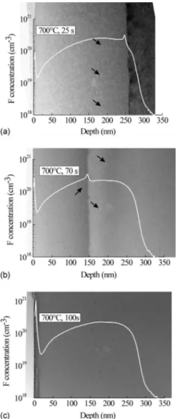
In Fig. 1, the kinetics at 700 ° C for different times of preamorphized Si implanted with F is reported. All images were obtained by cross-sectional TEM. In the sample an-nealed for 25 s关Fig.1共a兲兴 the position of the a-c interface is clearly visible at about 250 nm below the surface. A 65 nm wide band of bubbles, whose mean diameter is about 3 nm,
a兲Author to whom correspondence should be addressed. Present address: Fondazione Istituto Italiano di Tecnologia, Via Morego 30, 16163 Genova, Italy. Electronic mail: simona.boninelli@iit.it.
APPLIED PHYSICS LETTERS 93, 061906共2008兲
is present in the amorphous side centered at a depth of ⬃180 nm, while the recrystallized Si appears free of defects. After 70 s 关Fig.1共b兲兴 the a-c interface has shifted at ⬃150 nm below the surface and several bubbles with almost un-changed mean sizes, are visible both in the amorphous and crystalline sides. Finally, after 100 s关Fig.1共c兲兴 the sample is fully recrystallized and a band of larger bubbles 共6 nm in diameter兲 are observed at the same position as before. These results indicate that bubble nucleation is favored in a-Si, while bubble growth is enhanced in c-Si.
The SIMS F profile of each sample is superimposed in the cross-sectional image. It has already been shown that partially regrown samples show the characteristic F segrega-tion peak in the amorphous side of the a-c interface due to F atoms, which are forced toward the surface by the moving
a-c interface.14 Figure 1 shows that the band of bubbles is located around the maximum of the F concentration profile, clearly suggesting that the mechanism of bubble formation involves F atoms.
Our results show that bubbles form already in a-Si and
that they are incorporated in toto during SPE. Amorphous Si is represented as a tetrahedrally coordinated configuration without long-range order. The most common defects in a-Si are the threefold coordinated db and the fivefold coordinated floating bonds, represented by hybrid orbitals partially filled by unpaired electrons. It has been demonstrated that these unsaturated bonds are responsible for the passivation of Si by F.15Moreover, at high F concentration the formation of large clusters is favored, as the creation of each F-saturated db further lowers the overall energy of the system.16 This sug-gests that the early stages of such complexes formation, which prelude to the F-induced bubbles in a-Si, might be originated by the saturation of Si db by F. After the 700 ° C, 25 s annealing, these db-F complexes grow and evolve to-ward the formation of clusters, the largest of them being visible by TEM. The thermal annealing at 700 ° C for 70 s, besides favoring the proceeding of the a-c interface, pro-motes the further formation of visible bubbles still in the amorphous phase关Fig.1共b兲兴. Once formed, these bubbles are extremely stable; thus, they are incorporated directly into the
c-Si during the passage of the a-c interface.
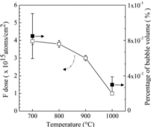
In order to investigate the thermal effect on the F bubbles, the fully regrown samples共post-SPE兲 were further annealed at 800, 900, and 1000 ° C, for 900 s. In Fig.2, plan view TEM images of the post-SPE sample关Fig.2共a兲兴 and of samples further annealed at 900 关Fig. 2共b兲兴 and 1000 °C 关Fig.2共c兲兴 are reported. The post-SPE sample shows a popu-lation of almost spherical bubbles with a mean diameter of about 6 nm. The sample further annealed at the highest tem-perature 共1000 °C兲 presents again spherical bubbles and a new feature with bubbles elongated in the 具100典 directions, as shown by the corresponding diffraction pattern reported in Fig. 2共d兲. The mean diameter of spherical bubbles is 3 nm, while the length of the cylindrical bubbles is 10 nm. The sample annealed at 900 ° C presents mainly spherical bubbles共about 80% of the total population of defects兲 with few cylindrical bubbles, denoting the transition of these de-fects from the spherical shape toward the cylindrical one. In this case, the mean diameter of the spherical bubbles is 6 nm, while the mean length of the cylindrical ones is 9 nm. Cross-sectional TEM analyses 共not shown兲 evidenced that the de-fect band enlarges from about 80 nm after SPE to about 170 nm after SPE plus 1000 ° C. Moreover, all cylindrical bubbles shown in Fig.2共c兲display the same diameter value, equal to about 2 nm. By measuring, from Figs.2共a兲and2共c兲, size and density of spherical and cylindrical defects, the per-centage of volume occupied by the bubbles 共in the region where bubbles are present兲, was evaluated as function of the thermal treatment. The results, reported in Fig. 3共right
ver-tical axis兲, show that the percentage of volume occupied by the bubbles decreases from 0.085% after SPE to 0.030% after SPE plus 1000 ° C. These observations suggest that the cylindrical bubbles are the result of a nonconservative evo-lution, where the spherical bubbles modify themselves after SPE and the length of the cylinders progressively increase. Moreover smaller bubbles, not visible by TEM, are presum-ably present already after SPE also in regions with a lower F concentration and grow during post-SPE high temperature annealing forming visible bubbles and producing the ob-served enlargement of the defect band.
In Fig. 3 共left vertical axis兲, we reported the F dose
re-tained in the samples for different thermal treatments, as
FIG. 1. SIMS F concentration profile overlapped with TEM cross-sectional view of samples implanted with F and partially regrown by SPE at 700 ° C for 共a兲 25 s and 共b兲 70 s. In 共c兲 the fully regrown sample, after 100 s annealing, is reported. In共a兲 and 共b兲, the arrows point to some bubbles. The different contrast shown by bubbles in共a兲 and 共b兲 with respect to 共c兲 de-pends by the different over- and under-focus imaging conditions used.
measured by SIMS. In detail, the F dose reduces from 4⫻1015 atoms/cm2 after SPE to 1⫻1015 atoms/cm2 after SPE plus 1000 ° C. By comparing the TEM and SIMS re-sults, it is possible to state that in c-Si, while F partially evaporates from the surface, the total volume occupied by bubbles proportionally reduces. Hence we can conclude that bubbles are not only formed but also stabilized by the pres-ence of F, as, once F evaporates, the bands are rearranged and the bubble volume proportionally decreases.
In conclusion, the investigation of F-induced bubble for-mation in Si during SPE clearly shows the appearance of precursors already in the amorphous phase. This evidence was interpreted in terms of passivation of Si db by F. The growth and coalescence of these F-db complexes lead to the
formation of bubbles in the amorphous phase, which are di-rectly transferred in the crystal. Finally we demonstrated that after high temperature annealing a large part of F evaporates from the surface and, at the same time, the defect volume proportionally reduces. These results have important impli-cations for the modeling of F behavior during SPE and its incorporation in c-Si, and for its use for point defect engi-neering in ultrashallow junctions.
We wish to thank C. Percolla and S. Tatì 共MATIS CNR-INFM兲, A. Marino 共IMM-CNR兲 R. Storti 共University of Padova兲, J. Crestou, and C. Crestou 共CEMES-CNRS兲 for technical support. Work at CNRS was partially supported by ESTEEM IP3 project.
1G. Impellizzeri, J. H. R. dos Santos, S. Mirabella, F. Priolo, E. Napolitani, and A. Carnera,Appl. Phys. Lett. 84, 1862共2004兲.
2D. F. Downey, J. W. Chow, E. Ishida, and K. S. Jones,Appl. Phys. Lett.
73, 1263共1998兲.
3S. Boninelli, F. Cristiano, W. Lerch, S. Paul, and N. E. B. Cowern, Elec-trochem. Solid-State Lett. 10, H264共2007兲.
4M. Diebel, S. Chakravarthi, S. T. Dunham, C. F. Machala, S. Ekbote, and A. Jain, MRS Symposia Proceedings No. 765共Materials Research Society, Pittsburgh, 2003兲, p. D6.15.1.
5J. Narayan, O. W. Holland, W. H. Christie, and J. J. Wortman,J. Appl. Phys. 57, 2709共1985兲.
6C. W. Nieh and L. J. Chen,Appl. Phys. Lett. 48, 1528共1986兲. 7X. D. Pi, C. P. Burrows, and P. G. Coleman,Phys. Rev. Lett. 90, 155901
共2003兲.
8P. J. Simpson, Z. Jenei, P. Asoka-Kumar, R. R. Robison, and M. E. Law, Appl. Phys. Lett. 85, 1538共2004兲.
9S. Boninelli, A. Claverie, G. Impellizzeri, S. Mirabella, F. Priolo, E. Na-politani, and F. Cristiano,Appl. Phys. Lett. 89, 171916共2006兲.
10G. M. Lopez, V. Fiorentini, G. Impellizzeri, S. Mirabella, and E. Napoli-tani,Phys. Rev. B 72, 045219共2005兲.
11M. Diebel and S. T. Dunham,Phys. Rev. Lett. 93, 245901共2004兲. 12G. R. Nash, J. F. W. Schiz, C. D. Marsh, P. Ashburn, and G. R. Booker,
Appl. Phys. Lett. 75, 3671共1999兲.
13E. Napolitani, A. Coati, D. De Salvador, A. Carnera, S. Mirabella, S. Scalese, and F. Priolo,Appl. Phys. Lett. 79, 4145共2001兲.
14S. Mirabella, G. Impellizzeri, E. Bruno, L. Romano, M. G. Grimaldi, F. Priolo, E. Napolitani, and A. Carnera, Appl. Phys. Lett. 86, 121905
共2005兲.
15B. R. Weinberger, H. W. Deckman, E. Yablonovitch, T. Gmitter, W. Kobasz, and S. Garoff,J. Vac. Sci. Technol. A 3, 887共1985兲.
16G. M. Lopez and V. Fiorentini,Appl. Phys. Lett. 89, 092113共2006兲. FIG. 2. Plan view images of the共a兲 sample completely regrown by SPE
共700 °C, 100 s兲 and for post-SPE samples further annealed for 900 s at 共b兲 900 ° C and 共c兲 1000 °C. In 共b兲 few elongated bubbles are indicated by circles.
FIG. 3. Behavior of total volume occupied by bubbles per defect band volume共right vertical axis兲 and dose of incorporated F 共left vertical axis兲 as a function of the post-SPE annealing temperature.