Circuits and Passive Components for
Radio-Frequency Power Conversion
by
Yehui Han
B.S., Tsinghua University (2000) M.S., Tsinghua University (2002) ASSACHUSETTS INSTitUTE OF TECHNOLOGYFEB 2 3 2010
LIBRARIES
Submitted to the Department of Electrical Engineering and Computer Science in partial fulfillment of the requirements for the degree of
Doctor of Philosophy
at the
ARCHNES
MASSACHUSETTS INSTITUTE OF TECHNOLOGY
February 2010
@
Massachusetts Institute of Technology, MMX. All rights reserved.Author
Certified by
Department of Electrical Engineering and Computer Science December 21, 2009
David J. Perreault Associate Professor of Electrical Engineering
Thesis Supervisor
Accepted by
Terry Orlando Chairman, Department Committee on Graduate Students
Circuits and Passive Components for Radio-Frequency Power Conversion
byYehui Han
Submitted to the Department of Electrical Engineering and Computer Science on December 21, 2009, in partial fulfillment of the
requirements for the degree of Doctor of Science
Abstract
T
HIS THESIS focuses on developing technology for high efficiencypower converters op-erating at very high frequencies. The work in the thesis involves
two aspects of such converters: rf (radio-frequency) power circuit design techniques and magnetic material char-acterization and application. In the aspect of circuit design techniques, the thesis investi-gates a new class of matching networks that overcomes a major limitation of rf converter circuits - their high sensitivity to loading condition. These networks, which are termed resistance compression networks, serve to substantially decrease the variation in effective resistance seen by a tuned rf inverter as loading conditions change. The thesis explores the operation, performance characteristics, and design of these networks, and present ex-perimental results demonstrating their performance. The thesis also presents analysis and design considerations for lumped (inductor and capacitor) matching networks operating at high efficiency (> 95%). Formulas for calculating matching network efficiency are given and used to evaluate the optimum number of matching stages as a function of conversion ratio. Both simulation and experimental results are presented that validate the analytical formulation.
In the aspect of magnetic materials and applications, the thesis investigates the loss char-acteristics of several commercial rf magnetic materials for power conversion applications in the 10 MHz to 100 MHz range. A measurement method is proposed to identify loss charac-teristics of different commercial rf magnetic core materials. The loss characcharac-teristics of these materials, which have not previously been available, are illustrated and compared in tables and figures. Based on results in characterization of magnetic materials, the thesis describes a procedure for magnetic components design with low permeability magnetic materials that is for very high frequency power conversion applications. This procedure provides a method to compare and evaluate different magnetic materials for given specifications of a magnetic-core inductor. Some important information, e.g. quality factor and size of the inductor can be predicted before the final design. The thesis also investigates some problems such as optimization of a magnetic-core inductor.
Thesis Supervisor: David J. Perreault
Dedication
Acknowledgements
I still remember the first day I came to MIT six years ago. In a rainy afternoon, I was led by Marilyn Pierce, our graduate administrator, walked through the underground maze from the building 38 to building 10, and met my thesis advisor, Prof. David Perreault, in his office. At that time, facing a totally different environment, I was afraid of not only getting lost at MIT buildings, but also getting lost of the direction of my PhD study. Dave's great enthusiasm, tremendous knowledge and wonderful ideas in power electronics led me walk through the maze and helped me to continue my career in academics. I feel extremely blessed to be working with such a caring advisor. I want to thank Dave for his guidance, patience and support during this academic journey.
I would like to thank my thesis committee: Prof. John Kassakian, Prof. Steve Leeb, and Prof. Charlie Sullivan. This thesis would not have been possible without their advice and support. I would also like to thank Prof. Tomas Palacios, who gave me a lot of knowledge about compound devices, and Prof. Markus Zahn, who lent his Ansoft software to me. Many thanks go to my sponsors who made this thesis possible: DARPA, General Electric, Sheila and Emmanuel Landsman, National Science Foundation, National Semiconductor, the MIT Automotive Consortium, and the MIT Center for Integrated Circuits and Systems (CICS).
I would like to show my gratitude to alumni, students and staff from LEES and our group including Al-Thaddeus Avestruz, Grace Cheung, David Giuliano, Jingying Hu, David Jack-son, Olivia Leitermann, Wei Li, Vivan Mizuno, Timothy Neugebauer, Joshua Phinney, Brandon Pierquet, Robert Pilawa, Yihui Qiu, Juan Rivas, Wayne Ryan, Anthony Sagneri, Riccardo Signorelli, Makiko Wada, Jiankang Wang, and many others.
Thanks to students that took 6.334 during the spring semesters of 2004, 2006 and 2007. Thanks to my colleagues at MIT and Tsinghua University and my friends in America and China. I would like to single out for special thanks Guang Han, roommate in college, best man at my wedding, and a great engineer.
Finally, I owe my deepest gratitude to my parents. I would not be where I am today, without their love, encouragement and support. It is my wife Xin Wang that this thesis is dedicated. I am grateful to express my gratitude to her that has been with me throughout this academic journey, providing love, support, and joyful company.
Contents
1 Introduction
1.1 Background and Motivations . . . . 1.2 Challenges of Radio-Frequency Power Conversion . . . . 1.3 Thesis Objectives and Contributions . . . . 1.4 Organization of Thesis . . . .
2 Resistance Compression Networks for Radio-Frequency Power sion
2.1 Background . . . . 2.2 Resistance Compression Networks . . . . 2.3 Resistance-Compressed Rectifiers . . . . 2.4 Design Considerations for Resistance Compression Networks . . . . 2.5 Motivation and Example Application: a 100 MHz dc/dc Converter
2.5.1 M otivation . . . . 2.5.2 Example Application . . . . 2.6 Behavior of "Phase Compression" Effect... . . . . 2.7 Conclusion . . . .
3 Analysis and Design of High Efficiency Matching Networks 3.1 Background... . . . . . . . . 3.2 Matching Network Design and Efficiency Analysis . . . . 3.3 Calculation and Simulation Results... . . . . 3.4 Experimental Results . . . . 3.5 C onclusion . . . . 21 . . . . . 21 . . . . . 22 . . . . . 24 . . . . . 25
Conver-Contents
4 Evaluation of Magnetic Materials for Very High Frequency Power
Appli-cations 73
4.1 Background ... ... 73
4.2 Measuring the Quality Factor of RF Inductors ... ... 74
4.2.1 Measurement Circuit and Principles.... . . . . . . . 74
4.2.2 Measurement Procedures... . . . .. 76
4.3 Extraction of Loss Characteristics of Commercial RF Magnetic Cores . . . 79
4.3.1 Design and Fabrication of Low-loss Inductors with Toroidal Cores . 80 4.3.2 The Extraction of Core Loss Characteristics from the Measurement R esults . . . . 81
4.3.3 The Estimation of Errors.. . . . . . . . 82
4.4 Core Loss Measurements in Commercial Magnetic Materials . . . . 83
4.5 Application Example... . . . . . . . . . . . . . 84
4.6 Conclusion . . . . 92
5 Inductor Design Methods with Low-permeability RF Core Materials 93 5.1 Background . . . . 93
5.2 Inductor Design Considerations and Questions . . . .... 5.2.1 Inductor Design Considerations . . . . 5.2.2 Inductor Design questions . . . . 5.3 Inductor Design Procedure and Methods . . . . 5.3.1 Inductor Design Procedure . . . . 5.3.2 Method to Select Among Magnetic Materials . . . . 5.3.3
QL
Estimation with Given Maximum Inductor Size 5.3.4 Size Estimation with Given MinimumQL
- -... 5.3.4.1 Step I: Calculate Coreless Design . . . . 5.3.4.2 Step II: Evaluate Magnetic Materials . 5.3.4.3 Step III: Scaling . . . . 5.3.4.4 Step IV: Check Design Assumptions . . . . 5.3.4.5 Inductor Scaling with Multi-choice of Magnetic Materials 5.3.5 Inductor Design with the Best Magnetic Material . . . . . . . . . . 95 . . . . 95 . . . . 96 . . . . 97 . . . . 97 . . . . 98 . . . . 103 - - - 104 . . . . 105 . . . . 106 . . . . 107 . . . . 108 109 111Contents
5.3.6 Relationship between Quality Factor QL and Inductor Size . . . . . 112 5.4 Optimization of Magnetic-core Inductors . . . . 113 5.4.1 Optimization of di at Fixed do and h . . . . 115 5.4.2 For a Constant Volume V, Optimization of Dimensions do, di and h 117 5.5 Approximations Used in the Proposed Methods . . . . 119 5.6 Experimental Verification . . . . 120 5.7 Conclusion ... .. . . . . . . . . 123
6 Summary and Conclusions 125
6.1 Thesis Sum m ary . . . . 125 6.2 Thesis Conclusion .. . . . . . . . 126 6.3 Recommendations for Future Work . . . . 128
A Layout of Four-element Compression Network 131
B Layout of Back-to-back Matching Network 133
C Layout of the Circuit for Measuring Inductor Quality Factor 135
D Finite Element Simulations of Copper Loss of a Magnetic-core Inductor 137
List of Figures
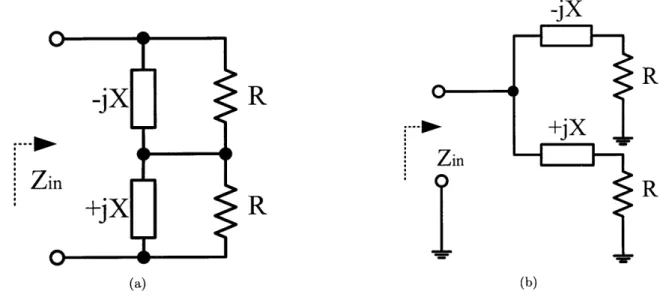
1.1 Structure of the power stage of a resonant dc/dc converter. The converter comprises an inverter (dc/ac) circuit, a transformation/matching circuit, and a rectifier (ac/dc) circuit. . . . . 21 2.1 Resistance compression circuits. Each of these circuits provides a
compres-sion in apparent input resistance. At the resonant frequency of the LC tank the input resistance R,, varies over a narrow range as the matched resistors R vary over a wide range (geometrically centered on the tank characteristic impedance). The circuits achieve lossless energy transfer from the input port to the resistors R . . . . . 29 2.2 Structure of the two basic resistance compression networks introduced in
the chapter. The impedance of the reactive networks is specified at the desired operating frequency. Implementation of the reactive networks may be selected to provide desired characteristics at frequencies away from the operating frequency. . . . . 31 2.3 Magnitude of the input resistance R{Zi,} and phase of the input impedance
(experimental and simulated) of the compression network shown in Fig. 2.1(a) as a function of R. L is a Coilcraft 100 nH coreless inductor plus 7.2 nH of parasitic inductance while C is a 33 pF mica capacitor. Measurements made at 85.15 M H z. . . . . . . . . 31 2.4 Four element compression networks. These networks can provide both
resis-tance compression and impedance transformation... . . . . . . ... 32 2.5 Four element compression network used to obtain experimental data. Layout
of this circuit is illustrated in Appendix A. . . . . 34 2.6 Four element compression network used to obtain experimental data. Layout
of this circuit is illustrated in Appendix A. . . . . 35 2.7 Input resistance (RJi{Zin}) and impedance phase (experimental and
simu-lated) of the four element compression network shown in Fig. 2.6 as a function of R. Cx = 15 pF, Lx = 169 nH, Cy = 11 pF, Ly = 246 nH; measurements m ade at 97.4 M Hz. . . . . 35 2.8 A resistance compression network with unequal loads. The load resistors are
List of Figures
2.9 Half-wave rectifier with constant voltage load and driven by a sinusoidal current source. ... ... 38 2.10 Characteristic waveforms of the half-wave rectifier shown in Fig. 2.9. The
input current and the fundamental of the input voltage are in phase. ... 38 2.11 A two element compression network with reactive branches represented by
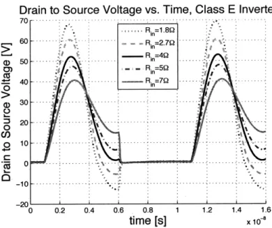
impedances evaluated at the operating frequency . . . . 39 2.12 Drain to source voltage for a class E inverter for different values of resistance.
Using the notation in [1] Li = 538 nH, L2 = 24.2 nH, C1 = 120 pF
(non-linear), C2 = 163.5 pF, 1.8 Q < R < 7 Q. Optimal zero-voltage switching (ZVS) occurs at R = 4 Q. When the resistor deviates from its nominal value
ZVS is not achieved. . . . . 43 2.13 Drain to source voltage, inverter output voltage, and gate to source voltage
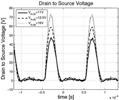
of the prototype converter... . . .. 45 2.14 Drain to source voltage for different input voltages in the range 11 V <
Vin dc < 16 V. The inverter is seen to maintain soft switching over the full
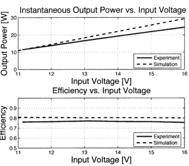
range. ... ... ... ... 46 2.15 Experimental and simulated output power and efficiency vs. input voltage.
Simulations were carried out using PSPICE. The MOSFET was modeled as switched resistor in parallel with a nonlinear capacitor, and the on-state of the diode was modeled with a constant voltage drop plus a series of resistance. Inductor ac and dc ESR values were modeled, while capacitors were treated as ideal. ... ... 47 2.16 A 100 MHz dc/dc power converter incorporating a resistance compression
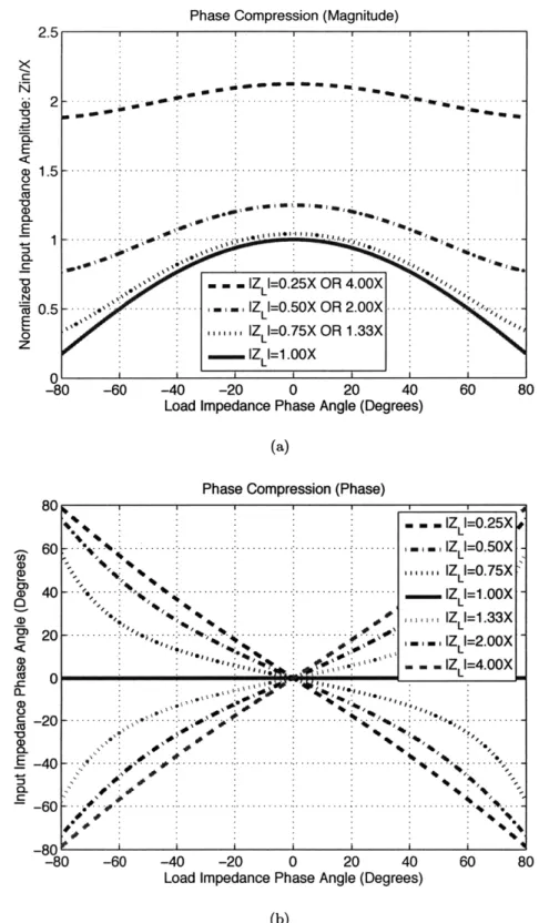
netw ork. . . . . 47 2.17 Prototype dc/dc power converter. . . . . . 48 2.18 Impedance compression networks terminated in matched non-resistive loads 49 2.19 Zin vs load impedance phase a, parameterized in load impedance magnitude
IZLI
for the topology of Fig. 2.18(a) . . . . 502.20 Zin vs load impedance phase a, parameterized in load impedance magnitude
IZLI
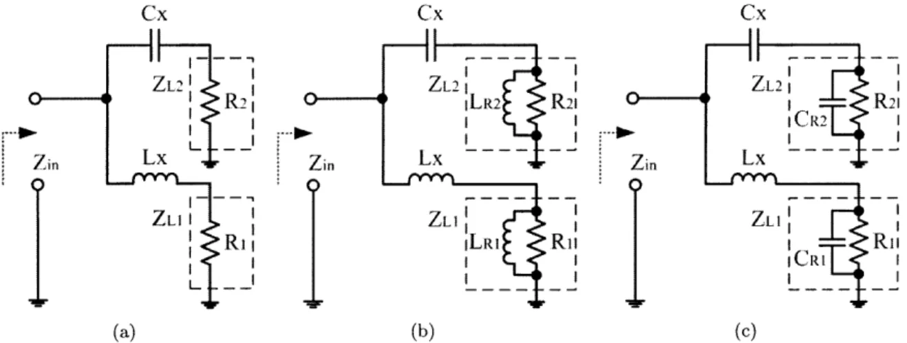
for the topology of Fig. 2.18(b) . . . . 522.21 Topologies of experimental compression networks for testing phase compres-sion effects. The load impedances are purely resistive in (a). Complex load impedances ZLi and ZL2 in (b) and (c) are achieved by parallel combinations of resistors and reactive components. . . . . 53
3.1 L-section matching networks with inductor parasitic resistance shown explicitly. 58 3.2 A multi-stage matching network.. . . . . . . . . 62
List of Figures
3.3 Optimum number of stages vs. transformation ratio. . . . . 63
3.4 Matching network efficiency vs. transformation ratio V/Vs. . . . . 64
3.5 Matching network efficiency vs. inductor quality factor. . . . . 65
3.6 Experimental setup for validating matching network efficiency calculations. Equipment and component values are detailed in Tables 3.4 and 3.5. The 50 Q power meter can be placed in either location indicated, as described in the experimental methods... . . . . . . . . . . . . 67
3.7 Experimental back-to-back matching network cascade used in the setup of Fig. 3.6. The illustrated circuit has a voltage transformation ratio to the intermediate node of 4.27 : 1. (Layout information for this circuit is presented in A ppendix B .) . . . . 68
4.1 Schematic of the circuit for measuring inductor quality factor, which can be calculated as the amplitude ratio Votpk over Vin-pk. . . . . 75
4.2 The QL of an inductor fabricated with an M3 toroidal core (OD = 12.7 mm, ID = 7.82 mm, Ht = 6.35 mm) with N = 5 turns of 116 mil wide and 4 mil thick foil, and L = 190 nH. . . . . 79
4.3 An example of an inductor fabricated from copper foil and a commercial m agnetic core. . . . . 81
4.4 M3 material core loss vs ac flux density. . . . . 84
4.5 P material core loss vs ac flux density. . . . . 85
4.6 67 material core loss vs ac flux density. . . . . 85
4.7 N40 material core loss vs ac flux density. . . . . 86
4.8 -17 material core loss vs ac flux density. Note that because the permeability of this material is low (p, = 4), it is difficult to separate core loss from copper loss. Consequently, the core was operated at extremely high loss densities under forced convection cooling in order to facilitate separation of core loss from copper loss. In many practical designs, one might choose to operate at lower loss densities than utilized here. . . . . 86
4.9 Class '12 inverter. Ls is a resonant inductor. . . . . 87
4.10 The QL of fabricated inductor withan N40 toroidal core (OD= 12.7 mm, ID= 6.3 mm, Ht= 6.3 mm) with N = 4 turns, and L = 230 nH. . . . . 89
4.11 Photographs of the 42 inverter prototype before (a, c) and after (b, d) re-placement of the coreless inductor with a magnetic-core inductor. . . . . 90
4.12 Drain to source voltage Vs and inverter load voltage VLOAD for the D2 inverter with coreless and magnetic-core inductors Ls. . . . . 90
List of Figures
5.1 Inductor design procedure . . . . 98
5.2 Inductor design example (OD= 12.7 mm, ID= 6.3 mm, Ht= 6.3 mm, L = 200 nH, Ipk = 2 A,
fs
= 30 MHz and Bpkair = 13 G). . . . . 1015.3 Inductor design example including the power loss characteristic of a coreless inductor (OD= 12.7 mm, ID= 6.3 mm, Ht= 6.3 mm, L = 200 nH, pk = 2 A,
f,
= 30 MHz and Bpk-,air 13 G). . . . . 1035.4 Inductor design example including the copper loss characteristic of a magnetic-core inductor (OD= 12.7 mm, ID= 6.3 mm, Ht= 6.3 mm, L = 200 nH, Ipk = 2 A,
fs
= 30 MHz and Bpk-air = 13 G). . . . . 1045.5 Loss plots of inductor design scaling example (OD= 12.7 mm, ID= 6.3 mm, Ht= 6.3 mm, L = 200 nH, Ipk = 2 A,
f,
= 30 MHz and Bpk-air = 13 G). . 106 5.6 The magnetic-core inductor after scaling design . . . . 1095.7 Loss plots of inductor design scaling example (OD= 12.7 mm, ID= 6.3 mm, Ht= 6.3 mm, L = 200 nH, Ipk = 0.5 A,
f,
= 30 MHz and Bpk-air = 3.2 G). 110 5.8 The magnetic-core inductor after scaling design . . . .1115.9
QL
vs. A for coreless inductor and magnetic-core inductors in different mangetic materials (L = 200 nH, Ipk = 2 A andf
= 30 MHz). At A = 1, the coreless inductor has the dimensions OD= 12.7 mm, ID= 6.3 mm and H t= 6.3 m m . . . . 1145.10 Plot of core power loss dissipation in a rectangular cross-section toroidal core as a function of normalized to that with -' = 0.5. Results are parameterized in Steinmetz parameter 3. It can be seen that over a wide range of 3, - = 0.5 is very close to the optimum, and that results are not highly sensitive to ... . . . .. 116
5.11 Core loss optimization for a constant volume. . . . . 118
5.12 The error of average flux density approximation. . . . . 120
A.1 The layout of four element compression network test board, top (Fig. A.1(a)) and bottom (Fig. A.1(b)). This layout associated with Fig. 2.6 and Fig. 2.7. 131 A.2 The compression network and rectifier PCB layout, top (Fig. A.2(a)) and bottom (Fig. A.2(b)). This layout associated with Fig. 2.16 and Fig. 2.17 [2]. 132 B.1 Back-to-back matching network PCB schematic. . . . . 133
B.2 Back-to-back matching network PCB board. Top layer.. . . . . . . . . 134
B.3 Back-to-back matching network PCB board. Bottom layer. . . . . 134
List of Figures
C.2 Circuit for measuring inductor quality factor PCB. Top layer. . . . . 136 C.3 Circuit for measuring inductor quality factor PCB. Bottom layer. . . . . 136 D.1 2D model of copper-foil windings on the top and bottom surfaces of an inductor. 138 D.2 2D model of copper-foil windings on the inner and outer surfaces of an inductor. 138
List of Tables
2.1 2.2 2.3 2.4 2.5 2.6 2.7Characteristics of the resistance compression network of Fig. 2.1(a). Components used to obtain data in Fig. 2.3. . . . . Components used to obtain data in Fig. 2.7. . . . . Components used in 100 MHz dc/de converter of Fig. 2.16. . . . . . The 0 ranges for different
|ZLI
values and a ranges. . . . . The values of components used to obtain data in Table 2.7 . . . . . Calculated and measured impedances at a frequency of 100 MHz . . 3.1 Component values for the matching networks of Fig. 3.1(a) and Fig. 3.1(b)for R, = 50 Q and R, = 3.125 Q. . . . . 3.2 Component values for the multi-stage matching network in Fig. 3.2 for R, =
50 Q and R, = 3.125 Q. . . . . 3.3 Calculated and simulated results for the matching networks in Fig. 3.1 and
F ig . 3 .2. . . . . 3.4 Equipment used in the experimental setup of Fig. 3.6. . . . . 3.5 Component types and values for the experimental matching network cascade
used in the test setup of Fig. 3.6. Measured values for circuit-board parasitics are also indicated. All measured values were obtained at a frequency of 50 MHz using an Agilent 4395A network/spectrum/impedance analyzer. . . 3.6 Experimental results for the matching network cascade with an intermediate
voltage transformation Ratio Vp/V = 3.00. . . . . 3.7 Experimental results for the matching network cascade with an intermediate
voltage transformation ratio Vp/V = 4.27. . . . . 4.1
4.2 4.3
Materials, suppliers and specifications . . . . Steinmetz parameters for materials . . . . . . . .. Comparison between the coreless inductor and magnetic-core inductor . . . 5.1 Comparison of scaling factor A among magnetic-core inductors built by P, M3 and N40 materials and designed at Ipk = 0.5 A and
fs
= 30 MHz. . . .. . . . 29 . . . . 32 . . . . 34 . . . . 54 . . . . 55 . . . . 55 . . . . 55 65 66 66 67 69 70 71 84 87 91 110
List of Tables
5.2 Comparison among coreless inductors and magnetic-core inductors designed at Ipk = 2 A and
f
8 30 MHz in different magnetic materials. . . . . 121 5.3 Magnetic-core inductor designed at L = 200 nH, Ipk = 0.5 A andf
8 =30 MHz with the scaling factor A = 0.77. . . . . 122 5.4 Magnetic-core inductor designed at L = 200 nH, Ipk = 2 A and
fs
= 30 MHzwith the scaling factor A = 0.5. . . . . 122 D.1 Finite simulation results of copper losses of a coreless inductor and
Chapter 1
Introduction
1.1
Background and Motivations
A
PRINCIPAL
means for improving performance and reducing the size of powerelectron-ics is through increasing the switching frequency. An increased
switching frequency can lower the requirement of passive components for a certain power level, and both the value and size of passive components may be reduced [3]. Resonant dc/dc power converters en-able much higher switching frequencies than can be achieved with conventional pulse-width modulated circuits, due to their natural soft-switched operation and ability to absorb and utilize circuit parasitics in the conversion process. For example, efficient resonant dc/dc power conversion has been demonstrated at frequencies in excess of 100 MHz, and opera-tion at much higher switching frequencies is clearly feasible [4-7]. Further development of resonant power converter technology is thus of great potential value.
Figure 1.1 shows a basic structure for a high-frequency resonant dc/dc converter, comprising an inverter stage, a transformation stage, and a rectifier stage [4,5,8-15]. The inverter stage draws dc input power and delivers ac power to the transformation stage. Inverters suitable for extremely high frequencies operate resonantly, and take advantage of the characteristics of the load to achieve zero-voltage switching (ZVS) of the semiconductor device(s) [16-23].
Vinc
RL
Inverter
Matching
Rectifier
Network
Figure 1.1: Structure of the power stage of a resonant dc/dc converter. The converter comprises an inverter (dc/ac) circuit, a transformation/matching circuit, and a rectifier (ac/dc) circuit.
Introduction
The rectifier stage takes ac power from the transformation stage and delivers dc power to the output. In addition to conventional rectifier topologies, resonant converters can take advantage of a variety of resonant rectifiers (e.g. [24,25]). The system may be designed such that the rectifier stage appears resistive in a describing function sense (e.g., [4, 15, 24, 25]) and is matched to the inverter by the action of the transformation stage.
Depending on the details of the converter design, the functions of the transformation stage may include matching impedances, transforming voltage and current, providing electrical isolation and providing filtering. For some high-frequency resonant inverter topologies which are highly sensitive to loading conditions, the transformation may also serve to reduce the load sensitivity of the resonant inverter [26, 27]. The transformation stage can be realized using conventional transformers and/or resonant transformers [28], transmission-line transformers [29-31], matching networks [32-34], or other similar means. In realizing these functions, a transformation circuit should ideally have a high efficiency (> 90%), require fewer passive components and have a small profile.
Power or output control of resonant converters can be achieved through a number of means, including frequency modulation [8,10, on/off control [4,6,7,35-43], and extensions of these techniques [4, 35, 44]. Fixed-frequency control techniques are preferable for systems using resonant gating [4,36, 37, 39,40,45] and in circuit implementations with high-order tuned tanks or narrow-band transformation stages. This thesis focuses primarily on designs with fixed-frequency on/off control operation.
Resonant converters utilize magnetic components (inductors and transformers) to realize intermediate energy storage, impedance transformation, soft switching, resonant rectifica-tion, and filtering. These magnetic components are operating at high flux levels, and often under large flux swings. Moreover, it would be desirable to have improved magnetic com-ponents for rf circuits such as matching networks [32-34, 46, 47].There is thus a need for magnetic materials and components suitable for operation under high flux swings at fre-quencies above 10 MHz. Small, high efficiency magnetic components are required to realize rf power converters, and there is a particular need to achieve high quality factor at radio frequencies for resonant magnetic elements.
1.2
Challenges of Radio-Frequency Power Conversion
The subject of this thesis is the miniaturization of power electronics. Increasing switching frequency dramatically is a substantial means to improve size and performance of power electronics systems. However, the switching frequency is difficult to increase because there
1.2 Challenges of Radio-Frequency Power Conversion
are many challenging issues in aspects of circuit design and passive components, especially magnetics. These challenges are outlined in this section.
A major limitation of resonant converter circuits is the sensitivity of the inverter stage to the variations of load. It has been reported that switched-mode rf inverters suitable for ultra-high frequencies (e.g., classes DE, E, F, <b and so forth) are ultra-highly sensitive to the effective impedance of the load. For example, conventional class E inverters only operate under the desired ZVS condition over about a factor of two in load resistance [26,27]. While acceptable in communications applications (in which the load resistance is relatively constant), this is problematic for many dc-dc power converter applications, where the effective resistance [15] presented by the matching stage and rectifier varies greatly with input/output voltage and current. This problem is particularly severe in applications in which the voltage conversion ratio varies substantially; such applications include charging systems where the converter must deliver constant power over a wide output voltage range and regulating converters where the converter must operate over a wide input voltage range. This thesis introduces a new circuit technique that overcomes one of the major limitations of resonant dc/dc converters at extremely high frequencies, and expands the range of applications for which resonant conversion is effective.
A matching network is a passive two-port circuit designed to provide narrow-band impedance, current and voltage transformation between the two ports. While most widely associated with communications applications [32,33,46], matching networks also find useful applica-tion in resonant inverters, rectifiers, and dc-dc converters. Most analytical descripapplica-tions of matching networks are based on the assumption of no loss. Where efficiency is con-sidered [4], it is typically treated as secondary to other performance goals, in accordance with the needs of communications applications. Moreover, literature focusing on the design of matching networks for very high efficiencies (e.g., 95%) appears to be lacking. In the thesis, the author presents analysis and design considerations for high efficiency (> 95%) lumped-element matching networks.
While coreless magnetics can be used at rf frequencies [47], cored magnetics offer the possi-bility of smaller size and better shielding. High frequency, low loss magnetic materials are thus of great potential value. Unfortunately, most magnetic materials exhibit unacceptably high losses at frequencies above a few Megahertz. Good rf magnetic materials, however, are not common. Moreover, the few available bulk magnetic materials which are potentially suitable for frequencies above 10 MHz are typically only characterized for small-signal drive conditions, and not under the high flux-density conditions desired for power electronics. In particular, there is a lack of information about core loss characteristics at high flux swing for such materials. This motivates better characterization of magnetic materials for high frequency power conversion applications.
Introduction
Besides of characterization of magnetic materials, it appears to be lacking of a fast and convenient inductor design procedure with low permeability magnetic material. For the same design specification, different magnetic materials may be operating under different ac flux density and their permeability and loss characteristics are significantly different. Without a fast and convenient design procedure, an individual inductor has to be designed for each magnetic material and each available core size before their final performance can be compared. If there are hundreds of material core size combinations available, there will be a lot work for the designer.
1.3
Thesis Objectives and Contributions
The thesis mainly focuses on developing technology for high efficiency power converters operating at very high frequencies. The research work in the thesis involves two aspects of such converters: rf power circuit design techniques and magnetic material characterization and application. In the aspect of circuit design techniques, the author investigates a new class of matching networks that greatly reduces the load sensitivity of resonant inverters and rf power amplifiers. These networks, which are termed resistance compression net-works, serve to substantially decrease the variation in effective resistance seen by a tuned rf inverter as loading conditions change. Compression networks ideally act without loss, such that all energy provided at the input port is transformed and transferred to the resistive load. Although resistance compression networks are a kind of matching network and can provide impedance transformation, the main purpose of these networks is for compressing the effective load resistance range as operating conditions vary. This effect can be used to overcome one of the major deficiencies of tuned rf circuits for power applications and expand the range of applications for which high-frequency resonant power conversion is viable. In the thesis, the author explores the operation, performance characteristics, and design of these networks, and presents experimental results demonstrating their performance. Their combination with rectifiers to form rf-to-dc converters having narrow-range resistive input characteristics is also treated. The application of resistance compression in resonant power conversion is demonstrated in a dc-dc power converter operating at 100 MHz.
The use and limitations of matching networks to realize voltage and current transformation in resonant circuits is also explored. Formulas for calculating matching network efficiency are developed and it is shown that matching network efficiency can be expressed as a function of inductor quality factor, capacitor quality factor, and transformation ratio. The thesis also introduces formulas used to evaluate the optimum number of L-section matching stages as a function of conversion ratio. Both simulation and experimental results are presented that validate the analytical formulation.
1.4 Organization of Thesis
In the aspect of magnetic materials and applications, the author investigates the measure-ment, evaluation and characterization of different commercial rf frequency magnetic materi-als. As part of this, an experimental method is proposed to characterize the loss properties of rf magnetic materials under large-signal ac flux conditions for frequencies above 10 MHz. This method is applied to evaluate the loss characteristics of a number of commercially available rf magnetic materials at high flux densities and frequencies, yielding important design information which was not previously available.
The author proposes an inductor design procedure with commercial low permeability mag-netic cores. This method is based on Steinmetz parameters extracted in characterization of magnetic materials. This procedure is particularly suited for very high frequency in-ductor design. By this procedure, different magnetic materials are compared fairly and conveniently, and both the quality factor and the size of a magnetic-core inductor can be evaluated before the final design. Some problems, such as the size scaling and optimization of a magnetic-core inductor are also investigated.
1.4
Organization of Thesis
Chapter 2 describes the general attributes of resistance compression networks for radio frequency power conversion. The operation, performance, and design of these networks are explored and experimental results are presented to confirm their performance. To demonstrate the use of resistance compression to benefit very high frequency dc-dc power converters, a prototype dc-dc converter operating at 100 MHz was developed by the author and colleagues [2, 26, 27, 38, 39]. The author also considers other behavior of resistance compression networks in this chapter, including "phase compression" of the load impedance. Chapter 3 presents analysis and design considerations for lumped (inductor and capacitor) matching networks operating at high efficiency (95%). Formulas for calculating matching network efficiency are given, and it is shown that efficiency can be expressed as a function of inductor quality factor, capacitor quality factor, and transformation ratio. These formulas are used to evaluate the optimum number of L-section matching stages as a function of conversion ratio. Both simulation and experimental results are presented that validate the analytical formulation.
Chapter 4 investigates the loss characteristics of several commercial rf magnetic materials for power conversion applications in the 10 MHz to 100 MHz range. A measurement method is proposed that provides a direct measurement of inductor quality factor
QL
as a function of inductor current at rf frequencies, and enables indirect calculation of core loss as a functionIntroduction
of flux density. Possible sources of error in measurement and calculation are evaluated and addressed. The proposed method is used to identify loss characteristics of different commercial rf magnetic core materials. The loss characteristics of these materials, which have not previously been available, are illustrated and compared in tables and figures. The use of the method and data are demonstrated in the design of a magnetic-core inductor, which is applied in a 30 MHz inverter. The results of this chapter are thus useful for design of magnetic components for very high frequency (VHF) applications.
Chapter 5 presents an inductor design procedure for inductors with ungapped low-permea -bility cores that is based on Steinmetz parameters of magnetic materials. With this proce-dure, different magnetic materials are compared fairly and fast, and both the quality factor
QL
and the size of a magnetic-core inductor can be predicted before the final design. Some problems, such as optimization of magnetic-core inductors are also investigated.Finally, Chapter 6 concludes the whole thesis and give suggestions about future work in this area.
Chapter 2
Resistance Compression Networks for
Radio-Frequency Power Conversion
A
LIMITATION of many high-frequency resonant inverter topologiesis their high sensi-tivity to loading conditions. This chapter introduces a new
class of matching networks that greatly reduces the load sensitivity of resonant inverters and radio frequency power amplifiers. These networks, which are termed resistance compression networks, serve to substantially decrease the variation in effective resistance seen by a tuned rf inverter as loading conditions change. We explore the operation, performance characteristics, and de-sign of these networks, and present experimental results demonstrating their performance. Their combination with rectifiers to form rf-to-dc converters having narrow-range resistive input characteristics is also treated. The application of resistance compression in resonant power conversion is demonstrated in a dc/dc power converter operating at 100 MHz.
2.1
Background
A major limitation of resonant converter circuits is the sensitivity of the inverter stage to loading conditions. Switched-mode rf inverters suitable for extreme high frequencies (e.g., classes DE, E, F, <I, and so forth) exhibit high sensitivity to the effective impedance of the load. For example, conventional class E inverters only operate under soft switched conditions over about a factor of two in load resistance. While acceptable in communications applications (in which the load resistance is relatively constant), this is problematic for many dc/dc power converter applications, where the effective resistance presented by the matching stage and rectifier varies greatly with output voltage and current (e.g., [15]). This problem is particularly severe in applications in which the voltage conversion ratio varies substantially; such applications include charging systems where the converter must deliver constant power over a wide output voltage range and regulating converters where the converter must operate over a wide input voltage range and/or the same converter design must be capable of supporting a range of output voltages.
Resistance Compression Networks for Radio-Frequency Power Conversion
This chapter introduces a new class of matching/transformation networks that greatly re-duce the load sensitivity of tuned rf power inverters. These networks, which are termed resistance compression networks, serve to greatly reduce the variation in effective resistance seen by a tuned rf inverter as loading conditions change.
Compression networks ideally act without loss, such that all energy provided at the input port is transformed and transferred to the resistive load. In effect, the load resistance range appears compressed when looking through a resistance compression network. This effect can be used to overcome one of the major deficiencies of tuned radio-frequency circuits for power applications and expand the range of applications for which high-frequency resonant power conversion is viable.
Section 2.2 of the chapter introduces resistance compression networks, including their fun-damental principles of operation and performance characteristics. Experimental results demonstrating their performance are also presented. Section 2.3 shows how resistance com-pression networks can be paired with appropriate rectifiers to yield high-performance rf-to-dc converters with resistive input characteristics. Section 2.4 addresses design considerations for resistance compression networks and resistance compressed rectifiers. Application of this approach to the design of a 100 MHz dc/dc power converter is presented in Section 2.5. Section 2.6 considers the behavior of the compression networks when the (matched) load impedances are not purely resistive and illustrates "phase compression" effect of the load impedance. Section 2.7 concludes the chapter.
2.2
Resistance Compression Networks
Here we introduces circuits that provide the previously described resistance compression effect. These circuits operate on two matched load resistances whose resistance values, while equal, may vary over a large range. As will be shown in Section 2.3, a variety of rectifier topologies can be modeled as such a matched resistor pair.
Two simple linear circuits of this class that exhibit resistance compression characteristics are illustrated in Fig. 2.1. When either of these circuits is driven at the resonant frequency
WO = 1, of its LC tank, it presents a resistive input impedance Ri, that varies only a small amount as the matched load resistances R vary across a wide range. For example, for the circuit of Fig. 2.1(a), the input resistance is:
Rin 2R (2.1)
2.2 Resistance Compression Networks
C
R
C
R
L
Zin
ZinR
L
R
(a) (b)Figure 2.1: Resistance compression circuits. Each of these circuits provides a compression in apparent input resistance. At the resonant frequency of the LC tank the input resistance Rin varies over a narrow range as the matched resistors R vary over a wide range (geometrically centered on the tank characteristic impedance). The circuits achieve lossless energy transfer from the input port to the resistors R.
Table 2.1: Characteristics of the resistance compression network of Fig. 2.1(a).
Ratio of R range Range of R
Ratio of Ri range Range of
1
100 : 1 0.1Zo to 1OZo 5.05 : 1 0.198Zo to Zo
10 : 1 0.316Zo to 3.16Zo 1.74 : 1 0.575Zo to Zo 4 : 1 0.5Zo to 2Zo 1.25 : 1 0.8Zo to Zo
2 : 1 0.707Zo to 1.41Zo 1.06 : 1 0.94Zo to Zo
in which Zo = L is the characteristic impedance of the tank. For variations of R over a range having a geometric mean of Zo (that is, R
c
[a,
cZo], where c is a constant thatdefines the span of the resistance range) the variation in input resistance I is smaller than the variation in load resistance R. The amount of "compression" that is achieved for this case (around a center value of impedance Zc = Zo) is illustrated in Table 2.1. For example, a 100 : 1 variation in R around the center value results in only a 5.05 : 1 variation in In, and a 10 : 1 variation in load resistance results in a modest 1.74 : 1 variation in Rin. Furthermore, because the reactive components are ideally lossless, all energy driven into the resistive input of the compression network is transformed in voltage and transferred to the load resistors. Thus, the compression network can efficiently function to match a source to the load resistors, despite large (but identical) variations in the load resistors.
Resistance Compression Networks for Radio-Frequency Power Conversion
For the circuit of Fig. 2.1(b), the input resistance at resonance is:
Rin=
I+
(-)]
(2.2)
2R Zo
which represents the same degree of compression as R varies about Zo.
More generally, the compression networks of Fig. 2.1 may be designed with generalized reactive branch networks as shown in Fig. 2.2. The reactive branch networks in Fig. 2.2 are designed to have the specified reactance X at the designed operating frequency. For example, at this frequency the input impedance of the network in Fig. 2.1(a) will be resistive with a value:
R = 2 (2.3)
1+ ($)2
which provides compression of the matched load resistances about a center value of impedance
Ze = X. The impedances of these branches at other frequencies of interest (e.g. dc or at harmonic frequencies) can be controlled by how the branch reactances are implemented. Likewise, the resistance for the network of Fig. 2.1(b) will be:
Rin - 2 1+ (-)2] (2.4)
2R X
Considerations regarding implementation of the branch networks are addressed in Sec-tion 2.4.
It should be noted that these networks can be cascaded to achieve even higher levels of resistance compression. For example, the resistances R in Fig. 2.2 can each represent the input resistance of subsequent resistance compression stage. An "N-stage" compression
network would thus ideally have 2N load resistances that vary in a matched fashion.
How-ever, the efficacy of many-stage compression is likely to be limited by a variety of practical considerations.
Figure 2.3 shows simulated and experimental results from a compression network of the type shown in Fig. 2.1(a) with component values shown in Table 2.2. The network has a resonant frequency of 85.15 MHz and a characteristic impedance of 57.35 Q (slightly lower than nominal due to small additional parasitics). The anticipated compression in input resistance is achieved, and in all cases the measured reactive impedance at the operating frequency is negligible. The compression network of Fig. 2.2(b) is the network dual of that shown in Fig. 2.2(a). In the network of Fig. 2.2(b), the input and load resistors share a common ground, which can be useful in applications such as the one developed in Section 2.5.
2.2 Resistance Compression Networks
R
ZiZin
-jX
R
+jX
R
Figure 2.2: Structure of the two basic resistance compression networks introduced in the chapter. The impedance of the reactive networks is specified at the desired operating frequency. Implementation of the reactive networks may be selected to provide desired characteristics at frequencies away from the operating frequency.
Input Resistance vs. Load Resistance
60 3 --- m-Measured [ Simulation 50 - - --- --.- 40- 30- 20-10 - -- - - -a- -0 100 102 10 Load Resistance [0]
(a) Input Resistance Re{Zi,} vs. R
Phase Angle vs. Load Resistance r Measured 8 --(D 05 ( 3 -- -..-.--.-.-.- -Cts 1 - -a - - - -0 10 102 10 Load Resistance [0]
(b) Phase Angle of the Input Impedance vs. R
Figure 2.3: Magnitude of the input resistance R{Zrn} and phase of the input impedance (experimental and simulated) of the compression network shown in Fig. 2.1(a) as a function of R. L is a Coilcraft 100 nH coreless inductor plus 7.2 nH of parasitic inductance while C is a 33 pF mica capacitor. Measurements made at 85.15 MHz.
Resistance Compression Networks for Radio-Frequency Power Conversion
Table 2.2: Components used to obtain data in Fig. 2.3. Component Nominal Manufacturer Part
Name Value and Part Style Number
C 33 pF CDE Chip MC08FA330J
Mica 100 V L 100 nH Coilcraft 1812SMS-R10
-jX
j
-jY
R0----4
-jY
R
r>-
+jX
Zin IZinR
+jY
R
jx
+jY
(a) (b)Figure 2.4: Four element compression networks. These networks can provide both resistance compression and impedance transformation.
The networks of Fig. 2.2 provide resistance compression about a specified value. In many applications where resistance compression is useful, a transformation in the center value of the impedance is also desirable. These functions can be combined in a higher-order compression network. Figure 2.4 shows two structures of four element compression
/
trans-formation networks. These networks can be designed to achieve both resistance compression and transformation of the resistance up or down by an amount only limited by efficiency requirements, component quality factor, and precision. As with the two-element networks, the input impedance remains entirely resistive over the whole load-resistance range. Four-element resistance compression networks provide an additional degree of design free-dom that can be used to implement resistance transformation along with resistance com-pression. Consider the four-element compression network of Fig. 2.4(a), where the values X and Y are the reactances of the network branches at the desired operating frequency. Straightforward analysis shows that the input impedance of this network at the specified2.2 Resistance Compression Networks
frequency is resistive, with a value
X 2 2R
Rin - y) 2 1+ (R) 2 (2.5)
X+Y
Examining this equation we can identify a center impedance Ze = X + Y about which
compression of the matched resistances occurs. Moreover, we can identify a transformation factor KT, defined as:
X
2KT= x 2 (2.6)
(X +Y y)2
KT can be observed to be an additional factor by which the input impedance Rin is scaled (transformed) as compared to the two element matching network of Fig. 2.2(a). That is,
KT = (2.7)
Zc R=Ze
There are two distinct possibilities with this four element matching network. If reactances X and Y have the same sign (that is, both reactances are inductive or both are capacitive at the operating frequency) then KT will be less than one, and there will be a downward transformation from Z, to Rin. Conversely, if X and Y have opposite sign (one is induc-tive and the other capaciinduc-tive) KT will be greater than one, and there will be an upward impedance transformation from Ze to Rin.
The four element compression network of Fig. 2.4(b) can similarly provide transformation along with compression. In particular the input resistance presented by this network is:
Rn=
I.
x2.
1+
(
)]
(2.8)
2R I X || Y
The center impedance about which compression will occur is Zc = X || Y. The
transfor-mation ratio KT is:
KT x 2 (2.9)
Resistance Compression Networks for Radio-Frequency Power Conversion
Zin
Ld
Figure 2.5: Four element compression network of this circuit is illustrated in Appendix A.
x
R
x
R
CY
used to obtain experimental data. Layout
Figure 2.7 shows simulation and experimental measurement of a four element impedance compression network operating at a frequency of 97.4 MHz which provides both compression and transformation (Fig. 2.6, Table 2.3). The load resistance is swept between 5 Q and 500 Q and presents a resistive input impedance over the whole range that varies between 50 Q and 290 Q1.
In practice, the resistors loading the compression network may not be perfectly matched. Consider the resistance compression network circuit in Fig. 2.8. The load resistors are
'The author's colleague Olivia Leitermann performed the layout of the PCB, built the prototype and carried out the measurements.
Table 2.3: Components used to obtain data in Fig. 2.7. Component Nominal Manufacturer Part
Name Value and Part Style Number
Cx 15 pF CDE Chip MC08EA150J
Mica 100 V
Cy 8 pF CDE Chip MC08CA080C
+2 pF Mica 100 V MC08CA020D
+1 pF MC08CAO1OD
Lx 169 nH Coilcraft 132-12SM-12
2.2 Resistance Compression Networks
Zin
Figure 2.6: Four element compression network of this circuit is illustrated in Appendix A.
used to obtain experimental data. Layout
mismatched by 2AR. Assuming AR
<
R and ignoring higher order AR terms, the inputimpedance Zin is:
2R Zin =
ZinIZO
=2
1+ _p
4RX3
(R2
+ X2)2Input Resistance vs. Load Resistance
- Measurement
- - - Simulation
- -q
10 100 1
Load Resistance [Q]
(a) Input Resistance (R{Z2 }) vs. R
'W' 30 0Y) a) - 25-C 20 C 10 CO) C5-CO C1. o0 E ~ -5 010
Input Phase angle vs. Load Resistance
10 100
Load Resistance [Q]
(b) Phase Angle of the Input Impedance vs. R
Figure 2.7: Input resistance (Rj{Zj,}) and impedance phase (experimental and simulated) of the four element compression network shown in Fig. 2.6 as a function of R. Cx = 15 pF,
Lx = 169 nH, Cy = 11 pF, Ly = 246 nH; measurements made at 97.4 MHz. (2.10) --- Measuremnent A*-- - -Simulation. r-1000
Resistance Compression Networks for Radio-Frequency Power Conversion
Zin
+jX
R+AR
Figure 2.8: A resistance compression network with unequal loads. The load resistors are mismatched by 2AR, assuming AR < R.
The magnitude and phase of the input impedance Zin are:
Zi 2R [1 + 2X 2 AR 2] (2.11)
+ L)2 (R2 + X2)2
2X 2X
0
= arctan(
AR ~ AR (2.12)R
2+ X
2R2+/
As can be seen from Eq. 2.11 and 2.12, the resulting deviation in impedance magnitude is proportional to AR2, while the deviation in phase is proportional to AR. So for small devi-ations AR the phase of the input impedance is more sensitive to load resistance mismatch than is the magnitude. This is also true for four element compression networks. It can be seen in Fig. 2.3 and Fig. 2.7 that the match between theory and experiment is better for magnitude than for phase. Moreover, in Fig. 2.7, the network achieves impedance compres-sion and transformation through resonant action, working at high quality factor over some of the operating range. As with other high-quality factor networks operated near resonance, the phase is more sensitive to both deviations in frequency and in component values (e.g. parasitics) than is the magnitude. Thus, small unmodeled parasitics can easily lead to the observed differences in phase. Nevertheless, the performance observed is quite acceptable for many practical applications.
The compression networks of Fig. 2.2 also have an interesting effect when the matched load impedances are not perfectly resistive. In fact, as shown in Section 2.6, these networks can provide substantial "phase compression" of the input impedance (towards zero phase) for matched loads having an impedance magnitude near X but varying phase.
2.3 Resistance- Compressed Rectifiers
The results presented in both the two element and four element resistance compression networks show the potential for marked improvement in the performance of load-sensitive power converters. This effect is described in detail in Section 2.6.
2.3
Resistance-Compressed Rectifiers
A resistance compression network can be combined with an appropriate set of rectifiers to yield an rf-to-dc converter with narrow-range resistive input characteristics. In order to obtain the desired compression effect, the rectifier circuits must effectively act as a matched pair of resistances when connected to a compression network of the kind described in Section 2.2. A purely resistive input impedance can be achieved with a variety of rectifier structures. For example, in many diode rectifiers the fundamental ac voltage and current
at the rectifier input port are in phase, though harmonics may be present [15].
One example of this kind of rectifier structure is an ideal half bridge rectifier driven by a sinusoidal current source of amplitude I, and frequency Wo, and having a constant output voltage Vc out, as shown in Fig. 2.9. The voltage at the input terminals of the rectifier
v2(t) will be a square wave having a fundamental component of amplitude Vi =
2
Vde out
in phase with the input current ijn(t), as shown in Fig. 2.10. The electrical behavior at the fundamental frequency w. (neglecting harmonics) can be modelled as a resistor of value
Re = iq r Vout. 'in, Similarly, a full wave rectifier with a constant voltage at the output can be
modelled at the fundamental frequency as a resistor Req = V There are many other types of rectifier topologies that present the above mentioned behavior; another example is
the resonant rectifier of [24]. This rectifier also presents a resistive impedance characteristic at the fundamental frequency; furthermore, it requires only a single semiconductor device and incorporates the necessary harmonic filtering as part of its structure. Such a rectifier, when connected to a constant output voltage, presents a resistive equivalent impedance of the same magnitude as that of the full wave rectifier, Req = 7r Ii;. Still another type of
rectifier providing this type of behavior is the resonant rectifier used in the dc/dc converter of Fig. 2.16 [24].
Driving this type of rectifier with a tuned network suppresses the harmonic content inherent in its operation and results in a resistive impedance characteristic at the desired frequency. This equivalent resistance can be represented by Req = I7It Vdc,out, where krect depends on
the specific rectifier structure and
liiI
is the fundamental component of the drive current. As shown below, when two identical such rectifiers feed the same dc output and are driven via reactances with equal impedance magnitudes (e.g., as in the circuits of Fig. 2.2), they act as matched resistors with values that depend on the dc output. Thus, a pair of such rectifiersResistance Compression Networks for Radio-Prequency Power Conversion
lin sin(wst)
Figure 2.9: Half-wave rectifier with constant voltage source.
Vdc, out
2Vdc,
outht
:r-load and driven by a sinusoidal current
-VX(t)
Vx(t) (fundamental)
Figure 2.10: Characteristic waveforms of the half-wave rectifier shown in Fig. 2.9. input current and the fundamental of the input voltage are in phase.
The
can be used with a compression network to build a rectifier system having a resistive ac-side (input) characteristic that varies little as the dc-side operating conditions change. This type of compression network/rectifier combination can be modelled as shown in Fig. 2.11. We can express the magnitude of the current ii as:
|ii|=
Vac
x 2
+Req
(2.13)
2.3 Resistance- Compressed Rectifiers
Req
Req
Figure 2.11: A two element compression network with reactive branches represented by impedances evaluated at the operating frequency
Jiil
=
ac(2.14)
X
2+2
I1
2dc'out
Rearranging:li
112
X
2+
ksectVeo
- V 2 + redcout -acSolving for
lii:
From this expression we can see that the branch dc output voltage and the reactance magnitude. reactance magnitude and output voltage, so both resistances.
current magnitude Jili depends on the
The branch carrying
1i2|
has the same
branches present identical effective load
For all the rectifier structures that can be represented by an equivalent resistance of value
Req = Vdc,out, we can express the equivalent resistances loading each branch as: (2.15)