HAL Id: hal-03002977
https://hal.archives-ouvertes.fr/hal-03002977
Submitted on 13 Nov 2020
HAL is a multi-disciplinary open access archive for the deposit and dissemination of sci-entific research documents, whether they are pub-lished or not. The documents may come from teaching and research institutions in France or abroad, or from public or private research centers.
L’archive ouverte pluridisciplinaire HAL, est destinée au dépôt et à la diffusion de documents scientifiques de niveau recherche, publiés ou non, émanant des établissements d’enseignement et de recherche français ou étrangers, des laboratoires publics ou privés.
Advances in interface charge tailoring techniques:
fundamentals and applications
G. Teyssedre, Davide Fabiani, Yang Cao, Jianliang He, Chuanyang Li
To cite this version:
G. Teyssedre, Davide Fabiani, Yang Cao, Jianliang He, Chuanyang Li. Advances in interface charge tailoring techniques: fundamentals and applications. Internat. Conf. on High Voltage Engineering (ICHVE), Beijing, China, 6-10 Sept. 2020, Sep 2020, Beijing, China. pp. 1-5. �hal-03002977�
Advances in Interface Charge Tailoring Techniques:
Fundamentals and Applications
Gilbert Teyssedre Laplace, Paul Sabatier University,
Toulouse, France
[email protected] Jinliang He
State Key Lab of Power Systems Tsinghua University Beijing, China [email protected] Davide Fabiani DIE University of Bologna, Bologna, Italy [email protected] Chuanyang Li* Institute of Materials Science
University of Connecticut Storrs, CT, USA [email protected]
Yang Cao
Institute of Materials Science University of Connecticut
Storrs, CT, USA [email protected]
Abstract— The fundamentals of material modification
techniques to tailor charge transport properties of dielectric interfaces are reviewed and discussed, with distinguishing in-bulk charge accumulation from free surface charging phenomena. It includes charge generation at the electrodes into polyethylene insulation and surface charging in gas environment as with epoxy / SF6 interface. Based on the understanding of
advantages and drawbacks of these interface charge tailoring methods, the potential industrial application of these techniques is discussed. The results of this paper provide a reference and an orientation to the strategy regarding controlling of interface charge generation and transport in HVDC cables and gas insulated equipment. More importantly, it is hopefully that the interdisciplinary study of charge tailoring techniques in both solid/solid interface and gas/solid interface can inspire novel ideas for researchers into developing of suitable charge-free dielectrics used in HVDC equipment.
Keywords—charge accumulation, interface tailoring, charge build-up, fluorination
I. INTRODUCTION
Interface charge accumulation may have different adverse effects on the reliability of materials involved in high voltage direct current (HVDC) systems. Because of the uneven field distortion it introduces, unpredictable insulation breakdown may occur, which restricts the development and industrialization of power equipment. Understanding the mechanism of interface charge transport and interface charge triggered dielectric breakdown are, therefore, of particularly high interest and vital importance. There are many examples in which interface charging acts on final devices reliability. For example, interface charging drives the field distribution in cable accessories with slow build-up dynamics while more generally the accumulation of space charge within the insulating material poses threat to the reliability of DC power cables. The surface charging of aircraft in space brings damage to solar cell network, to onboard electronic instruments as well as interference to sensing systems. The randomly distributed charge clusters on the spacer surface used in gas-insulated equipment, is considered as a potential threat to the surface flashover. These various aspects of interface-related processes affecting the bulk or the surface properties of dielectrics have been addressed in a recent special issue dedicated to interface charging phenomena for dielectric materials [1]. We certainly still need to improve our knowledge about the build-up of charge in different interfaces, and the related breakdown mechanism of dielectrics induced by charge accumulation is also not very clear.
Yet, processing methods already exist to design interfaces and to provide it with specific behavior in respect to their electrostatic properties. Whether interface tailoring is viewed for the purpose of limiting charge build-up into insulation bulk or for avoiding flashover, the main way to interpret the features is with trap modification at the surface of the dielectric. However, the scheme is not necessarily as that simple since besides the way charges are driven, we have to consider the way they are generated.
In presence of electrodes, the barrier to injection can be modified and alter the injection flux: it is well known that the nature of the electrode material deeply impacts charge build up and apparent conductivity [2], [3]. In the same way, processes at play at the interfaces between the gas and the dielectric determine surface charge patterns. Insulating spacers used in HVDC gas-insulated transmission lines raise key problems with surface charges accumulation. The phenomena of gas-solid interface charge accumulation were observed [4], which originate from the leakage current in the volume of insulation [5], as well as the charged ions from the gas phase [6]. Locally distributed surface charge patterns due to micro-discharges were discovered [7], and hetero-polar charge clusters on the convex surface of an insulation spacer have been estimated to be generated from ionization due to local metal protrusions on the grounded electrode [8]. These processes and their roles as potential triggers for surface flashover are shown in Fig. 1.
Fig. 1 Scenarios for charging phenomena and surface charge triggered flashover for HVDC spacer due to AIR expansion [5] as well as charge cluster evolution [6]. AIR represents analogous ineffective region, and charge cluster stands for hetero-polar charge clusters generated from ionization due to local metal protrusions on the grounded electrode.
The aim of this communication is to provide an overview of the strategies adopted to tailor the interfaces and to discuss the way it impacts service properties of insulations, considering charge build-up and breakdown phenomena.
II. CHARGE SUPPRESSION AT SOLID/SOLID INTERFACES
A. Interfaces at nanoscale
Solid/solid interfaces can be found in many instances of dielectrics, going from macroscale to nanoscale, and may involve insulation, semiconducting materials and conductors. The reasons for the general improvement of insulating materials by introduction of nanoparticles is still an open question. The effects tend to be independent on the nature of the particles. The structuring effect on the adjacent polymer, still to be demonstrated [9] and/or the formation of deep trap states have been proposed as example by Takada et al. [10] as improving factors. A recent paper by Nilsson et al. [11] proposed a somewhat different view, pointing on the possible drying effects brought by nanoparticles on LDPE matrix. One possible explanation for the 100-fold reduction in conductivity in nanocomposite is that free charges and mobile conductivity-increasing species (ions and polar molecules like water) move towards the nanoparticle surfaces and becomes trapped, resulting in a purification of the surrounding polymer matrix. An important consequence is that the improving effect brought by nanoparticles would be maintained in service provided dry conditions are respected. The processes at play at nanoscale certainly can help understanding how interfaces work at macroscale.
B. Objectives of interface charge control
The main effects that are searched when attempting to design insulating materials are a limitation of the current in the insulation on the one hand, and avoidance of space charge build-up, on the other hand. In the first case, breakdown through thermal runaway can be moved to higher stresses. In the second one, field strengthening in some regions due to space charge effects obviously represent weak points, for example is an intrinsic limit in field is being reached [12] [13]. It is not necessarily easy to ensure both objectives simultaneously as low leakage feature often goes with a capability to efficiently store charges. Associating or modifying materials can be a way to compensate weaknesses and this goes with the formation of interfaces.
Fig. 2 depicts a likely way charges are injected into an insulation. The theoretical barrier to injection is of several eV in such wide band gap materials (≈ 4 eV for PE), whereas typical apparent barriers for injection are around 1 eV.
Therefore, it is through localized states that injection occurs instead of pure thermionic process for example. The required energy levels favoring injection may be constituted by surface states, being formed by metal-induced defects and/or surface defects. Depending on the energy distribution and density of such states, they can act as a springboard to help the charge injection from the metal to the dielectric or as traps at metal-insulator contact [14]. The charge transport is likely to occur through hoping mechanism. The scheme, which may hold for organic semiconductors [15], provides different ways to modulate charge generation at the interface.
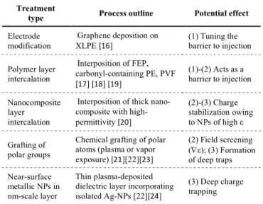
Table 1 provides a non-exhaustive overview of the methods that have been tested to modify interfaces.
Table 1. Principle of the different interface-modification methods addressed for controlling charge injection.
Treatment
type Process outline Potential effect
Electrode modification
Graphene deposition on
XLPE [16] (1) Tuning the barrier to injection Polymer layer intercalation Interposition of FEP, carbonyl-containing PE, PVF [17] [18] [19] (1)-(2) Acts as a barrier to injection Nanocomposite layer intercalation
Interposition of thick nano-composite with high-permittivity [20] (2)-(3) Charge stabilization owing to NPs of high ε Grafting of polar groups
Chemical grafting of polar atoms (plasma or vapor exposure) [21][22][23] (2) Field screening (Ñε); (3) Formation of deep traps Near-surface metallic NPs in nm-scale layer Thin plasma-deposited dielectric layer incorporating isolated Ag-NPs [22][24]
(3) Deep charge trapping
C. Electrode modification
As stated previously, it is well known that modifying the nature of the electrodes has a substantial impact on charge build-up; it is for example clear when changing electrodes in PEA set-up. Lei et al [16] reported on the use of graphene-containing electrodes on charge injection into XLPE.
Coating of samples with a few-layer graphene was achieved after dissolution in an appropriate solvent. Injection of negative charges was reduced (compared to Al electrode) when one-side of film was covered with graphene. The difficulty with playing with electrode material work function is that increasing the barrier to one polarity charges should increase that for the opposite polarity: the dominant carrier should be identified for a particular material. This holds if all parameters are same elsewhere, meaning no modification of surface chemistry and profile because of the deposition process. Besides, the trends do not necessarily follow the expected behavior considering the metal work function [3].
D. Layer intercalation
Different layers were used as injection blocking: for example Tanaka et al [17] used LDPE with grafted carbonyl groups as blocking layers. Fluorinated polymers, being FEP [18] or PVF [19] were also efficient in preventing both hole and electron injection. The works were achieved mainly for discriminating injection from internal generation of charges into LDPE and not much discussion about the blocking effect was given. The increase in barrier to injection as well as deep charge trapping (fluorinated polymer are much used as electrets) can be the contributing processes to the injection
Fig. 2 Scheme of trap-aided charge injection in a dielectric and different ways the charge injection can be controlled. (1): barrier to injection; (2): transport through localized states; (3): introduction of deep levels.
1
2 3
mitigation. More recently Li et al [20] investigated the effects of inserting ≈30 µm thick nanocomposite layers near the electrodes. Nanocomposites were made of high permittivity nanoparticles as TiO2 dispersed in a LDPE matrix same as
bulk LDPE layer. The nanocomposites taken alone indicated relatively space charge free behavior compared to pure LDPE. When associating such layers, mostly interface charges were seen due to the mismatch in permittivity and conductivity. As the conductivity in the nanocomposites was substantially lower than in LDPE, interface charges appeared as heterocharges relatively to the adjacent electrode: the field at the electrode was enhanced which might go against the expected trend.
E. Polymer modification
Instead of intercalating a layer which represents an extra interface in the dielectric, it is tempting to chemically modify the surface to tune the interface properties. Modification can be achieved by plasma attack, which represents rather mild effects. In recent years most of the attempts in this way were achieved with exposing the surface to fluorine vapors, which is a well-known process to modify adhesion properties. Material can be modified over depths of the order of 1 µm. The presence of traces of oxygen would have a negative effect on treatment efficiency. According to An et al [21], the key point in charge injection mitigation is the reduction in free volume in the surface layer, before increased surface layer permittivity or deep charge traps formation. In a recent study we observed that fluorination or oxyfluorination treatments were less efficient in blocking hole injection than electron injection, presumably because the interface tailoring shallows hole traps [22].
Fluorination maybe used to modify the behavior of interface charge characteristics in dielectric/dielectric interfaces as in LDPE/EPDM joints [23]. The charge release rate could be improved as well as amount of charges, due to change in trap distributions in both materials.
F. Artificial traps formation
Another strategy worth mentioning is the formation of a nanocomposite film with Ag nanoparticles embedded in organosilicon plasma layer, the Ag-NPs being settled at a controlled distance from the interface [24]. Very efficient charge injection mitigation for both electrons and holes was observed with this process and the apparent conductivity was substantially reduced. Here the effects were ascribed to the capture of injected charges by the Ag-NPs and the interface field screening it induces.
III. CHARGE SUPPRESSION AT GAS/SOLID INTERFACE
A. Charge origins
The pioneering research in gas/solid interface charging phenomena of insulators dates back to 1982 when Cooke found that the insulator surface accumulates charges when the surface charge arrival rate exceeds the surface charge conduction rate [25]. It has been widely accepted that the surface charge accumulation of insulators either arises from the conduction current from the volume/surface, and/or it can be due to charges migrating along the direction of electric field lines in the gas phase. Recently it was verified that surface charge is dominated by different charge sources due to the difference of local electric field, as shown in Fig. 3 [26].
Accordingly, when dealing with methods to suppress the surface charge accumulation, it is very important to firstly clarify the dominant charge characteristics and the way these charges influence surface flashover behaviors under specific insulation-electrode arrangement. Keeping this in mind can we further consider suitable charge tailoring methods targeting the decay of these charges. Table 2 provides a non-exhaustive overview of the methods that have been studied to suppress surface charge accumulation.
Table 2. Principle of methods to suppress charge accumulation from different origins. ISCD-increasing surface charge decay; SCV-suppressing charge from volume; MLEF-modification of local electric field; ICC-initiatively charge control method.
Cate-gory Treatment type Techniques Potential effect
ISCD Fluorination [27] [28] Direct fluorination Increasing surface charge decay rate by
increasing surface conductivity/ introducing shallow traps DBD Plasma [29] Etching; deposition Coatings [30][31] SiO2/Epoxy coating; TiO2/Epoxy coating Other [32][33][34] Gamma rays; ozone treatment; MFF filler SCV Nano surface
coatings [35] Cr2O3 coating Suppressing charge injection/transport by introducing deep traps/thermal barrier effect Bulk doping [36][37][38] K2Ti6O13 Whisker; C60 particle MLEF Nonlinear conductivity [39][40] [41][42] Nonlinear particles; Non-linear coatings
Optimizing the local electric field and improving surface charge dissipation ICCM Charge adaptively controlling spacer[43] Modifying spacer shape and doping with nonlinear materials Controlling charge location and decaying charge initiatively
B. Improving surface charge decay
A more conductive surface has a higher surface charge
decay rate. Fluorination, plasma treatment, surface coatings, gamma ray irradiation, and ozone treatment, etc., have verified capability to increase the surface conductivity and decay surface charges.
Fluorination can be a useful tool to increase surface conductivity of epoxy resin and the increase of surface conductivity can reach up to 2-3 orders of magnitude compared with the pure epoxy. An et al. concluded that temperature and time during fluorination are two important factors controlling the fluorination process and affecting the surface conductivity, while the effect of temperature on the surface conductivity is more significant than that of the fluorination time duration [27]. However, it is interestingly to note that some researchers argued that the increase in the surface conductivity may not be due to the fluorine layer itself, but because of the moisture absorbed in the surface layer [28]. T. Shao et al. found that the plasma treatment increases surface conductivity of epoxy surface, which promotes surface charge decay rate [29]. Meanwhile, shallow traps introduced by nano-TiO2 [30], SiOx [31] surface
coatings were studied to suppress charge accumulation. Surface conductivity can be increased also by gamma rays [32], surface roughness treatment [33], as well as ozone treatment [34], which have been extensively discussed by researchers.
C. Suppressing volume charge injection
Different to the way to accelerate charge decay rate as discussed in Section B, to suppress charge injection refers to limit the charges originated from volume conduction current. A further difficulty in the exercise of controlling surface potential in spacers is the fact that the potential built may result from charges stored in the bulk of the insulation and not only on the surface. Therefore, both coating and doping the bulk insulation have been considered. The problem can be solved at the source, i.e. by limiting injection from the insulation into the dielectric, as addressed in section II, or by limiting transport into the volume of the dielectric.
A dense, ordered Cr2O3 nano-coating created by the
magnetron sputtering method on the epoxy surface has been verified as an effective way to restrain charge injection from the HV negative electrode into the surface coating since large amount of deep traps can be introduced [35]. Bulk conductivity can be decreased by dispersing surface-modified silica nano-particles [36] as well as Buckminster-fullerene C60 [37] into epoxy. Apart from that, He et al. focus on the
restrain of charge transport inside the volume at high temperature, by doping K2Ti6O13 whiskers into epoxy [38].
They took advantage of the thermal barrier effect of K2Ti6O13
whiskers to suppress the transport of homo-polar charges in the bulk, and the results demonstrate that the restrain of heat propagation due to the thermal barrier property of K2Ti6O13
suppresses charge transport effectively under high temperature.
D. Local electric field modification
Nonlinear conductivity composites behave nonlinear effect with respect to the increasing of electric field. Such composite is filled with inorganic fillers such as ZnO, SiC, etc. to have the nonlinear property. Tenzer et al. proposed an insulator using oriented “MFF (Minatec® functional filler)” filler [39] and a more uniform electric field distribution under the effect of room temperature and temperature gradient was obtained compared with that of the traditional spacer. Du and Xue studied effect of SiC particles doped coatings on surface charge decay and surface flashover voltage [40, 41] based on dipping and spraying, respectively. They both found that a suitable nonlinear coating suppresses surface charge and results in higher surface flashover voltage. Interestingly, our
work showed a decreasing trend in surface flashover voltage with SiC being doped both into the cone type insulator and the post type insulator [42].
E. Initiatively charge control
A novel design of HVDC spacer was introduced based on the concept of adaptively controlling surface charges using nonlinear materials. This method, unlike commonly used traditional approaches, proposed a novel idea of controlling the location of accumulated charges and then properly decaying of these charges taking advantage of the electric field distortion due to charge accumulation, which fundamentally solves the problem of surface charge accumulation. The electrical and mechanical test results show that the charge adaptively controlling spacer has high operating capability under DC voltage and has great industrial application potential [43].
IV. DISCUSSION AND OUTLOOKS
Of all the charge tailoring techniques mentioned targeting on preventing charge generation or forcing the decay of charges for mitigating either injection or gas-solid interface charging, resistivity (shallow traps) and deep trapping are parameters that researchers most concerned. The tailoring that is achieved with the introduction of novel trapping levels must present an interplay with the existing material, providing the right compatibility in terms of energy levels as well as respecting process compatibility.
There exist several solutions for limiting charge injection at electrode dielectric interfaces. Questions to consider are how far the applied solution works for both positive and negative carriers, and may the process have counter-productive effects by preventing charge extraction at opposite interface, forming hetero-polar charge build-up: hence the need to think in terms of global design for the system. Another aspect not really addressed here is how far the process can be transferred at the scale of cable extrusion process for example and how far it may interfere with the extra-clean conditions necessary to reach high reliability in high voltage products.
In the case of surface charging specifically, it should be emphasized that before choosing charge tailoring methods, one should firstly clarify the charge origin we were to deal with, i.e. the homo-polarity charge due to injection or the hetero-polarity charge from the gas phase. Under this premise are we able to regulate the charge in a targeted manner. However, during changing of surface conductivity and traps, etc., the surface morphology, which has been verified to be an important parameter affecting surface flashover voltage, is usually changed. This makes it difficult for us to discern what parameter change plays a decisive role in surface charge decay and surface flashover voltage increase. For example, in the fluorination process, is it the topology, the morphology changing or the conductivity increase that contributes more to the surface flashover voltage increase? When changing an electrode material, is it the energy level of the metal that matters or the change in surface states produced by the change in deposition process? In addition, results obtained by different researchers showed optimal conductivity values which differs by several orders of magnitudes, which make it difficult to compare with each other’s results and find the optimal margin regarding determining a suitable surface conductivity ready for industry application.
REFERENCES
[1] D. Fabiani et al., "Guest editorial: Interface charging phenomena for dielectric materials review papers," IET High Volt., vol. 5, pp. 93-94, 2020.
[2] G. Chen, Y. Tanaka, T. Takada, and L. Zhong, "Effect of polyethylene interface on space charge formation," IEEE Trans. Dielectr. Electr. Insul., vol. 11, pp. 113-121, 2004.
[3] M. Taleb, G. Teyssèdre, and S. Le Roy, "Role of the interface on charge build-up in a low-density polyethylene: surface roughness and nature of the electrode," Proc. IEEE Conf. Electr. Insul. Dielectr. Phenom. (CEIDP), pp. 112-115, 2009.
[4] T.S. Sudarshan, and R.A. Dougal, "Mechanisms of surface flashover along solid dielectrics in compressed gases: a review," IEEE Trans. Electr. Insul. , vol. EI-21, pp. 727-746, 1986.
[5] C. Li, J. Hu, C. Lin, and J. He, "The potentially neglected culprit of DC surface flashover: electron migration under temperature gradients," Sci. Rep., vol. 7, pp. 1-11, 2017.
[6] C. Li, et al., "Charge cluster triggers unpredictable insulation surface flashover,", submitted to J. Phys. D: Appl. Phys., 2020.
[7] M. Tschentscher, and C. M. Franck, "Microscopic charge provision at interfaces of gas-insulated (HVDC/HVAC) systems," IEEE Trans. Dielectr. Electr. Insul., vol. 25, pp. 1177-1185, 2018.
[8] G. Chen, Y. Tu, S. Wu, et al., "Intrinsic hetero-polar surface charge phenomenon in environmental friendly C3F7CN/CO2 gas mixture," J.Phys. D: Appl. Phys., vol. 53, p. 18LT03, 2020.
[9] P. Morshuis, "Interfaces: To be avoided or to be treasured? What do we think we know? ," Proc. 2013 IEEE Internat. Conf. Solid Dielectrics (ICSD), pp. 1-9, 2013.
[10] T. Takada, Y. Hayase, Y. Tanaka, and T. Okamoto, "Space charge trapping in electrical potential well caused by permanent and induced dipoles for LDPE/MgO nanocomposite," IEEE Trans. Dielectr. Electr. Insul., vol. 15, pp. 152–160, 2008.
[11] F. Nilsson, M. Karlsson, L. Pallon, M. Giacinti, R.T. Olsson, D. Venturi, U.W. Gedde, and M.S. Hedenqvist, "Influence of water uptake on the electrical DC-conductivity of insulating LDPE/MgO nanocomposites," Composites Sci. Technol., vol. 152, pp. 11-19, 2017. [12] G. Chen, J. Zhao, S. Li and L. Zhong, "Origin of thickness dependent dc electrical breakdown in dielectrics," Appl. Phys. Lett., vol. 100, p. 222904, 2012.
[13] D. Min, S. Li and Y. Ohki, "Numerical simulation on molecular displacement and DC breakdown of LDPE," IEEE Trans. Dielectr. Elect. Insul., vol. 23, pp. 507-516, 2016.
[14] M. Taleb, G. Teyssèdre, S. Le Roy, and C. Laurent, "Modelling of charge injection and extraction in a metal/polymer interface through an exponential distribution of surface states," IEEE Trans. Dielectr. Electr. Insul., vol. 20, pp. 311-320, 2013.
[15] S.Y. Jung, C.H. Kim, Y. Bonnassieux, and G. Horowitz, "Injection barrier at metal/organic semiconductor junctions with a Gaussian density-of-states," J. Phys. D: Appl. Phys., vol. 48, n° 395103, 2015. [16] Z. Lei, D. Fabiani, C. Li, S. V. Suraci, G. Selleri, T. Han, M. Speranza,
F. Grolli, and F. Palmieri, "Effect of graphene coating on space charge characteristic of XLPE and semiconductive layer at different temperatures," IEEE Access, vol. 7, pp. 124540-124547, 2019. [17] Y. Tanaka, Y. Li, T. Takada and M. Ikeda, "Space charge distribution
in low-density polyethylene with charge-injection suppression layers," J. Phys. D: Appl. Phys., vol. 28, pp. 1232-1238, 1995.
[18] T. Hori, K. Kaneko, T. Mizutani and M. Ishioka, "Space charge distribution in low-density polyethylene with blocking layer," IEEE Conf. Electr. Insul. Dielectr. Phenom. (CEIDP), pp.197–200, 2003. [19] J. Xia, Y. Zhang, Z. An and F. Zheng, "Blocking effect of PVF on space
charge injection into low density polyethylene," Proc. Int'l. Conf. on Solid Dielectrics (ICSD, Potsdam, Germany), pp. 379–382, 2010. [20] S.T. Li, N. Zhao, Y.J. Nie, X. Wang, G. Chen, and G. Teyssedre,
"Space charge characteristics of LDPE nanocomposite/LDPE insulation system," IEEE Trans. Dielectr. Electr. Insul., vol. 22, pp. 92-100, 2015.
[21] Z. An, C. Liu, X. Chen, F. Zheng, and Y. Zhang, "Correlation between space charge accumulation in polyethylene and its fluorinated surface layer characteristics," J. Phys. D: Appl. Phys., vol. 45, n° 035302, 2012. [22] G. Teyssedre, S.T. Li, K. Makasheva, N. Zhao, L. Milliere, and C. Laurent," Interface tailoring for charge injection control in polyethylene," IEEE Trans. Dielectr. Electr. Insul., vol. 24, pp. 1319-1330, 2017.
[23] J. Li, B.X. Du, J.G. Su, H.C. Liang, and Y. Liu, "Surface layer fluorination-modulated space charge behaviors in HVDC cable accessory," Polymers, vol. 10, n° 500, 2018.
[24] L. Milliere, K. Makasheva, C. Laurent, B. Despax, L. Boudou, and G. Teyssedre, "Silver nanoparticles as a key feature of a plasma polymer composite layer in mitigation of charge injection into polyethylene under DC stress,'' J. Phys. D: Appl. Phys., vol. 49, n° 015304, 2015. [25] C.M. Cooke "Charging of insulator surfaces by ionization and transport
in gases," IEEE Trans. Electr. Insul., vol. EI-17, pp.172-178, 1982. [26] C. Li, C. Lin, G. Chen, Y. Tu, Y. Zhou, Q. Li, B. Zhang, and J. He,
"Field-dependent charging phenomenon of HVDC spacers based on dominant charge behaviors," Appl. Phys. Lett., vol. 114, p. 202904, 2019. [27] Z. An, Q. Yin, Y. Liu, F. Zheng, Q. Lei, and Y. Zhang, "Modulation of
surface electrical properties of epoxy resin insulator by changing fluorination temperature and time," IEEE Trans. Dielectr. Electr. Insul., vol. 22, pp. 526-534, 2015.
[28] A. Mohamad, G. Chen, Y. Zhang, and Z. An, "Moisture effect on surface fluorinated epoxy resin for high-voltage DC applications," IEEE Trans. Dielectr. Electr. Insul., vol. 23, pp. 1148-1155, 2016. [29] T. Shao, F. Liu, B. Hai, Y. Ma, R. Wang, and C. Ren, "Surface
modification of epoxy using an atmospheric pressure dielectric barrier discharge to accelerate surface charge dissipation," IEEE Trans. Dielectr. Electr. Insul., vol. 24, pp. 1557-1165, 2017.
[30] Y. Tu, F. Zhou, Y. Cheng, H. Jiang, C. Wang, F. Bai, and J. Lin, "The control mechanism of micron and nano SiO2/epoxy composite coating on surface charge in epoxy resin," IEEE Trans. Dielectr. Electr. Insul., vol. 25, pp. 1275-1284, 2018.
[31] R. Wang, H. Lin, Y. Gao, C. Ren, K. Ostrikov, and T. Shao, "Inorganic nanofilms for surface charge control on polymer surfaces by atmospheric-pressure plasma deposition," J. Appl. Phys., vol. 122, p. 233302, 2017.
[32] B. Du and Y. Gao, "Dynamic behavior of surface charge on gamma-ray irradiated polybutylene naphthalate," Polym. Degrad. Stabil., vol. 94, pp. 139-143, 2009.
[33] K. Nakanishi, A. Yoshioka, Y. Arahata, and Y. Shibuya, "Surface charging on epoxy spacer at DC stress in compressed SF6 gas," IEEE Trans. Power Ap. Syst., vol. PAS-102, pp. 3919-3927, 1983. [34] Y. Huang, D. Min, D. Xie, S. Li, X.Wang, and S.Lin, "Surface
flashover performance of epoxy resin microcomposites infulenced by ozone treatment," Proc. 2017 IEEE Int. Symp. Electr. Insul. Materials (ISEIM), pp. 235-238, 2017.
[35] C. Li, J. Hu, C. Lin, and J. He, "The control mechanism of surface traps on surface charge behavior in alumina-filled epoxy composites," J.Phys. D: Appl. Phys., vol. 49, p. 445304, 2016.
[36] P. Chu, H. Zhang, J. Zhao, F. Gao, Y. Guo, B. Dang, and Z. Zhang, "On the volume resistivity of silica nanoparticle filled epoxy with different surface modifications, " Compos. Part A, vol.99, pp.139-148, 2017. [37] B. Zhang, W. Gao, Y. Hou, and G. Zhang, "Surface charge
accumulation and suppression on fullerene-filled epoxy-resin insulator under DC voltage, " IEEE Trans. Dielectr. Electr. Insul., vol. 25 pp. 2011-2019, 2018.
[38] S. He, C. Lin, J. Hu, C. Li, and J. He, "Tailoring charge transport in epoxy based composite under temperature gradient using K2Ti6O13 and asbestine whiskers," J.Phys. D: Appl. Phys., vol. 51, p. 215306, 2018. [39] A.Winter, et al., "Compact gas-solid insulating systems for high-field-stress in HVDC applications, ". In: CIGRE Study Committee B3 & Study Committee D1 Colloquium, 2013.
[40] H. Liang, B. Du, J. Li, Z. Li, and A. Li, "Effects of non-linear conductivity on charge trapping and de-trapping behaviours in epoxy/SiC composites under DC stress, " IET Sci. Meas. Technol., vol. 12, pp. 83-89, 2018.
[41] J. Xue, Y. Li, J. Dong, J. Chen, W. Li, J. Deng, and G. Zhang, "Surface charge transport behavior and flashover mechanism on alumina/epoxy spacers coated by SiC/epoxy composites with varied SiC particle size," J.Phys. D: Appl. Phys., vol. 53, p. 155503, 2020.
[42] S. He, C. Li, C. Lin, J. Hu, J. He, and Z. Sun, "Potential feasibility analysis and validation of application of non-linear materials in charge regulation of gas-solid interface," Proceedings of the CSU-EPSA, DOI:10.19635/j.cnki.csu-epsa.000343. (in Chinese)
[43] C. Li, C. Lin, J. Hu, W. Liu, Q. Li, B. Zhang, S. He, Y. Yang, F. Liu, and J. He, "Novel HVDC Spacers by adaptively controlling surface charges – Part I: Charge transport and control strategy," IEEE Trans. Dielectr. Electr. Insul., vol. 25, pp. 1238-1247, 2018.
![Fig. 1 Scenarios for charging phenomena and surface charge triggered flashover for HVDC spacer due to AIR expansion [5] as well as charge cluster evolution [6]](https://thumb-eu.123doks.com/thumbv2/123doknet/14374235.504843/2.892.472.816.839.1069/scenarios-charging-phenomena-surface-triggered-flashover-expansion-evolution.webp)
![Fig. 3 Field dependence model of dominant charge behavior. [26]](https://thumb-eu.123doks.com/thumbv2/123doknet/14374235.504843/4.892.463.827.562.1010/fig-field-dependence-model-dominant-charge-behavior.webp)
