HAL Id: tel-01123983
https://tel.archives-ouvertes.fr/tel-01123983
Submitted on 5 Mar 2015HAL is a multi-disciplinary open access
archive for the deposit and dissemination of sci-entific research documents, whether they are pub-lished or not. The documents may come from teaching and research institutions in France or abroad, or from public or private research centers.
L’archive ouverte pluridisciplinaire HAL, est destinée au dépôt et à la diffusion de documents scientifiques de niveau recherche, publiés ou non, émanant des établissements d’enseignement et de recherche français ou étrangers, des laboratoires publics ou privés.
TH `
ESE
Pour obtenir le grade de
DOCTEUR DE L’UNIVERSIT ´
E DE GRENOBLE
Sp ´ecialit ´e : Physique Arr ˆet ´e minist ´erial :
Pr ´esent ´ee par
Piotr Laczkowski
Th `ese dirig ´ee parDr. Alain Marty
et codirig ´ee parDr. Laurent Vila
pr ´epar ´ee au sein du Laboratoire Nanostructure et Magn ´etisme
et del‘ ´ecole doctorale de Physique
Spin currents and spin Hall effect
in lateral nano-structures
Th `ese soutenue publiquement le , devant le jury compos ´e de :
Prof. Alain Schuhl
Institut N ´eel, CNRS Grenoble, Pr ´esident
Prof. Albert Fert
Unit ´e Mixte de Physique CNRS/Thales (UMR137), Examinateur
Prof. Francois Montaigne
Laboratoire de Physique des Mat ´eriaux, Institut Jean Lamour, Nancy, Rapporteur
Dr. Michel Viret
Service de Physique de l’Etat Condens ´e, CEA Orme des Merisiers, Rapporteur
Dr. Alain Marty
INAC/SP2M/NM, CEA Grenoble, Directeur de th `ese
Dr. Laurent Vila
“Learn from yesterday, live for today,
hope for tomorrow. The important thing is
to not stop questioning.”
Acknowledgements
I would like to express my gratitude to all the wonderful people that I had pleasure to meet during this 3-year adventure ! Thank you very much for your help and guidance - I wish you all the best and hope one day our paths will cross again !!
Laurent: It is your patience, knowledge and trust in me that resulted in this wonderful cooperation and in such an extraordinary adventure. I wanted to thank you for being there for me as my supervisor but mostly as a friend in every aspect of day-to-day life and of course for all the precious knowledge ! You are the best supervisor that one can imagine !
Jean-Philippe: Thank you for sharing with me your wonderful academic and scientific point of view based upon simplicity, uniformity (not only colors, types etc..) and clarity ! For keeping an eye on me whenever I was meant to turn in a wrong direction (especially during the ski season ;) and for all the exciting out-off adventures (I will never forget about it) !
Alain: Thank you for your guidance and knowledge, for sharing with me whatever is the best in science ! Thanks for early morning discussions and for sharing my passion for programming and the open source software !! I will always admire your knowledge (“you are the man”) !
Cyril and Lucien: Without you this work would be simply impossible, so let me thank you for all your hard work, perfect organization and precision always coming along with a very good atmosphere, humor and music (keep on rocking) !!!
Dai: Thank you for this wonderful time spent together as office-mates and after-all as friends during this PhD journey ! I wish you the very best in every aspect and hope that one day we could work together once again!
Irina: Thanks for your help and guidance, for your soft heart and good example ;) . I will always remember the football tournaments, captain !
Carlos, Williams and Murat: Thanks for completing this great team, for motivation, humor and all of many adventures ! Have to say it was a great experience to work with you !
Thilbaut, Jean-Luc, Helge, Christophe, Sebastien, Gile, Tristan, Milène, Perrine and all of the clean room staff members in PTA and CIME: Thank you very much for making me one of you as a clean room/white-ninja family member - It was a great experience / wonderful memories !!!
Table of Contents
Introduction 1
Outline 5
1 Theory of spin transport in lateral spin-valves 7
1.1 Basics of spin transport in metals . . . 7
1.1.1 Transport in a ferromagnetic metal . . . 8
1.1.2 Electron spin transport in a metal . . . 9
1.1.2.1 The spin-flip mechanism . . . 11
1.2 Ferromagnetic/Non-magnetic interface . . . 11
1.3 Spin current detection . . . 13
1.3.1 GMR and the electro-chemical landscape . . . 13
1.3.2 Pure spin current injection and detection . . . 15
2 Optimization of the spin signal 21 2.1 Introduction . . . 21
2.2 Geometry optimization . . . 22
2.3 Multi-level and multi-angle method . . . 23
2.3.1 Multi-level method . . . 25
2.3.2 Multi-angle method . . . 26
2.3.2.1 Standard shadow method . . . 26
2.3.2.2 Multi-angle shadow method . . . 27
2.4 Materials dependence. . . 29
2.4.1 Spin signal for different materials . . . 29
2.4.2 Permalloy ferro-magnetic electrodes . . . 34
2.5 Conclusions . . . 37
3 Characterization of the spin dependent transport properties in lateral spin-valves 39 3.1 Basic characterization techniques . . . 39
3.1.1 Cross-shaped devices for resistivity measurements . . . 40
3.1.2 Atomic Force Microscope measurements . . . 41
3.5 Conclusions . . . 56
4 Lateral confinement effect 59 4.1 Samples and measurements . . . 59
4.2 Results and theory/simulation comparison . . . 63
4.2.1 Simulations of the lateral confinement . . . 67
4.3 Conclusions . . . 69
5 Signal enhancement and spin precession in LSV with tunnel barriers 71 5.1 Samples and measurements . . . 71
5.2 Spin signal amplification . . . 72
5.3 The Hanle effect . . . 73
5.3.1 Magnetic characterization . . . 75
5.3.2 Analysis methods . . . 75
5.3.3 Spin signals comparison . . . 77
5.4 Conclusions . . . 78
6 Spin Hall Effect 79 6.1 Spin Hall Effect . . . 79
6.2 Application . . . 81
6.3 New materials. . . 82
6.3.1 Spin pumping experiments . . . 86
6.4 Spin diffusion length measurements . . . 88
6.4.1 Methods and devices . . . 89
6.4.2 Spin diffusion length evaluation for Pt and AuW . . . 90
6.5 Spin Hall effect measurements . . . 94
6.5.1 Methods . . . 95
6.5.2 Results for Pt and AuW . . . 97
6.5.3 Shunting effect . . . 100
TABLE OF CONTENTS
A Simulations by Finite Element Method 107
A.1 Methods . . . 107
B Nano-fabrication methods 111 B.1 Procedures and equipment . . . 111
B.1.1 Electron-beam lithography . . . 111
B.1.2 Resist revelation . . . 113
B.1.3 Metal evaporation . . . 114
B.1.3.1 Ion-milling . . . 114
B.1.3.2 The hard mask approach . . . 114
B.1.4 Lift-off process . . . 115
B.1.5 Recipes . . . 115
C Spin Pumping methods 117 C.1 Methods . . . 117
Introduction
In conventional electronics, information is stored, manipulated and transported by electron charges. Further progress can no longer be accomplished by merely scaling transistors to smaller geometries, mainly because of the dramatic increase in power consumption in highly scaled Com-plementary Metal Oxide Semiconductor (CMOS) devices. Advances in new magnetic materials and devices, based on the electronic spin, build an attractive alternative to maintain the progress in computation and data storage [1].
As it becomes clear that breakthroughs are needed, nano-magnetic systems could provide unique opportunities. Indeed, the dissipation energy of magnetic processes can be orders of magnitude smaller than those of CMOS. Furthermore, most magnetic applications are inher-ently non-volatile and radiation hard, and could lead to increased data processing speeds [2]. Spin-based memories and logic devices could complement or supplant traditional semiconductor microelectronics, especially since spintronics nowadays involves not only metals [3] but semicon-ductors [4] or even graphene-based structures [5].
In 1988 Albert Fert and Peter Grünberg discovered independently the Giant Magneto-Resistance effect (GMR) [6, 7]. A GMR device consists basically of a trilayer vertical structure, with two ferro-magnetic layers separated by a thin non-magnetic metallic material [8]. The first observa-tion of GMR in a spin-valve [9], in which the magnetization of the free layer can be reversed by small magnetic fields, and the discovery of Tunnel Magnet-Resistance (TMR) [10, 11, 12], led to the miniaturization of the hard drives recording heads, and thus to a strong increase of the storage density [1].
As GMR implies spin injection from a ferromagnetic into a non-magnetic metal, its discovery, showed the importance of spin accumulation and of spin-polarized currents [13,14]. The devel-opment of the TMR, with ratios up to almost 605% at room temperatures [15] and 1144% at 5 K [16], provided the basis for application of this effect in random magnetic access memory devices (MRAM). Also, intensive theoretical studies on the spin injection from a magnetic metal into a non-magnetic semiconductor, brought to light the conductivity mismatch problem, resolved by the introduction of a thin isolating layer in between the two materials [17].
Both GMR and TMR effects thus allow an efficient detection of the magnetically encoded informations. The next important stage, for spintronics, was the ability not only to read infor-mation, but to write it using spin currents. The concept of spin angular momentum transfer, associated to the flow of a spin-polarized current into a ferromagnet, has been introduced in 1996.
pumping (ferro-magnetic resonance) [26].
In this context, the Spin Hall Effect (SHE) recently gained the interest of theoreticians and experimentalists, since it provides an alternative spin current source or spin current detector, that does not require magnetic materials nor magnetic fields [27, 28]. The spin accumulation is generated by the charge current passing through the material via the spin-orbit interactions [24]. In this case, the longitudinal charge current is transformed into a transverse spin current. The SHE is quantified by the ratio of the conversion of charge to spin current, called the spin Hall angle (SHA). One could imagine many possible applications of the SHE, if the ratio of conversion could be comparable to what can be obtained by magnetic materials in spin-valves or tunnel junctions.
Among the variety of possible applications of this effect, some have been already explored during the time of this thesis. The spin-torque switching of ferro-magnets, using SHE induced spin currents was recently demonstrated experimentally for tantalum [29], event at room temper-ature. Moreover, experiment on the spin-torque ferromagnetic resonance, induced by the SHE, was also reported [30]. There were also propositions of the spin Hall effect transistors, allowing detection directly along the gated semiconductor channel [31].
In the SHE, the same spin accumulation is generated everywhere at the surface of the material. One can thus imagine a spin current generation line, with multi terminals connection to it. At each terminal the same amount of the spin current would be generated, independently on the terminals number. This could be used, for example, in a massive depinning of the domains walls by exerted spin-torque. Nevertheless, as the SHE deals with spin current and do not induce voltage drop in a material, new experimental techniques and schemes are required.
The SHE-induced spin accumulation in semiconductors has drawn much attention because of its compatibility with the conventional CMOS technology. Up to now, semiconductors such as GaAs, ZnSe have exhibited a very small SHE and no electrical detection has been reported. In contrast, metals, such as Pt or Ta, have been successfully used to detect the SHE, even at room temperature, exhibiting the largest spin Hall angle (> 10−2), reported so far for pure materials [32,33]. Large spin Hall angles, reaching 0.025 (2.5% of conversion), were found many years ago for materials doped with non-magnetic impurities, what was demonstrated by Fert et al. [34] for
INTRODUCTION
Cu doped with Ir, Ta and Lu. Also, very recent experiments showed large SHA, of the order of 2% for Cu doped with Ir impurities [35]. The quantitative estimation of the spin Hall angle is actually under intensive debate, and the experimental procedure has still to be carefully defined. At the beginning of this thesis, the highest spin Hall angle was reported for Pt, with a value smaller than 10−2.
Electrical detection has been shown for metals, even with reversible conversion of spin to charge current, reflecting the inverse and direct spin Hall effects. These measurements were made using either tunneling [36] or ohmic contacts [32,33,37] in lateral spin-valve (LSV) devices or spin-pumping technique [38, 39,40,41]. The spin pumping and the LSVs with ohmic contacts, where the SHE material was integrated, are the two complementary techniques, allowing good characterization of new SHE materials.
The spin pumping can now give access to the quantitative determination of the SHE [26,42]. The ferromagnetic resonance is used to induce oscillations of the magnetization in the ferro-magnet, deposited on the non-magnetic layer. These oscillations pump spins into the non-magnetic material, thus creating a vertical spin current detectable via the inverse SHE [43]. The spin diffusion length, necessary for SHA estimation, can be only evaluated by studying of the thickness variation of the SHE material. However, that requires several samples preparation, and becomes difficult for materials with short spin diffusion length, as it would require fabrication of the ultra-thin layers [44]. Complementary techniques are thus required.
The electrical SHE experiments are based on lateral spin-valves, which consist of two ferro-magnetic electrodes linked by the non-ferro-magnetic channel. In these devices, the material with strong spin-orbit interaction is inserted between the two ferro-magnetic electrodes. Most of the work done on spin transport has focused on the vertical [8], with much less effort concentrated on the lateral spin-valve structure. The development of this aspect is equivalently important, since many future spintronics components will require lateral integration [45]. Moreover, the LSVs allow for the spatial separation of the charge and spin currents [46,47], thus providing a powerful tool for detecting spin-related phenomena without the Anisotropic Magneto-Resistance (AMR) nor the Hall effect contributions to the output signal [48]. The additional advantage of the lateral structures comes from the possibility of applications in multi-terminal geometries, like a spin-flip transistor [49]. That is much more complicated in the case of the vertical devices.
The electrical spin injection in metallic LSVs was first demonstrated, in the non-local ge-ometry, by Johnson and Silsbee [47] for permalloy ferro-electrodes deposited on top of a bulk aluminum. The real interest however, flourished after the work of Jedema et al. [50] on the nano-scale LSVs, patterned by electron beam lithography, resulting in the investigation of many different materials, using different geometries [51, 52, 53, 54, 36]. However, one has to resolve technical issues such as efficient injection, transport, control, and detection of spin polarization as well as spin-polarized currents.
In the frame of this PhD thesis, the main challenge consists of the development of efficient characterization means of the SHE and its application to the characteriza-tion of dilute alloys. New materials are forecasted to target enhanced spin-orbit interaccharacteriza-tion,
OUTLINE
Outline
This PhD manuscript is divided into six chapters, organized in the following order:
Chapter1Description of the basic transport theory in lateral spin vales, necessary for understanding the work presented in the manuscript. The GMR and Non-Local injection and detection concepts are introduced and explained in the framework of the electro-chemical potential distribution.
Chapter 2 Optimization of the spin signal in LSV, aiming at highly efficient spin injection and reliable spin detection, is presented. The description is based upon the 1D spin transport model and underlines the importance of the interface, ge-ometry and nano-fabrication methods. All these aspects are discussed in details, and the optimization procedures are presented.
Chapter 3 Description of the basic methods and their application for spin dependent transport characterization in the lateral nano-structures is presented. Material pa-rameters are extracted using 1D standard model and the Finite Element Method (FEM) approach. Also an alternative analysis based on the transfer matrix ap-proach is made. The evaluation of the parameters is also combined with FEM simulations providing a powerful tool for these analyses.
Chapter 4Further optimization of the LSV by confining laterally the spin accumula-tion into the useful, active part of the nano-structure is demonstrated. Analysis based on the transfer matrix theory, allowing complete description of the spin sig-nal amplification in the Py/Au nano-devices is presented, underlining the role of the spin current polarization and the spin current accumulation. The discussion of the amplification regimes for various geometries is given with the numerical calculations and FEM simulations.
Chapter 5 Vertical confinement of the spin accumulation by introduction of the tun-nel barriers between the ferro-magnetic and the non-magnetic material is demon-strated. This is done by inserting a natural oxide alumina barrier at the interface of the LSV. Spin precession is studied and characterized by the Hanle effect while applying the external magnetic field in and out of the samples plane.
Chapter6Description of the spin Hall effect is provided introducing basic ideas of the experimental detection methods. Methodology of the spin Hall angle evaluation is presented together with qualitative analyses for Pt and AuW based nano-devices, with both spin pumping and transport measurements.
Chapter 1
Theory of spin transport in lateral
spin-valves
The goal of this chapter is to introduce the basic physical concepts describing spin polarized trans-port in lateral nano-structures. First, parameters describing the general electronic transtrans-port in metals will be introduced, taking into account the spin degree of freedom. Also, a brief overview of the main spin-flip mechanisms in the non-magnetic metal will be presented. The spin diffusion model will be introduced and applied to the case of a single ferromagnetic/non-magnetic inter-face. This will be further extended to the case of a ferromagnetic/non-magnetic/ferromagnetic heterostructure with the concept of a ferromagnetic voltage probe. Finally, local (GMR) and non-local measurements will be presented and described in the lateral spin-valve with an empha-sis on the description of the electro-chemical landscape and the concept of pure spin currents.
1.1
Basics of spin transport in metals
In order to describe the spin transport, two important length-scales need to be taken into account. First of them is called the electron mean free path and is noted le. In lateral spin-valves,
one uses a diffusive transport regime which is applicable when le is shorter than the device dimensions (case of all nano-devices presented in this thesis). The second important length-scale is represented by the spin diffusion length (lsfN), which defines the material characteristic length over which the memory of the spin will be lost, its orientation randomized. In the following, the role of these quantities will be pointed out in the description of diffusive transport. In this picture the fully occupied states well below the Fermi surface are neglected.
For systems with two spin species, it is convenient to use a thermodynamic quantity called the electro-chemical potential (related to the chemical potential µchemthrough µ = µch−eV ,
where e is the absolute value of the electron charge and V is the electric potential). One can assign a separate electro-chemical potential associated to each spin specie, defined as the energy that has to be put into the system to increase by one the number of particles (containing the additional potential energy eV ).
Figure 1.1: The Stoner model of ferromagnetic transition metals, illustrated for the 3d shell. The spin states with the largest number of electrons are called majority spins, whereas those with the lower number are the minority spins. The Fermi energy level εF which separates the occupied
from unoccupied electron states is indicated by the dashed line. The centers of the majority and minority sub-bands are separated by the exchange splitting ∆exch. The quantization direction is determined by the −M direction and can be controlled by the external field H→ ext. [61]
two spin species can be treated separately. In a first approximation, spin-dependent transport can be described by two separated independent spin channels, following the model proposed by Mott [57]. This idea was followed by Fert and Campbell to describe the transport properties of Ni, Fe and Co based alloys [58] and further extended by Van Son et al. [59] to describe transport through transparent ferromagnetic/non-magnetic interfaces. The use of ferromagnets to inject and detect spins led to the discovery of the Giant Magneto-Resistance effect by the groups of Fert [6] and Grünberg [7]. That quickly led to the miniaturization of the recording heads of hard-disk drives, and earned Fert and Grünberg the 2007 Nobel Prize in Physics [8,60]. Valet and Fert [13] have developed Boltzmann equations based on the diffusion model including spin-flip scattering to analyze current perpendicular to the plane (CPP) GMR effect in magnetic multi-layers. This approach provides a full description of the spin transport in a lateral spin-valves.
1.1.1 Transport in a ferromagnetic metal
In a ferromagnetic material (F ) electrons strongly interact with each other via the exchange interaction. Even in the absence of a magnetic field this interaction creates a magnetic order responsible for a non-zero average magnetic momentum. In this manner, a collective degree of order of electrons spin creates a macroscopic magnetic moment e.g., magnetization.
The Stoner model, represented schematically in figure1.1, assumes that the density of states (DOS) for the majority and minority electrons is often nearly identical, but the states are shifted in energy with respect to each other by the exchange energy ∆exch. The quantization axis is given by the direction of the magnetization−M . Since the magnetization represents an average magnetic→ moment of a volume, and the magnetic moment of each electron is defined as m = −gµBs (where
1.1. BASICS OF SPIN TRANSPORT IN METALS
electron spin), the moment and the spin have opposite directions. Therefore, in the presented case, the majority states are spin-down and the minority states are spin-up [61]. The electrons responsible for electric transport in the transition metals (Ni, Fe, Co) are situated at the Fermi energy. The current is carried mainly by the s band electrons, whereas the s − d diffusion probability is responsible for the conductivity value. It mainly depends on the DOS at the d sub-bands since the probability of diffusion depends on available states at εF. Due to the energy splitting the DOS at the Fermi level is different for the two spin directions. This means that the total conductivity σ is determined by the conductivities of both spin-up electrons, σ↑, and
spin-down electrons, σ↓, being different. Note that in representation with respects to the
spin-transport, the majority and minority spin population are spin-up and spin-down respectively (contrary to the magnetic moment representation).
Treating independently each spin population, one can define the conductivities σ↑ and σ↓, in
a general case as follows:
σF↑ = αFσF; σF↓ = (1 − αF)σF (1.1)
where αF stands for the asymmetry of conduction in F (0 ≤ αF ≤ 1), and σF = σ↑+ σ↓.
In the bulk ferromagnet it is usually αbulkF > 0.5 (while considering the minority channel as one having lower conductivity and considering spin up as the majority), where the case of αF = 0.5 describes a non-magnetic metal.
We can use the two currents model to define the total current density, flowing in the ferromagnet, as the sum of the up and down currents: j = j↑+ j↓; where j↑ is related to the spin
“up” and j↓ to the spin “down” population. They are defined as
j↑ = − σ↑ e ∂µ↑ ∂x ; j↓ = − σ↓ e ∂µ↓ ∂x (1.2)
In this representation, the spin polarization P of the current can be defined as:
P = σ↑− σ↓ σ↑+ σ↓
= j↑− j↓ j↑+ j↓
(1.3)
The value of the spin polarization of the current for permalloy is usually found to be close to P = 0.77 [50,62].
1.1.2 Electron spin transport in a metal
In the non-magnetic material conductivities for both spin populations are equal. In order to describe the spin-dependent transport in a non-magnetic metal, the Ohm’s law can be rewritten using current densities related to two spin populations, Eq. 1.2.
The charge and spin continuity equations impose that:
∂ ∂x(j↑+ j↓) = 0 ∂ ∂x(j↑− j↓) = −e( n↑ τ↑↓ − n↓ τ↓↑) (1.4)
states at the Fermi level for spin-up (spin-down) species), one can obtain the diffusion equation. Note that for small variations from equilibrium (∆µ EF), supposing that the potential energy is zero, the electro-chemical potential is related to the excess particle density n↑(↓)via the density
of states at the Fermi energy µ = n↑(↓)/N↑(↓).
One can thus obtain:
D∂ 2(µ ↑− µ↓) ∂x2 = (µ↑− µ↓) τsf (1.6)
where: D = D↑D↓(N↑+ N↓)/(N↑D↑+ N↓D↓) is the spin average diffusion constant (linked
with conductivity by so-called Einstein relation: D = σ/e2N ). The diffusion constants for each spin direction depend on the Fermi velocities and mean free paths: D↑(↓) = 1/(3vF ↑(↓)le↑(↓)), where vF ↑(↓) represents the spin dependent Fermi velocities, le↑(↓) stands for the electron mean free paths and the factor 1/3 deals with the dimensionality of the system. The spin-flip time τsf is defined as: 1/τsf = 1/τ↑↓+ 1/τ↓↑. This time represents the timescale over which the
non-equilibrium spin accumulation decays. One introduces the so-called spin diffusion (relaxation) length which is linked with the spin-flip time by lsfN =pDτsf. The above-mentioned parameter
will be used in this thesis in order to characterize the spin transport in the lateral nano-structures. Thus the diffusion equation can be written in the following form:
∂2
∂x2(µ↑− µ↓) =
(µ↑− µ↓)
l2sf (1.7)
The general form of the steady state solution of the spin diffusion equation [cf. Eq. 1.7] in an homogeneous medium with a constant section (of the ferromagnet or the normal metal) is given by [14]: µ↑ = A + Bx + σC ↑exp(−x/l N sf) +σD↑exp(x/l N sf) µ↓ = A + Bx − σC ↓exp(−x/l N sf) −σD↓exp(x/l N sf) (1.8)
The coefficients A, B, C, D can be determined using boundary conditions imposed at the junctions, where the wires are coupled to other materials or vacuum [50,62].
1.2. FERROMAGNETIC/NON-MAGNETIC INTERFACE
interface approximation) are neglected, boundary conditions at the interface are:
(1) continuity of the electro-chemical potentials µ↓, µ↑ .
(2) conservation of the spin currents j↓, j↑ .
Otherwise, when the interface resistance and the spin-flip processes are taken into account, the interface is treated as an infinitely thin layer. One then attributes the following parameters to describe this layer: the interface spin resistance R∗b, the spin asymmetry parameter at the interface γ and the spin-flip parameter δ. This approach will be discussed in details in Chapter3
where the transfer matrix method will be introduced, taking into consideration bulk and interface effects.
In the presented approach of the diffusive spin transport the densities of each spin population are controlled by the spin-flip process. It is therefore interesting to look at the mechanisms responsible for the spin relaxation.
1.1.2.1 The spin-flip mechanism
The spin relaxation in metals can be described for most metals by the spin-orbit interaction, governed by Elliot-Yaffet, Dyakonov mechanisms [63, 64, 24, 65]. This relaxation process can be quantified using the spin-flip time τsf. Typical values of τsf are in the range of pico-seconds
(typical for metals) to nano-seconds (typical for semiconductors) with the longest spin-flip time in the order of a milli-second, reported for high-purity sodium [66].
Three important mechanisms can be pointed out for the spin relaxation process in metals. At low temperaturesthe impurity spin-flip scattering dominates, which is indicated by the constant behavior of 1/τsf, whereas at high temperatures 1/τsf grows linearly with increasing temperature, indicatingthe phonon induced spin relaxation . An important scattering mech-anism can be also attributed to the relaxation dueto surface scattering in the experiments with thin-film metals [50,54,62].
1.2
Ferromagnetic/Non-magnetic interface
When putting in contact a ferro-magnetic (F ) and a non-magnetic material (N ) the Fermi-levels of both metals will align provided a current is not applied. In this case, the electro-chemical potential µ will be constant across the F/N interface.
When a current (j) flows from F into N , without taking into account spins, the average electro-chemical potential µ profile, over a given distance (cf. Figure 1.2), is represented by a straight line with a change in the slope on both side of the F/N interface, which is due to the change in the conductivities σ, that are not equal in each material (σF 6= σN). This image
becomes more complicated when considering the existence of two spin species in F , as for each one the conductivity is different.
Let us consider a simple ferromagnetic/non-magnetic interface, represented in Fig. 1.2 (a), with current of density j flowing through it. Conductivities for spin-up and spin-down channels
of density j flowing through it. Red and blue arrows represent respectively spin-down and spin-up populations while their sizes reflect differences in conductivities. (b) The electro-chemical po-tentials are represented by blue and red curves for the majority and minority spin populations respectively. Green lines stand for the spin averaged electro-chemical potentials. The spin accu-mulation voltage, at the vicinity of the interface, is given by the difference of the spin averaged electro-chemical potential in the ferromagnet and non-magnet, eVsa = µF − µN. Here, l
F (N ) sf
stands for the spin diffusion length in the ferromagnetic and non-magnetic material.
are represented by the blue and red arrows respectively. The difference in size reflects the difference in conductivities for both spin populations. When the spin-polarized current from F enters N, it will take time or distance from the interface for the current in N to reach the non-polarized value (equilibrium state of the spin-up and spin-down currents). This means that at the vicinity of the interface in N, the spin current polarization will be different from zero: P 6= 0. The discontinuity of the average electro-chemical potential at the interface will occur, and therefore, a voltage Vsa, called the spin accumulation voltage, will develop. In other
words, since the DOS at Fermi energy in F is larger for spin-up than for spin-down electrons, most of the electrons injected into N will be the spin-up electrons. In order to preserve the charge neutrality in each material, an increase in the number of electrons with spin-up must be accompanied by a decrease in the number of spin-down electrons. Therefore, charge transport across the F/N interface is accompanied by the spin transport [54].
So as to calculate the spin accumulation voltage at the F/N interface, one can rewrite the Ohm‘s law [cf. Eq. 1.2] in the following form (combining with notation from Eq.1.1) :
∂µ ∂x = − e σj = − e σ(j↑+ j↓) = α ∂µ↑ ∂x + (1 − α) ∂µ↓ ∂x (1.9)
After integration of the above equation, the average electro-chemical potentials in F and N can be expressed as follows:
µF = αFµ↑+ (1 − αF)µ↓
µN = 12(µ↑+ µ↓)
(1.10)
1.3. SPIN CURRENT DETECTION
interface. The slope of the average electro-chemical potential corresponds to the electric field related to the flow of the electrical current. The electro-chemical potentials µ↑ and µ↓ ,
repre-sented by blue and red color respectively, are continuous for a transparent interface. While the electro-chemical potential µ (represented by the green line) is the average of µ↑ and µ↓ in N ,
it is a weight average in F . Due to this, a drop of electro-chemical potential occurs at the interface: ∆µ = eVsa, which reflects the difference in the number of electrons of the two spin channels.
As demonstrated by Van Son et al. [59], by using appropriate boundary conditions and the current flowing perpendicularly to the interface (represented by the current density j) one can define the boundary resistance related to the potential drop of a single F/N interface, as follows:
Rb = (µF↑(↓)− µN↑(↓))/ej = (2αF − 1)2lNsfσ −1 N 1 + 4αF(1 − αF) lN sfσ −1 N lF sfσ −1 F (1.11)
The spin accumulation in the N can thus act as a source of spin electromotive force which produces a voltage Vas= jRb.
1.3
Spin current detection
In the following, the description of the GMR effect will be presented together with the electro-chemical potential landscape for local current injection. This will be then extended to the case of the non-local geometry allowing the pure spin current generation and the spin current detection.
1.3.1 GMR and the electro-chemical landscape
When adding a second F 2/N interface into the system with electrical spin injection, represented in Fig. 1.2(a), to form a F 1/N/F 2 multilayer, one can directly tune the resistance of the structure by changing the respective magnetic orientation of F1 and F2. This leads to the Giant Magneto-Resistance effect.
In the simple representation, when the spin-polarized electrons travel through the nano-structure, represented in Fig. 1.3(a), depending on their spin orientation and the magnetic state of the magnetic electrodes, the electrons will experience different resistances in the ferro-magnetic layers. If the direction of magnetization in F is the same as the direction of electrons spin, electrons will travel more easily (lower scattering) than in the opposite case. This means that in the parallel (P ) magnetic configuration the total resistance related to electrons path will be lower than in the anti-parallel (AP ) state. This can be understood using resistance-circuit representation for both magnetic states, presented in Fig. 1.3(b). Assuming there is no spin-flip in N, the total resistance can be written as the sum of the resistance for spin “up”, R↑ and “down”,
R↓, for parallel and anti-parallel state, as follows:
RP = R↑R↓ R↑+ R↓ , RAP = R↑+ R↓ 2 (1.12)
Figure 1.3: (a) Schematic of basic GMR device showing the scattering processes at the interfaces for spin up and down populations. This depends on the relative magnetic configuration of the ferromagnets (P stands for parallel and AP for anti-parallel). (b) The resistors representation of the two channel model for GMR configuration with resistances R↑(↓) dependent on spins.
An alternative description of this effect can be made using the electro-chemical potential distribution. Figure 1.4(a-b) shows the electro-chemical potential landscape for two identical ferromagnets (F 1 and F 2) connected with a non-magnetic material (N ), where both ferromagnets are in (a) anti-parallel (AP ) or (b) parallel (P ) state of magnetization. When the charge current flows through F 1, it spin polarizes, therefore, when entering N , a spin accumulation is created. This spin accumulation diffuses in N and can be detected at the second N/F 2 interface. Blue and red curves in figure1.4(a-b) correspond to opposite spin populations (up and down respectively), the average spin accumulation potential is represented by the green line (its slope reflects the electrical field driving the charge current). In the case of AP magnetic state of the ferromagnets, it will be more difficult for the majority spin population to enter into the second ferromagnet, what is represented by a higher electro-chemical potential at the second interface for this spin specie (blue). In the case of the minority spins, the situation is opposite, then it will be much easier to go into F2, what is represented by a lower electro-chemical potential at the second interface (red).
The distribution of electro-chemical potentials in the system will change with alignment of the magnetization of F 1 and F 2. In the parallel (P ) alignment of the magnetization, represented in Fig. 1.4(b), the majority spins will not influence much resistance when traveling from F 1 to F 2, in contrast to the minority spin population. In this case, the spin accumulation voltage in the parallel state VsaP, created at both interfaces, will be smaller than the one of the AP state VsaAP. In other words, in the case of AP state, the spin-up electrons, coming from the injector, will have to spend more energy to become spin-down in the detector. This situation will be reflected by the higher resistance in the AP state.
accu-1.3. SPIN CURRENT DETECTION
Figure 1.4: Electro-chemical potential landscape of an heterostructure composed of two ferro-magnets (F 1 and F 2) connected with a non-magnetic material (N ) with current of density j flowing through the interfaces in the case of (a) anti-parallel and (b) parallel magnetization state. The blue curve corresponds to spin-up and the red curve to spin-down electro-chemical poten-tials. The spin average electro-chemical potential is represented by green lines. At each of the two interfaces, F 1/N and N/F 2, the spin accumulation voltage Vsa develops. Note that spin-up refers always to majority spins in F1, while in F 2 it corresponds to majority spins in P case and minority spins in AP case.
mulation difference, as mentioned before [cf. Eq.1.11]. When measuring the resistance difference in anti-parallel and parallel magnetic alignments of F1 and F2, one can find the voltage difference of 2VsaAPˆ − 2VP
sa, which is the offset of voltage appearing in the AP state in GMR [13]. A more
detailed description of this case will be presented in Chapter 4.
1.3.2 Pure spin current injection and detection
In the case of the lateral structures with multiple connections to the F/N interface, represented schematically in Fig. 1.5(a), it is possible to separate charge and spin currents. When the spin-polarized current, represented by the red arrow, flowing from the ferromagnetic material enters the non-magnetic material, a spin accumulation is created at the vicinity of the F 1/N interface. This spin accumulation diffuses in both directions from the interface, over the characteristic distance of the spin diffusion length lNsf in N and lFsf in F. While the spin current, resulting from the spin accumulation, diffuses in two directions from the interface in N, the charge current is drained out in one direction only (left side of the schematic). Thus, in the non-magnetic material, on the right side of the F/N interface of the nanostructure presented in Fig. 1.5(a), only the pure spin current flows without a net charge current [67]. In this region we can write the following relations:
jcharge= j↓+ j↑ = 0
jspin= j↓− j↑ 6= 0
(1.13)
One can understand a pure spin current as the flow of spins of each specie in opposite directions, in the way that there is no net charge flow. This spin current injection process from a ferromagnet into the non-magnetic channel is represented in Fig. 1.5(b) using the
electro-(connections), thus allowing separation of charge and spin currents represented by the current densities (jcharge for charge and jspin for spin). The spin accumulation created at the vicinity of
the interface will diffuse in both directions whereas the charge current is drained out on the left side of F 1/N interface only, resulting in a pure spin current injection on the right side. (b) The electro-chemical potentials distribution for spin “up” (blue) and “down” (red) population in N . At the interface, where the electrical spin injection takes place, the spin accumulation is maximal (central point) decreasing exponentially over the characteristic distance of lNsf in N up to the equilibrium point.
chemical potentials with blue (spin-up) and red (spin-down) curves. Note that at the interface we have the highest spin accumulation [cf. Eq. 1.13], which decays quasi-exponentially on the scale of lNsf and tends to zero far away from the interface (right side of the figure). At this point, both spin species are equilibrated, and there is no more spin accumulation in the non-magnetic material.
The pure spin current can be detected electrically by using the so-called Non-Local configura-tion. Figure1.6(a) represents a typical Lateral Spin-Valve (LSV), consisting of two ferro-magnetic stripes connected by a non-magnetic channel, with the probe configuration for non-local spin cur-rent detection. Here, the spin accumulation is created at F1/N, by the flow of electrons, and is further detected at the distance L, using a second F2/N interface [46,47]. Figure 1.6(b) shows the electro-chemical potential landscape for this kind of configuration, where µ↑ represents the
spin-up and µ↓ the spin-down population. The output signal is proportional to the difference
of the average electro-chemical potential in µF F2 and µN in N, and it can be defined for each
magnetization state (P and AP) as follows:
µP (AP )= µF,P (AP )− µN = ±
µ↑− µ↓
2 (1.14)
The sign on the right-hand side of the equation 1.14 depends on the magnetic state of the ferro-magnetic detector. The two possible states of µP (AP ) are displayed in figure 1.6(b) by the green lines in F2. The output voltage is proportional to the difference of electro-chemical potentials for both magnetic configurations (P and AP):
1.3. SPIN CURRENT DETECTION
Figure 1.6: (a) Schematic representation of the Non-Local probe configuration in the LSV. The charge current represented by the red arrows is drain-out on the left side of the F1/N interface, while the pure spin current diffuses on both sides in N. A potential drop VsaAP develops at the second interface. In contrast to the Local probe configuration we will detect only the spin related phenomena as there is no charge current flowing through the central part of the non-magnetic channel. (b) Electro-chemical potential landscape in the Non-Local probe configuration. Blue color stands for spin-up, red for spin-down population, green is the average spin electro-chemical potential. One can notice that the charge current contribution is indicated by the slope in F1, while in N (on the right side from F1/N interface) and in F2, there is no charge current flow, what removes the slope in the average spin electro-chemical potential. For the spin-up population coming from F1, it is more difficult to enter F2 as the magnetization direction is opposite, there-fore the electro-chemical potential for spin-up is higher than that for spin-down which passes the F2/N interface more easily.
One can notice that this voltage does not contain any offset signal and depends only on the spin related phenomena (spin accumulation), without charge related spurious effects, like in the case of GMR type measurements (for instance the ohmic loss).
The main difference between the Local and Non-Local configurations is that in the GMR probe configuration there is no spatial separation of the charge and spin currents. This means that the output signal will be influenced by charge current effects (like anisotropic magneto-resistance, Joule heating, Hall effect etc.) adding an offset voltage to the detected signal. Moreover, the charge current, in the case of GMR type measurements, is passing through two F/N interfaces polarizing current at both of them, contrary to the NL type measurements where it is flowing only through one of the interfaces. Thus the output signal of the local measurements is the double of the one from NL (cf. Chapter4).
An alternative description, based on the band structure representation, can be also used for the understanding of the non-local detection of the spin accumulation. Figure1.7shows the “d” band structures scheme for the ferro-magnetic and non-magnetic material. Depending on the magnetic state of the ferro-magnetic detector F2, the Fermi level in F2, aligns with the minority (anti-parallel) or majority (parallel) spin population injected in the non-magnetic metal. This corresponds to the generated voltage VF 2AP and VF 2P respectively. The total voltage, related to the spin accumulation in N, can be thus defined as Vsa= (VF 2P − VAP
F 2 )/2.
Figure 1.7: Schematic representation of the “d” band structures in the detector (F2) and the non-magnetic channel (N), for two magnetic states of F2. The spin accumulation in N can be related with the difference of voltages VF 2P − VAP
F 2 corresponding to P and AP configuration, in
respect to the magnetization direction of the injector.
field for (a) the Non-Local and (b) Local probe configurations. The external magnetic field is swept along the direction of the ferromagnetic stripes (easy axis). The red curve is a schematic representation of the output signal while sweeping the external magnetic field from the positive to the negative field values, and the blue one for the opposite sweep direction. For the GMR probe configurations, depending on the relative orientation of the ferromagnets magnetization, two different levels of output signal will be recorded as explained in Section 1.3.
Similarly, for the Non-Local probe configuration two levels of the output signal will appear. In the parallel state of the magnetization (P) the output signal will be positive in respect to zero voltage, reflecting the number of the majority spin population. Then when the direction of the ferro-magnetic detector is switched to the opposite one (AP state), the minority spin population is probed at F2/N interface, giving a negative signal in respect to zero.
In the case of NL probes configuration [cf. Fig. 1.8(a)] no offset signal will be recorded, and therefore the output signal is centered through zero. This configuration is then more sensitive to small effects as it removes some noises coming from high resistance elements and MR of the electrodes. We will now concentrate on a quantitative description of the output signal for the NL configuration.
In order to quantitatively describe the output signal of NL probe configuration, presented in figure 1.8(a), one can use Eq. 1.8 imposing the boundary conditions for a LSV structure, as proposed by Takahashi et al. [14,13]. In that case, the non-local spin signal ∆Rs based on a
one-dimensional spin diffusion model is then given in the general form:
∆RT akahashis = RN(PF R∗F RN + Pint Rint RN ) 2exp(−L/lN sf) (1 + 2Rint RN + 2 R∗F RN) 2− exp(−2L/lN sf) (1.16)
where: PF and Pint are the bulk and the interface spin polarizations of the ferromagnet,
1.3. SPIN CURRENT DETECTION
Figure 1.8: Expected V/I output signal as the function of external magnetic field for (a) Non-Local and (b) Local (GMR) probe configuration in the LSV device. The magnetic field is swept along the ferromagnetic nano-wires from the negative to positive field values (blue) and in the opposite direction (red). When one of the ferromagnets switches, this results in the anti-parallel state (AP ), a change in the output signal is observed to lower (N L) or higher (GM R) state. Then the parallel (P ) magnetization state is recovered when the second ferromagnetic wire switches. While in NL we are detecting only spin related effects, without an offset, the signal output is centered around zero. In GMR measurements the resistance of the device will contribute to the output signal.
(ferromagnetic) spin resistances. Here AN = wN × tN and AF = wF × wN stand for the
cross-section areas of respectively non-magnetic and ferromagnetic material. The effective spin relaxation in the ferromagnet occurs only at short distances [68], therefore its cross section can be considered to be the one of the F/N junction (defined by the widths of N and F). Parameters ρ(∗)N (F ) (ρ∗F = ρF
(1−P2 F)
), lsfN (F ), tN, wN (F ) stand for the resistivity, the spin diffusion length in the normal material N (in the ferromagnetic material F), the thickness, the width of the ferro (F) or non-magnetic (N) material respectively.
When assuming transparent interfaces (neglecting interface resistance) this equation can be further rewritten in the simpler form:
∆Rsw 2PF2 (1 − P2 F)2 R2F RN [sinh( L lNsf)] −1 (1.17)
This model will be of a particular interest for the discussion developed in the following chapter, on how the spin signal amplitude can be increased.
Chapter 2
Optimization of the spin signal
amplitude in metallic lateral spin-valves
with transparent interfaces
In this chapter, an efficient way to increase the spin signal in all-metallic lateral spin-valves with metallic contacts will be presented [69]. This optimization was done by carefully choosing the geometry, the materials and the fabrication method of the sample. Numerical calculations using 1D analytical models will be shown in order to evidence the importance of those aspects and their influence on the amplitude of the spin signal.
The experimental results on LSVs based on Al, Cu and Au magnetic channel will be presented, where the distance separating the ferro-magnetic electrodes was varied so as to extract material parameters lsfN and Pef f. Analysis combining 1D model and the transfer matrix approach,
taking into account the bulk and the interface effects, was carried out. These evaluations were be checked by the use of the Finite Element Method in order to refine and test the validity of the data analysis. This combination of methods provides a powerful tool for spin transport characterization.
2.1
Introduction
In a first approximation, the spin signal of a LSV can be calculated theoretically on the basis of a 1D diffusive transport modeling [70]. As seen in Chapter1, in the case of transparent contacts (i.e. when the interface resistance is much smaller than the spin resistance of the ferromagnetic and non-magnetic material: Rb RF, RN), the amplitude of the spin signal can be defined as
follows: ∆V /I w 2P 2 F (1 − PF2)2 R2F RN [sinh( L lN sf )]−1 (2.1)
Where RN (F ) is the spin resistance in N (F), the resistance experienced by the spin current while diffusing over a distance equal to the spin diffusion length (lsfN (F )). That is expressed as
from bulk, as argued in [71].
There are three important aspects that have to be taken into account in order to increase the spin signal amplitude. They come naturally from Eq. 2.1and consist in geometry, interface and materials used in a LSV structure. We will now concentrate on a more detailed description of these aspects.
2.2
Geometry
As it can be noticed in Eq. 2.1, the geometry manifests itself first by the R2F
RN ratio.
To increase the spin signal amplitude, one has to increase RF and to decrease RN (while keeping high lNsf ), what can be done from the point of view of geometry, by first reducing the width w of the wires. For the geometry of the nano-structure in which the nanowires have the same widths: wN = wF = w, we have:
R2 F RN ∼ AN A2 F = tN w3 (2.2)
As it can be noticed in this prefactor, the width, since it is in cubic relation, has stronger influence on the spin signal amplitude than thickness tN, contributing linearly.
Figure 2.1 shows 1D numerical calculations, using Eq. 2.1 of the spin signal amplitude for various geometries of the nano-device. The distance between the ferromagnetic electrodes is fixed to be L = 500 nm, the resistivity and the effective spin polarization correspond to the experiment performed at T = 77 K: (respectively: ρAl77K = 1.5 µΩ.cm, ρP y77K = 11.8 µΩ.cm, Pef f = 0.35, cf.
Chapter 3). We can notice that shrinking the width of the nanowires can lead to a strong increase of the signal. When taking into consideration commonly used geometries, where the wires widths are larger than 200 nm [53,54,72,73], one could expect the spin signal amplitude to be very small (according to the calculations presented in Fig. 2.1). The spin signal amplitude can be increased up to 60 times by using small width of the nano-wires what represents the case of a decrease of the width from 200 nm down to 50 nm. In order to evidence experimentally the validity of these expectations, nano-devices with different non-magnetic channel widths were prepared. In this experiment the width of the ferromagnetic wires was fixed to 50 nm.
2.3. MULTI-LEVEL AND MULTI-ANGLE METHOD
Figure 2.1: Numerical calculation of the spin signal amplitude as a function of the width of ferromagnetic and non-magnetic nanowire according to [cf. Eq. 2.1]. One can notice that the shrinking of the nano-wires leads to a drastic increase of the spin signal amplitude.
In the designed LSV [cf. Fig. 2.2], both ferromagnetic and normal wires are 50 nm wide in order to obtain high spin signal amplitudes. The width has been reduced to increase the geometrical prefactor appearing in Eq. 2.1, to such a point that the quality of the lithography was not affected. This is an important aspect to increase the amplitude of the spin signal and to target efficient spin injection and detection.
The two 15 nm thick ferromagnetic electrodes (Py) are connected by a non-magnetic 60 nm thick Al (Cu or Au) wire [cf. Fig. 2.2]. The probe configuration for non-local spin signal measurements or GMR are illustrated in Fig2.3(b) and (c) respectively.
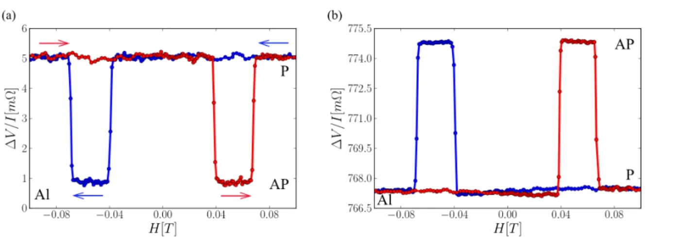
Figure 2.3(a) presents typical experimental data of V /I signal as a function of external magnetic field, recorded at T = 77 K for P y/Al based nano-device with L = 200 nm. The red curve represents a nano-structure with larger width of the non-magnetic channel (wN = 100 nm)
and the blue one stands for wN = 50 nm. The spin signal amplitude is clearly increased from 8 mΩ to 21 mΩ. One can notice a good agreement with the numerical simulations from figure
2.1, where the ratio of the spin signal amplitudes for similar nano-wires is 10/22 mΩ.
2.3
Interfaces (multi-level and multi-angle nanofabrication
meth-ods)
Apart from the geometry of the device, the second parameter, that needs to be considered for the optimization of the spin signal amplitude, is the effective spin polarization Pef f [cf. Eq. 2.1]. To optimize Pef f, the F/N interfaces have to be clean, without any contamination that could
Figure 2.2: SEM images of the Lateral Spin-Valve nano-structure made by (a) multi-angle evap-oration technique and (b) multi-level technique (cf. Section2.3). Two ferro-magnetic (F) 15 nm thick nanowires are connected by a non-magnetic (N) 60 nm thick channel. One of the magnetic stripes (F1) contains nucleation pads in order to facilitate the domain wall nucleation process leading to the lowering of its reversal field.
Figure 2.3: (a) V /I signal in the Non-Local probe configuration as a function of the external magnetic field for P y/Al nano-structures with L = 200 nm, recorded at T = 77 K. In red, data for nano-device with a 100 nm and in blue with a 50 nm wide N channel. Increase of the amplitude of the spin signal is of the order of 100%, when reducing the N channel width by a factor of 2. (b) The Non-Local and (c) GMR probe configuration schematics in LSVs.
2.3. MULTI-LEVEL AND MULTI-ANGLE METHOD ∆V /I [mΩ] T [K] L [nm] ref. Au 0.025 10 150 [45] 2 15 100(400) [75] Cu 2.5 77 250 [76] 0.7 300 200 [74] Al 1.3 4.2 250 [48]
Table 2.1: Examples of typical spin signal amplitudes ∆V /I for lateral spin-valve with Al, Cu and Au (with Py electrodes), taken from literature.
of nano-fabrication of the lateral nano-structure using lithography processes that can be used for this purpose. Both of them will be discussed in the following.
2.3.1 Multi-level method
The first, and a most used method (named the multi-level method) consists in two sets of pro-cesses: lithography, deposit and lift-off [cf. Appendix B] of the F material, followed by the same steps for the N. The first difficulty in the lithography process is that for each material the sample needs to be realigned using special realignment marks. This, eventually, brings uncontrolled shifts in the nano-device patterns, especially for the overlaps between different e-beam lithogra-phy levels. These problems are usually overcome when increasing the nano-structures size or the gap between wires (thus decreasing the spin signal amplitude). In our samples we were able to optimize the realignment conditions in order to reduce the alignment error down to 20 nm. The multi-level method brings forward another important aspect that involves the cleaning by ion milling of the ferromagnetic/non-magnetic interface before the deposition of the nonmagnetic channel. It is necessary, as the non-controlled oxidation and contamination by resist residues, leading to spin depolarization at the F/N , interface exist after the first step. This leads to the decrease of the spin signal amplitude down to its disappearance.
Several nano-structures using the same technique and similar design, with Al non-magnetic channel, were fabricated. A Scanning Electron Microscope (SEM) image of the typical nano-device is presented in Fig. 2.2(b). The widths of the ferro-electrodes and non-magnetic stripe are wF = wN = 50 nm. In this geometry, the ferro-magnetic stripes are connected by a 80 nm
thick non-magnetic Al channel.
Typical spin signal amplitudes for LSV nano-structures with transparent interfaces are pre-sented in table 2.1. The highest value reported up to now for similar type of nano-devices was achieved for Py/Cu nano-pilars type structures by Yang et al. [77] yielding 18.5 mΩ, with a shadow fabrication approach. A high spin signal amplitude was also reported for Py/Ag reach-ing up to 10 mΩ at 77 K, the reason bereach-ing high interface resistance. However, the typical values of the spin signal do not overcome 2 mΩ, according to the calculation presented in Fig. 2.1, with w = 100 nm, and in a literature overview.
Figure2.4represents the V /I signal in the Non-Local (a) and Local (b) probe configurations [cf. Fig. 2.3(b-c)] as a function of magnetic field for nano-devices made by the multi-level nanofabrication method. Before the deposition of the normal channel, connecting the two
ferro-Figure 2.4: V /I measurements in (a) Non-Local and (b) Local (GMR) probe configurations shown in Fig.2.3(b-c), recorded at T = 77 K for Py/Al nano-device made using the multi-level nano-fabrication method. The distance from center to center of the ferro-electrodes is equal to L = 200 nm. The amplitude of variation is (a) 4.16 mΩ and (b) 7.55 mΩ for Non-Local and Local configuration respectively [cf. Fig. 2.3(b-c)]. Blue and red curves correspond to positive and negative magnetic field sweep directions.
magnetic electrodes, the interface needs to be cleaned by milling. The duration of the ion-milling process has been optimized in order to obtain the highest spin signal, similarly to the work presented by Yakata et al. [78] and Jedema et al. [50]. In our approach, the optimum time was found to be 50 s using 400 V acceleration voltage. However, it can vary with the geometry of the nano-structure and with the nano-fabrication method, as the resists openings can be different for different designs. The amplitude of the spin signal yields 4.16 mΩ in NL compared to 7.55 mΩ in the GMR configuration [cf. Fig. 2.3(b-c)], at 77 K, which are the highest values reported so far using this method for Py/Al based LSV with transparent junctions [48,46,47,79,53].
In order to avoid the uncontrolled oxidation at the F/N interface, one can use the so-called shadow evaporation technique, which will be described in the following.
2.3.2 Multi-angle method
In the case of the shadow evaporation technique [36,77,80], the sample is kept in vacuum between the F and N wire depositions and hence for the F/N interface fabrication. This ensures good contacts quality, without the need of interface cleaning between the deposition of the ferromagnet and of the non-magnetic channel.
2.3.2.1 Standard shadow method
The most commonly used shadow technique is based on a bi-layer resist approach, where one uses two resists of different molecular weight [81]. The under-layer, of a lower molecular weight can be exposed and developed while the over-layer is unaffected. This results in the formation of very large undercuts due to its higher sensitivity.
2.3. MULTI-LEVEL AND MULTI-ANGLE METHOD
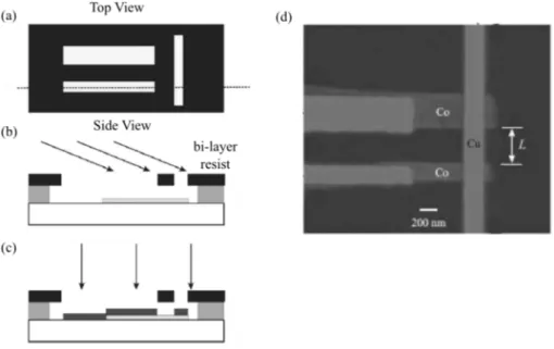
Figure 2.5: Schematic representation of the commonly used shadow evaporation technique. (a) top view of the bi-layer resist mask with patterned regions in white. (b) Deposition of one material at an angle respect to the normal direction to substrate plane. (c) Deposition of the second material using the shadowing effect of the top resist layer. (d) SEM image of typical Co/Cu nano-structure made using shadow evaporation method. Extracted from [80].
First, a bi-layer resist is deposited on a substrate [cf. Fig. 2.5(a)]. This step is followed by the e-beam insolation of the desired pattern. Then one of the two materials is evaporated at an angle with respect to the direction normal to the substrate [cf. Fig. 2.5(b)], through a bi-layer, in order to form two straight continuous nano-wires. The evaporation of the second material is done perpendicularly to the substrate plane [cf. Fig. 2.5(c)]. The top layer induces a shadowing effect which results in the gap forming two separated nano-stripes of the second material. A typical nano-structure, made by using the standard shadow evaporation technique for Co and Cu, is represented on the SEM image in Fig. 2.5(d).
The main advantage of this technique is that the active part of the structure is fabricated in the vacuum, assuring clean interfaces between the two materials. However, there are also some limitations. The nano-structure made with this method is limited in the number of terminals (3) that can connect a single junction, since otherwise the nano-device would be shortcut with the same material. Fig. 2.5(d) represents a nano-structure with three terminals connected to a single interface. Moreover, it is not possible to form small gaps between parallel wires (L in Fig.
2.5(d)). Therefore, a single resist multi-angle evaporation technique was developed for a more flexible nanofabrication approach.
2.3.2.2 Multi-angle shadow method
In this technique, one single Poly-Methyl Methacrylate (PMMA) layer is used. The central part of the device is patterned entirely in one step, using electron beam lithography without distinction between the ferromagnetic and non-magnetic wire parts. We make high aspect resist openings in
Figure 2.6: Schematic representation of the multi-angle evaporation method. High aspect ratio openings of a single resist are used for in vacuum processing of the active part of the nano-structure. (a) The central part of the device is patterned by the means of e-beam lithography, followed by (b) the evaporation of the ferromagnetic material at 30 degrees with respect to the direction normal to the substrate plane. Then (c) the sample is rotated by 90 degrees in-plane and a non-magnetic material is evaporated at 30 degrees and -30 degrees.
2.4. MATERIALS DEPENDENCE
the PMMA layer, and design the wires in a cross geometry [cf. Fig. 2.6(a)]. When depositing at a suitable angle, this allows depositing material in only one of the wire orientations, thus taking advantage of the shadowing effect in the perpendicular trenches. This approach does not need a bilayer resist, and big undercuts formation for lift-off process, as it prevents undesirable material deposition at the junction between the substrate and the resist. This allows us to build a more flexible device geometry with numerous electrodes and a much smaller gap between parallel wires (down to 50 nm in our case). Additionally, the presence of the nucleation pads on one F wire allows us to obtain a quite stable anti-parallel state, without having to increase one wire width and thus decreasing the spin signal [cf. Sec. 2.4.2].
Permalloy stripes (Py) are evaporated at an angle of 30 degrees [cf. Fig. 2.6(b)]. Since trenches in the PMMA are 300 nm deep and their maximum width is 140 nm (the reservoir), all trenches perpendicular to the deposition axis are protected against deposition by a shadow effect. Then the sample is rotated in its plane by an angle of 90 degrees, and the non-magnetic material (Al, Cu or Au) is deposited with the same 30 degree angle [cf. Fig. 2.6(c)]. This time, however, one needs to evaporate from both directions in order to avoid the formation of a gap due to the shadowing effect by the first deposit. This can be done using sequences of evaporations at +/-30 degrees. All wires have a sharp apex to limit the deposition of the material on the side of the resist, thus facilitating the lift-off process.
This technique allows for the formation of ultra-clean interfaces. The microscopic Ti(5 nm)/Au(100 nm) contact electrodes are either deposited before or after the fabrication of the active part of the device.
2.4
Materials dependence
Beyond the reduction of the wire width to increase the spin resistances, and the development of techniques for in-vacuum interface fabrication, the third parameter that can be changed to maximize the spin signal amplitude is the choice of materials. This parameter turns out to manifest itself through the terms Pef f, ρN (F ) and lsfN, which are present in the resistance ratio and in the hyperbolic sinus part of Eq. 2.1. By using a non-magnetic material with short lNsf and thus low spin resistance, as in Au [37], the spin resistance ratio and thus the spin signal could be increased as it will be easier to inject spins into N. However, there is an opposite effect of lNsf on the spin signal, which comes from the [sinh( L
lN sf
)]−1 factor. We thus choose to study Al and Cu, which possess long lsfN, and compare these materials to Au.
2.4.1 Spin signal for different materials
Measurements were performed at room temperature and at 77 K with the magnetic field oriented along the ferromagnetic wires. Three types of nano-structures were studied, based on Al, Cu and Au non-magnetic channel, fabricated by the multi-angle evaporation method.
The V /I non-local signal as a function of magnetic field is shown in Fig. 2.7(a), for an Al-based LSV at 77 K. For this LSV, the center to center distance L between the injector and
Figure 2.7: Non-local magneto-transport measurements for three types of Lateral Spin-Valves with (a) Al, (b) Cu, (c) Au non-magnetic channel. Data-points were recorded at T = 77 K for the same nano-devices geometry: L = 150 nm (distance from center to center of the ferromagnetic electrodes), with nano-wires of 50 nm width. (d) Comparison of the spin signal amplitudes from three N materials. The red line representing the highest value reported in the literature [77].
2.4. MATERIALS DEPENDENCE
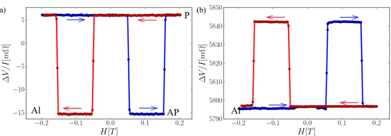
Figure 2.8: V /I measurements in (a) the Non-Local and (b) Local (GMR) probe configurations (shown in Fig.2.3(b-c)) recorded at T = 77 K, for Py/Al nano-device made using the multi-angle evaporation method. The distance from center to center of the ferro-magnetic electrodes is equal to L = 200 nm.
the detector is equal to 150 nm. A clear spin signal can be seen, with a well-defined plateau in the anti-parallel magnetization state of the ferromagnetic electrodes. The spin signal is equal to ∆V /IAl = 24 mΩ, which is the highest value reported up to now for ohmic interfaces by Yang et
al. [77], yielding 18 mΩ, by mixing pillar nanofabrication and lateral connection in vacuum. Moreover, this result is in agreement with the GMR measurements (local detection) presented in Fig. 2.8(b) for L = 200 nm, where the resistance change for GMR is of 48 mΩ instead of 21 mΩ for the spin signal of Fig. 2.8(a). Note that the GMR/spin signal ratio is close to the expected value of 2, which corresponds to the sum of the spin signals at the two identical interfaces [82]. Note that in the Non-Local configuration the current path and the voltage lines are a little bit more separated than in the local GMR measurement, which may explain why the ratio is a little bit smaller than 2.
Spin signal measurements were also performed for Cu-based devices, with L = 150 nm. Clear spin signals were observed, up to 9 mΩ at room temperature [cf. Fig. 2.9(b)] and 21 mΩ at 77 K [cf. Fig. 2.7(b)]. Interestingly, for Py/Cu, made by the multi-level method, we obtained very recently signals up to 18 mΩ, demonstrating a very good cleaning of the F surface.
For Au-based devices, and still with a width L of 150 nm, a much smaller spin signal amplitude was observed, the magnitude being of the order of 1.5 mΩ [cf. Fig. 2.9(a)] and 5.5 mΩ [cf. Fig.
2.7(c)] at 300 K and 77 K respectively. Also, the small spin signals obtained using Au can be accounted by the equations of 1D models for the case of Ohmic contacts: the amplitude of spin signals is mostly governed by the sinh part of the equation, even for as small as possible L/lsf ratio. Note that in the case of Au L > lAusf .
The ratios in amplitudes of the spin signals between the liquid nitrogen and room tempera-tures of almost 3.5 times for Au and 2.3 times for Cu come from the decrease of lNsf and Pef f., when going from 77 K to 300 K. In this case, the scattering mechanism [cf. Chapter 1] of the spins on phonons becomes dominant, resulting in shorter spin diffusion lengths, smaller effective


![Figure 2.10: Numerical simulations using simple 1D spin diffusion model [14] of (a) the spin signal amplitude as a function of R N and l sfN](https://thumb-eu.123doks.com/thumbv2/123doknet/12871868.369343/44.892.131.804.134.420/figure-numerical-simulations-simple-diffusion-signal-amplitude-function.webp)