HAL Id: cea-02432952
https://hal-cea.archives-ouvertes.fr/cea-02432952
Submitted on 8 Jan 2020
HAL is a multi-disciplinary open access
archive for the deposit and dissemination of
sci-entific research documents, whether they are
pub-lished or not. The documents may come from
teaching and research institutions in France or
abroad, or from public or private research centers.
L’archive ouverte pluridisciplinaire HAL, est
destinée au dépôt et à la diffusion de documents
scientifiques de niveau recherche, publiés ou non,
émanant des établissements d’enseignement et de
recherche français ou étrangers, des laboratoires
publics ou privés.
A miniaturized optical sensor for particulate matter
detection
Maryse Fournier, Pierre Barritault, Gabriel Jobert, Adrien Marchant, Salim
Boutami, Julien Michelot, Pierre Lienhard, Sergio Nicoletti, Laurent
Duraffourg
To cite this version:
Maryse Fournier, Pierre Barritault, Gabriel Jobert, Adrien Marchant, Salim Boutami, et al.. A
miniaturized optical sensor for particulate matter detection. Photonics West 2020, SPIE, Feb 2020,
San Francisco, United States. �10.1117/12.2546128�. �cea-02432952�
A miniaturized optical sensor for particulate matter detection
Maryse Fournier
a, Pierre Barritault
a, Gabriel Jobert
a, Adrien Marchant
a, Salim Boutami
a, Julien
Michelot
b, Pierre Lienhard
b, Sergio Nicoletti
a, Laurent Duraffourg
aa
Université Grenoble-Alpes, CEA-LETI Minatec, F38000 Grenoble, France;
b
Pyxalis, Moirans, France
ABSTRACT
We present an innovative optical particulate matter sensor. This optical sensor ‘on-a-chip’ combines a visible fibered light source and a custom-made CMOS image sensor chip. By illuminating a single particle in an air channel, we can record the light scattering signature on the photodiode matrix. A piece realized in 3D printing achieves fiber alignment and an efficient stray light protection.
A specific scattering pattern occurs from the interaction of light with a single particle. Unlike traditional optical PM sensors based on a single photodiode detection, we measure a lens-free projection of the scattering signature on the nearby image sensor (1.5mm projection distance). This allows us to count particles and determine their size and refractive index. These parameters are retrieved through image processing and by comparison with a radiometric model that calculates the projection of a Lorenz-Mie’s scattering pattern.
We describe the sensing technique, the architecture and fabrication of this sensor as well as the characterization results, which are in good agreement with our theory-based predictions. In particular, we show that it is possible to differentiate calibrated particulates of different sizes (monodisperse polystyrene-latex spheres). The sensor is sensitive enough to detect single particle and smallest than 1µm.
Keywords: Particulate matter, optical sensor, PM1, light scattering, Lorenz-Mie theory, CMOS image sensor, detector, PM2.5, air quality sensor, PM 0.2
1.
INTRODUCTION
Air pollution has significant effects on health and the environment. Despite a trend towards improved air quality over the past twenty years, limit values are still not respected in several areas and countries. Particulate Matter (PM) is a class of pollutant known to have serious medical impacts [1]. It is composed of suspended particles or liquid droplets, from natural (volcano dust, bacterium, pollens etc.) or anthropic origin (industrial combustion, cigarette smoke) and of size ranging from a few nanometers to a few micrometers. The size of particle is related to how deep it penetrates the human body and thus linked to their potential for causing health problems. They are categorized into different classes along their sizes [2]. In particular, class PM2.5 (particles smaller than 2.5µm) have been classified as a known carcinogenic agent (group 1) by the IARC (International Agency for Research on Cancer) [3]. PM1 (submicronic particle inferior to 1µm) is expected to be more dangerous than PM2.5 [3] [4] . PM with diameter inferior to 200nm have also been observed in the brain, and it could be linked to neurodegenerative diseases, as Alzheimer’s disease [5].
So there is an important need for being able to monitor air quality, with obviously the final intention of regulating it [6]. It exists a lot of different principles of measurement techniques and associated sensors [7] . Classical light scattering in the visible range does measuring PM concentration. Indeed, the scattering process is increasing when light wavelength is decreasing. Recent works show miniaturization of such sensors using microfabrication techniques and co-integration of light sources, photodetectors and fluidics [8] [9].
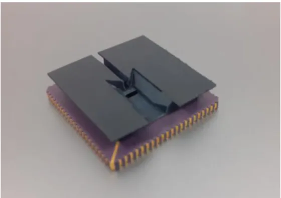
The purpose of this work relies on a new sensor, portable, low cost and measuring PM in real time. It is micro fabricated from a CMOS wafer. Hereinafter in Figure 1, we present the photography of the miniaturized final device that allow a complete signature of both forward and backward scattered diagrams of PM.
Figure 1: Photography of a miniaturized optical particulate sensor
2.
THEORY AND SENSING TECHNIQUE
The phenomenon of light scattering is commonly described by the theory of Lorenz-Mie [10]. This is a specific solution of Maxwell’s electromagnetic equations for a spherical particulate (no matter the diameter range), with a complex refractive index and illuminated by a monochromatic plane wave as represented in Figure 2
Figure 2: Mie scattering of a small particle
One can detect the scattered light of particle with a diameter smaller than a few microns, can analyze the scattered light and then classify the particle [11]. Each particle be defined by its shape, its size and has a refractive index depending on the material of which it is made up. From the illumination conditions, one can predict the absorbed optical power and the scattered signature of the particle, the latter being the scattering intensity as a function of the scattering angle (angle between the incident light and the scattered ray).
It is important to measure this angular dependent scattering track to try to determinate precisely the optical and geometrical properties of the unknown particles.
The Lorenz-Mie theory shows that larger particles presents several scattering angular lobes of higher intensity and their number is strongly dependent of the refractive index of the particulate matter. For a same kind of particle, we can go back to the size of the particles diameter as it increased with the number of lobes.
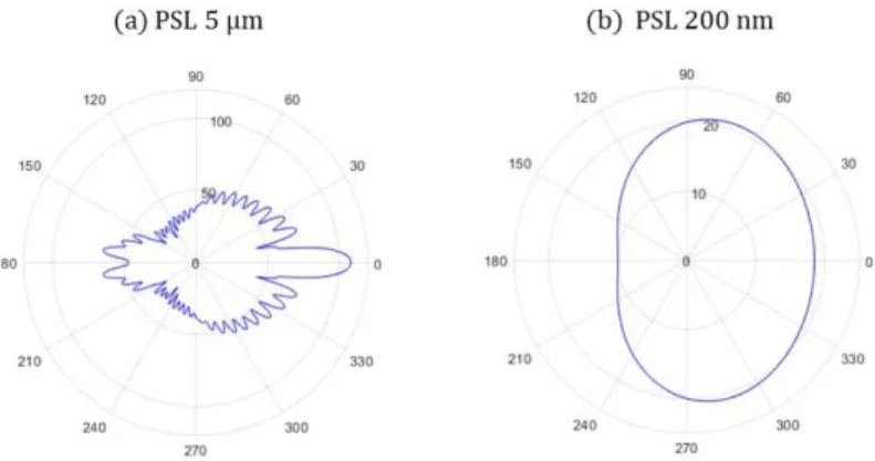
Figure 3 shows an example of polar plot with our house Lorenz-Mie Model calculating the interaction between an incident beam constituted by a plane wave of wavelength of 635nm and a single spherical particle PSL (PolyStyrene Latex) with a refractive index of 1.59 at this wavelength.
Figure 3: Example of polar plot (log scale) showing the use of the Lorenz-Mie theory for scattering light (λ=635nm) with particle PSL at two different diameters
With our novel imager sensor, we capture a angular scattering signature by a direct projection of the scattered light on the imager detection matrix.The particle interact with the illumination beam in a fluidic channel situated at the center of the detection matrix and at a near distance of the photodiodes. This proximity ensures a high field of view of all scattering angles and a good sensitivity without using any additional optical element (e.g. mirrors or lenses).
Thus, this method allows differentiating types of particle cloud by estimating size and refractive index at very low concentration. For this purpose, we have developed an analytical model, which predict the signature projected on the focal plane of the detector in function of the nature of particle and its size. In this model, we consider the particle spherical and illuminated by a non-polarized monochromatic planar wave. The projection of scattered rays is calculated by classic radiometric optic for each pixel of the detection matrix.
We show in the characterization chapter, examples of images from the model compared to experimental data.
3.
DEVICE ARCHITECTURE
A first developed version gave only a partial signature of the polar scattering diagram [12] [13]. Figure 4 shows a schematic view of the new architecture of optical PM sensor who gives the scattering signature with wider field of view. Two parts compose the device. The upper grey part (a) is a light chamber that we call a cloaker made in black resist with a high-resolution 3D printing equipment by Formabs (Form 2). We designed the cloaker in order to allow the light beam closest to the fluidic channel. In this way, we have as little stray light as possible to avoid the glare of the detection pixels on the focal plane. Due to the experimental configuration, we had to bring the light from a SLED with its driving electronics towards the motherboard, through an optical fiber. The carrier of the experimental sensor is clipped on to the prototype motherboard that drives the CMOS imager. The optical fiber is held in a groove for a perfect fixation. A large funnel serves as a channel to guide the particles towards the detection volume.
The black lower part (b) is an imager from a standard platform proposed by Pyxalis, an ultra-fast pixel, from a prototyping test vehicle. This platform is designed to be extreme flexible and quickly modified with limited effort and at lower cost. This test vehicle is delivered with driving software, an USB connection to a standard PC and DLLs to interface with Matlab software and allow us to control our imager with great flexibility.
The layout of the chip has been modified to our custom need to create a blind area, which allows drilling the fluidic channel at the center of the detection matrix. The imager chip layout is presented in Figure 5. It size is 6 mm x 5.9 mm, is composed of a core part and a frame part. The core part is divided in two detections areas of 75x280 pixels: the ‘forward matrix’, which detects the scattered light in the forward direction whereas the ‘backward matrix’ detects the backscattered light. The designed blind area has a size of 2 mm x 0.5 mm, with a rectangular profile. This area free of pixels or routing lines is surrounded by a seal ring to allow the creation of the fluidic channel with less degradation as possible of the photodiodes situated near the drilling area.
Figure 5: Imager chip layout
The 10 microns pixel is designed with a typical 2 gains high dynamic range, 5T architecture allowing a low noise Global-Shutter (GS) or Rolling-Shutter readout procedure [14]. They ensure good sensitivity at low intensity scattered light. This drilled CMOS imager is packaged on a drilled standard LCC84 ceramic chip carriers whose size is less than 3 cm x 3cm. The carrier is plugged, with full contact on the electronic motherboard socket called CreaPYX test platform as represented in Figure 6, below.So the channel allows the circulation of particulate matters that are set in motion by forced convection. Particles are illuminated by the light beam coming out from the fiber, placed nearby the outlet of the channel. Thus, the CMOS imager driven by the software captures the complete images of the scattered diagram of the particles that pass through the channel.The post-processing of the images will then allow us to determine the size, number and type of particles. This will not be discussed in this article.
4.
FABRICATION
4.1. Imager chip
We supplied the 8 inch Imager CMOS wafers from a shuttle run of a specialized advanced manufacturing fab.
4.2. Drilled Imager chip
To drill the wafers we need to use microfabrication technologies that are widely used today in manufacturing and laboratory research. Most of microelectronics and micro technology predominantly use silicon as a substrate material; it can be etched quickly and manufactured at a low cost for mass production.
We have developed a post-process in our 200 mm MEMS foundry to drill the components at wafer scale and fully compatible with standard microelectronics processes. An external seal ring is commonly implemented outside the chip. Here, we also added an internal seal ring designed to protect the matrix of photodetectors during the drilling process. At first, we use a front side process to etch the multilayer passivation on top of the wafer. We use a 365nm-stepper for the lithography to align the oblong holes mask on the alignment mark included on the wafer and we etch the passivation with a C4F8/CO plasma process in a reactor of a Reactive Ion Etching (RIE) equipment. After protecting the front side by a film, we finalize by a backside process to etch the total thickness of the bulk silicon. We deposit a few microns of oxide hard mask by PECVD equipment and use a contact photolithography on a positive resin, the oblong hole pattern has a dimension of 2000 µm x 500 µm. Usually the deep anisotropic etching is limited above 500 μm in our case the bulk silicon thickness to etch is 725µm, for this point, we use a well-known equipment: an inductively coupled plasma-deep reactive ion etching (ICP-DRIE). The inductively coupled plasma (ICP) reactor has been thus widely used for anisotropic silicon etching because it is able to obtain a high aspect ratio while maintaining a vertical sidewall and by deep reactive ion etching (DRIE) technology, the silicon substrate can be etched faster. Recent works show the interest of using this microfabrication technique[15]. In our case, there is not a difficult Aspect Ratio AR=1.45, we use a standard Bosh process to obtain a straight profile. This process consist of the alternative and cyclic isotropic etching with SF6 gaz followed by C4F8 plasma to create a protection layer on the sidewalls. We obtained fluidic channel with straight profile and with small scalloping on the sidewall.
Figure 7: Fabricated holed imager chip at wafer scale
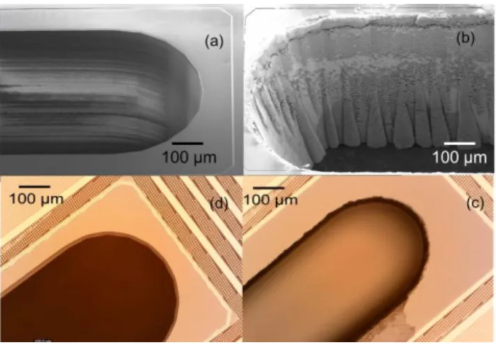
Alternatively, we demonstrated that it is also possible to create the fluidic channel at wafer level by high power ultrafast fiber laser. The results were obtained only on a first trial and on a few samples in this work and the process could be significantly improved if necessary. We observed on the photography in Figure 8(c) that some burned residues of the protective resin could not be removed by standard acetone solvent spraying. Even if we observe sidewalls roughness much more important in the part of bulk silicon Figure 8(b), the CMOS chips functioned and we could test them.
Figure 8: comparison of drilled hole obtained by DRIE or laser technology ;(a) (d) SEM and microscopy view of DRIE process; (b) (c) SEM and microscopy view of Laser process
4.3. Impact estimation of the drilling process
We have designed the pixels in order to have good sensitivity at low intensity scattered light with low noise.
We observe saturated hot pixels at the internal edges (central white lines), caused by a higher photodiodes dark current on a few lines near the seal ring. These defective lines will not be taken into account in our image acquisitions. In order to estimate the impact of the drilling process on the dark current of the image sensor, we made cartographies of the dark current before and after the both drilling steps. We obtained a dark current map by recording and average images for different integration times and following the intensity of one pixel, we were able to deduce its dark current. At the end, we conclude that the drilling post process had an effect on dark current (DC). The DC level was increased of about 30%. We also notice no evidence of gradient in noise distribution, which might have been expected as a drawback of the drilling process. We conclude that we obtained very similar results for both drilling technics (DRIE and laser drilling). As the dark current increase is not a critical parameter for our need because we use short integration time. The most important parameters for our application is the readout noise which is quite low σR = 3.4 e- rms for our sensor.
5.
CARACTERIZATION RESULTS
5.1. Sensor setup
The chip was wire-bonded to the drilled ceramic carrier and plugged into the test CreaPIX platform, we install the 3D printed cloaker on top of the carrier. Beforehand we have inserted in the groove, the single mode lensed optical fiber. We connect the pigtail to a SLED, delivering an optical Power of 1mW, at visible wavelength of 635nm.
Thus, we illuminate a detection volume really close to the output fluidic channel at a distance of 1.5mm between the optical axis and the focal plane of the photodiodes. This proximity allows for a good sensitivity to scattered light and a quite wide field of view of scattering angles.
5.2. Experimental setup
We generate in a confined area, a controlled flow of particles by an aerosol dispenser (Constant Output Atomizer Model 3076 by TSI). We use commercial solutions of calibrated particles with different diameters: Polystyrene Latex Spheres (PSL) with monodisperse distribution of their diameter. We use a bypass tube to send particles to a reference equipment (APS Spectrometer 3321 by TSI). The flow directed toward our sensor has a flow rate of 0.8 L/min. The particulate matter flow through the entire holed sensor and the illumination beam. Each particle that interact with the light beam print his own track on the recorded images driving by the software. We capture 32 images in burst mode with an integration time of 5ms. The imager functions in global shutter low noise mode; this mode is important to capture a complete scattered signature from a moving particle. We have developed our in-house program to keep only images where a signal is detected from a threshold value based on standard deviation on the forward image. Of course, a
background image subtraction (with an image recorded with no particle in the illumination beam) is automatically performed in the routine.
5.3. Experimental Result
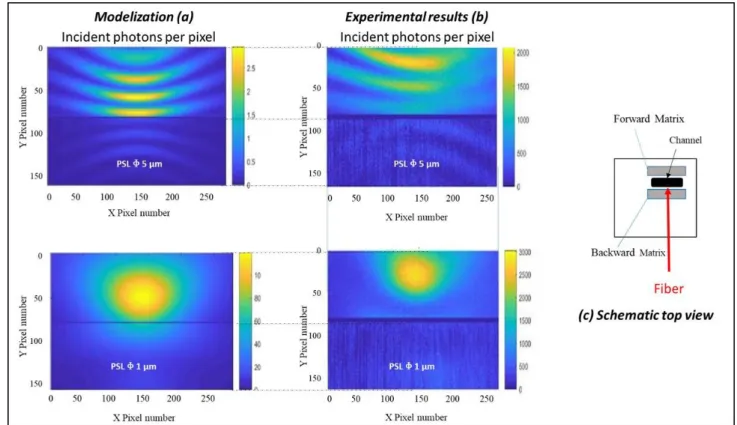
We succeed to measure with our novel sensor complete angular scattering signatures for different diameter sizes of PSL from 200nm to a few microns that will be present in a future work. We present here in Figure 9 below, complete scattering diagrams of particles obtained with our new miniaturized sensor compared to modelization. That shows a clear dependence with the size of particles, in good agreement with analytic modeling. We observe in experimental measurements (b) of Figure 9, two luminous lobes structured with fringes in forward matrix area and two less luminous in the backward area. For PSL with diameter 1 microns, we see that the signature has not a few fringes but only one spherical lobe and more intense. The intensity and number of fringes (side scattering lobes) increases with particle diameter.
Figure 9: comparison modelization (a) Versus experimental results; (b) for two different diameters of PSL particles; (c) schematic top view of the detection system
It is quite similar but not exactly identical to modeling. It may be due to a dispersion in PSL diameter typically 10% (intrinsic to the available samples), and that we estimate the refractive index at our wavelength λ = 635 nm as nPSL = 1.59. We also do not know the velocity and the position of the particles when their signature are captured.
We start to develop an in-house program to retrieve the parameters through image processing and then could identified, size, concentration and type of particulate matter by comparison with a radiometric model calculating the projection of a Lorenz-Mie’s scattering pattern.
6.
CONCLUSION & PERSPECTIVES
In conclusion, we have demonstrated the interest to create a fluidic channel situated at the center of a matrix of photodiodes of a CMOS imager covered by a cloaker that bring the light beam. This miniaturized and very sensitive sensor is capable to capture one scattered image of a particulate matter of very small size, less than 1µm, who flow through its fluidic channel.
In future developments, we hope to respond to the various improvements identified such as new fluidic set up to define particle’s position and its velocity, reduce stray light in the cover, development of image processing that implement the simultaneous analysis of both forward and backward matrixes. We could imagine a near future with this new low-cost sensor that looks promising as a cheap solution to measuring PM in the home, workplace or outdoor pollution.
ACKNOWLEDGEMENTS
The authors are thankful to the fabrication and packaging teams from CEA-LETI who help us to develop recipe process to drill the chip and for bonding the CMOS imager on top of the holed ceramic.
REFERENCES
[1] G. B. Hamra et al., “Outdoor Particulate Matter Exposure and Lung Cancer: A Systematic Review and Meta-Analysis,” Environ. Health Perspect., vol. 122, no. 9, pp. 906–911, Sep. 2014, doi: 10.1289/ehp/1408092.
[2] J. O. Anderson, J. G. Thundiyil, and A. Stolbach, “Clearing the Air: A Review of the Effects of Particulate Matter Air Pollution on Human Health,” J. Med. Toxicol., vol. 8, no. 2, pp. 166–175, Jun. 2012, doi: 10.1007/s13181-011-0203-1.
[3] A. J. Cohen, “Air pollution and cancer.” 2017.
[4] P. Vineis and K. Husgafvel-Pursiainen, “Air pollution and cancer: biomarker studies in human populations †,”
Carcinogenesis, vol. 26, no. 11, pp. 1846–1855, Nov. 2005, doi: 10.1093/carcin/bgi216.
[5] B. A. Maher et al., “Magnetite pollution nanoparticles in the human brain,” Proc. Natl. Acad. Sci., vol. 113, no. 39, pp. 10797–10801, Sep. 2016, doi: 10.1073/pnas.1605941113.
[6] E. G. Snyder et al., “The Changing Paradigm of Air Pollution Monitoring,” Environ. Sci. Technol., vol. 47, no. 20, pp. 11369–11377, Oct. 2013, doi: 10.1021/es4022602.
[7] S. Amaral, J. de Carvalho, M. Costa, and C. Pinheiro, “An Overview of Particulate Matter Measurement Instruments,” Atmosphere, vol. 6, no. 9, pp. 1327–1345, Sep. 2015, doi: 10.3390/atmos6091327.
[8] S. D. Lowther, K. C. Jones, X. Wang, J. D. Whyatt, O. Wild, and D. Booker, “Particulate Matter Measurement Indoors: A Review of Metrics, Sensors, Needs, and Applications,” Environ. Sci. Technol., vol. 53, no. 20, pp. 11644–11656, Oct. 2019, doi: 10.1021/acs.est.9b03425.
[9] M. Dong, E. Iervolino, F. Santagata, G. Zhang, and G. Zhang, “Silicon microfabrication based particulate matter sensor,” Sens. Actuators Phys., vol. 247, pp. 115–124, Aug. 2016, doi: 10.1016/j.sna.2016.05.036.
[10] T. Wriedt, “Mie Theory: A Review,” in The Mie Theory, vol. 169, W. Hergert and T. Wriedt, Eds. Berlin, Heidelberg: Springer Berlin Heidelberg, 2012, pp. 53–71.
[11] C. F. Bohren and D. R. Huffman, Absorption and scattering of light by small particles. Weinheim: Wiley-VCH, 2009.
[12] NICOLETTI SERGIO, “Particle detector and method for producing such a detector,” US8867035 B2 2014-10-21 [US8867035]-US20130120749 A1 2013-05-16 [US20130120749]-EP2596329 B1 2013-02-15 [FR2963101]-FR2963101 A1 2012-01-27 [FR2963101].
[13] S. Boutami et al., “Visible to mid-infrared integrated sensors for air quality measurement,” 2019, p. 25, doi: 10.1117/12.2529262.
[14] B. Dupont et al., “A dual-core highly programmable 120dB image sensor,” Electron. Imaging, vol. 2016, no. 12, pp. 1–3, Feb. 2016, doi: 10.2352/ISSN.2470-1173.2016.12.IMSE-261.
[15] E. Herth et al., “Fast ultra-deep silicon cavities: Toward isotropically etched spherical silicon molds using an ICP-DRIE,” J. Vac. Sci. Technol. B, vol. 37, no. 2, p. 021206, Mar. 2019, doi: 10.1116/1.5081503.