HAL Id: hal-01507361
https://hal.archives-ouvertes.fr/hal-01507361
Submitted on 28 Apr 2017
HAL is a multi-disciplinary open access
archive for the deposit and dissemination of
sci-entific research documents, whether they are
pub-lished or not. The documents may come from
teaching and research institutions in France or
abroad, or from public or private research centers.
L’archive ouverte pluridisciplinaire HAL, est
destinée au dépôt et à la diffusion de documents
scientifiques de niveau recherche, publiés ou non,
émanant des établissements d’enseignement et de
recherche français ou étrangers, des laboratoires
publics ou privés.
Alignment control and atomically-scaled heteroepitaxial
interface study of GaN nanowires
Qingyun Liu, Baodan Liu, Wenjing Yang, Bing Yang, Xinglai Zhang,
Christophe Labbe, Xavier Portier, Vladimir An, Xin Jiang
To cite this version:
Qingyun Liu, Baodan Liu, Wenjing Yang, Bing Yang, Xinglai Zhang, et al.. Alignment control and
atomically-scaled heteroepitaxial interface study of GaN nanowires . Nanoscale, Royal Society of
Chemistry, 2017, pp.5212-5221. �10.1039/C7NR00032D�. �hal-01507361�
PAPER
Cite this:Nanoscale, 2017, 9, 5212
Received 3rd January 2017, Accepted 17th March 2017 DOI: 10.1039/c7nr00032d rsc.li/nanoscale
Alignment control and atomically-scaled
heteroepitaxial interface study of GaN nanowires
†
Qingyun Liu,
a,bBaodan Liu,
*
aWenjin Yang,
aBing Yang,
aXinglai Zhang,
aChristophe Labbé,
cXavier Portier,
cVladimir An
dand Xin Jiang*
aWell-aligned GaN nanowires are promising candidates for building high-performance optoelectronic nanodevices. In this work, we demonstrate the epitaxial growth of well-aligned GaN nanowires on a [0001]-oriented sapphire substrate in a simple catalyst-assisted chemical vapor deposition process and their alignment control. It is found that the ammoniaflux plays a key role in dominating the initial nuclea-tion of GaN nanocrystals and their orientanuclea-tion. Typically, significant improvement of the GaN nanowire alignment can be realized at a low NH3flow rate. X-ray diffraction and cross-sectional scanning electron
microscopy studies further verified the preferential orientation of GaN nanowires along the [0001] direc-tion. The growth mechanism of GaN nanowire arrays is also well studied based on cross-sectional high-resolution transmission electron microscopy (HRTEM) characterization and it is observed that GaN nano-wires have good epitaxial growth on the sapphire substrate following the crystallographic relationship between (0001)GaN∥(0001)sapphire and (101¯0)GaN∥(112¯0)sapphire. Most importantly, periodic misfit
dis-locations are also experimentally observed in the interface region due to the large lattice mismatch between the GaN nanowire and the sapphire substrate, and the formation of such dislocations will favor the release of structural strain in GaN nanowires. HRTEM analysis alsofinds the existence of “type I” stack-ing faults and voids inside the GaN nanowires. Optical investigation suggests that the GaN nanowire arrays have strong emission in the UV range, suggesting their crystalline nature and chemical purity. The achievement of aligned GaN nanowires will further promote the wide applications of GaN nanostructures toward diverse high-performance optoelectronic nanodevices including nano-LEDs, photovoltaic cells, photodetectorsetc.
Introduction
Semiconductor nanostructures with crystalline quality and good alignment have been extensively explored as ideal building blocks for various nanoscale electronic and photo-nic applications.1–3The nanostructure geometry with advan-tages of a large surface-to-volume ratio and low dimensions shows intriguing optoelectronic properties superior to their
thin-film and bulk counterparts. The representative examples of nanostructure applications, such as high efficiency solar cells made from ordered arrays of silicon nanowires,4 high performance photoelectrodes constructed from p-type silicon wire-arrays5 or 3D ordered Au/B–ZnO nanowires6for solar energy conversion and the hierarchical assembly of one-dimensional nanostructures into well-defined functional networks,7 are often reported in the literatures. Particularly, crystalline GaN nanostructures in the forms of nanowires, nanotubes and nanorods are employed in the context of specific applications such as field-emission transistors (FETs), nano-lasers, light-emitting diodes (LEDs) and overall water splitting photocatalysts due to their high electron mobility, tunable direct band-gap and excellent photoelectric sensitivity.8–15 For GaN crystals, two polymorphs like thermodynamically favorable wurtzite and metastable zinc-blende type structures are generally observed. The wurtzite GaN has an anisotropic crystal struc-ture, and many of its properties are closely dependent upon the crystal orientation.16,17 In particular, crystalline GaN nanowire arrays with good alignment have attracted extensive
†Electronic supplementary information (ESI) available: Experimental set-up, photograph and SEM images, VLS growth model, atomic structure and line-scan elemental profiles of GaN nanowires. See DOI: 10.1039/c7nr00032d
aShenyang National Laboratory for Materials Science (SYNL), Institute of Metal Research (IMR), Chinese Academy of Sciences (CAS), No. 72, Wenhua Road, Shenhe District, Shenyang 110016, China. E-mail: [email protected], [email protected]
bUniversity of Chinese Academy of Sciences, 19 A Yuquan Road, Shijingshan District, Beijing, 100049, China
cCIMAP CNRS/CEA/ENSICAEN/Normandie University, 6 Bd Maréchal Juin, 14050 Caen Cedex 4, France
dInstitute of High Technology Physics, National Research Tomsk Polytechnic University, 30 Lenin Ave., 634050 Tomsk, Russia
research interest due to their strain relieving properties, enhanced sidewall emission by exposure of different facets, and increased light output and extraction efficiency. Typically, by virtue of their nanometer scale size and distinct growth mechanism,18 vertically-oriented GaN nanowires accommodate strain at the growth heterointerfaces, reducing the density of threading dislocations which otherwise act as non-radiative recombination centers leading to an internal quantum efficiency decrease.19
To obtain vertically aligned GaN nanowire arrays, several synthetic strategies have been developed in the past few years. For instance, earlier studies demonstrated that vertical GaN nanowires with a confined nucleation location, diameter and orientation can be obtained using a patterned SiO2mask fabricated by interferometric lithography or with an anodic aluminum oxide (AAO) mask.20,21In this way, the GaN nano-wires show uniform dimensional sizes and excellent align-ment, which are accurately defined by the mask pore size and depth. However, the removal of SiO2or AAO masks is strenu-ous and occasionally destroys the GaN nanostructures. The molecular beam epitaxy (MBE) technology can also produce well-aligned GaN nanowires or nanorods with decent crystal quality and chemical purity on a variety of substrates through slow and precise Ga and N precursor control.22,23 The GaN nucleation sites can also be well defined when a thin mask is used. For example, position-controlled growth of GaN nano-wires and nanotubes can be prepared by means of MBE on a thin titanium mask structured diamond.24The Ti masks with periodic holes allow for the tuning of the diameter and inter-val distances of the nanowire arrays. Similar GaN nanowire array synthesis can also be achieved by metal organic chemi-cal vapor deposition (MOCVD) and the alignment control of GaN nanowires can be easily realized on the basis of complex optimization of precursor pressure and distribution manipu-lations.25,26 The key problem of the above-mentioned MBE and MOCVD growth of GaN nanowire arrays comes from the ultra-high vacuum and the complicated control process, which makes the aligned GaN growth more challenging. As an alternative strategy, the catalytic epitaxy of GaN nanowires on a suitable crystalline substrate has been demonstrated as feasible from the viewpoint of either theoretical or experi-mental studies. The close lattice constants of GaN and sub-strates (sapphire, SiC, ZnO, etc.) enable a direct epitaxy nucleation of GaN nanocrystals and their orientation can be directly governed by the initial substrate orientation. Typical examples of epitaxial GaN nanowire arrays can be found in wurtzite GaN nanowires in the orthogonal [11ˉ0] and [001] directions epitaxially grown on (100)γ-LiAlO2and (111) MgO single-crystal substrates.18 Among them, the sapphire sub-strate is most widely adopted in GaN epitaxial growth due to its close crystal structure symmetry and low production cost. Many advantageous applications can be expected from the scalable production of GaN nanowires with good alignment. For instance, the Wang group27proposed that GaN nanowire arrays are the ideal candidates for the homoepitaxial growth of high-quality GaN crystals with reduced threading
dis-location density. In addition, GaN nanowire arrays on a c-plane sapphire substrate also demonstrate great potential in optoelectronic applications.28,29However, the alignment uni-formity of GaN nanowires on the sapphire substrate syn-thesized from catalytic and epitaxial routines becomes more challenging with the enlargement of substrate size, which requires urgent improvement for the building of scalable optoelectronic nanodevices.
Over the past few years, our group has made considerable efforts toward the nucleation design, crystallographic align-ment control, structural defect depression and cathodolumi-nescence study of GaN nanowires processed by CVD methods.30–33Though single-crystalline GaN nanowire arrays grown along specific crystallographic directions have been successfully obtained with or without the assistance of metal catalysts, the realization of homogeneous GaN nanowires with superior alignment on an industrially scalable substrate still remains a challenge. Particularly, with the enlargement of the substrate size, GaN nanowires with different orien-tations will appear and the alignment uniformity of GaN nanowires becomes poor, which will affect the integration of GaN-based nanodevices and performance stability. As a result, it is essential and technologically important to further improve the alignment homogeneity of GaN nanowires. In this work, we demonstrate a tremendous step toward the synthesis of highly-ordered GaN nanowire arrays on a 20 × 20 mm scalable sapphire substrate. Most importantly, it was found that the crystallographic growth direction of GaN nano-wire arrays is closely related to the NH3flowing rate and a low NH3 flowing rate can lead to a significant improvement of GaN nanowire alignment. X-ray diffraction measurement con-firms the preferential orientation of GaN nanowires along the [0001] direction and a high-resolution transmission electron microscopy (HRTEM) study on the GaN/sapphire interface suggests that the GaN crystal is directly nucleated on the sap-phire surface to generate epitaxial growth. However, periodic dislocation is also observed in the GaN/sapphire interface to release the structural strain due to the lattice mismatching. A photoluminescence study on the well-aligned GaN nano-wires found a sharp emission band with a maximum peak centered at 385 nm and a weak dome in the visible range. The realization of scalable GaN nanowires with good align-ment paves a solid way toward the integration of GaN-based optoelectronic nanodevices such as nano-LEDs, UV-photo-detectors and self-powered nano-generators.
Experimental section
The highly-ordered GaN nanowire arrays were fabricated via a simple chemical vapor deposition process, as described in our previous work.33The [0001]-orientated sapphire substrate pre-viously coated with a 5 nm Au layer by an electron beam depo-sition method was used as the nucleation site of GaN nano-wires.31 High purity gallium oxide (Ga2O3) powders and ammonia gas were employed as the precursors for the
for-mation of GaN crystals. An alumina boat with Ga2O3powder was placed in the center of a quartz tube heated in a horizontal tube furnace (Fig. S1†). The temperature was increased to 1100 °C from room temperature to promote the decomposition of the Ga2O3powder and NH3 gas at a flowing rate of 10–50 standard-state cubic centimeter per minute (sccm) was intro-duced into the growth chamber from the beginning of the temperature increase. The growth of GaN nanowires was main-tained at 1100 °C for a certain period of time and then cooled down to room temperature under the protection of flowing Ar gas (100 sccm). The morphologies of samples were character-ized by using a field-emission scanning electron microscope (FE-SEM) operating at 20 kV (SEM Zeiss, Supra 55). The phase and purity of the as-grown GaN nanowires were examined by using a Rigaku RINT 2000 X-ray powder diffractometer (XRD) with Cu Kα radiation, operating at 40 kV and 40 mA. Cross-sectional transmission electron microscopy (TEM) samples were prepared in a classical way by slicing, gluing, grinding and final ion milling with a Gatan PIPS 691. In addition, a focused ion beam system (FEI Helios NanoLab 600) was also used to produce a thin foil. In the latter case, the deposition of a protective platinum strip was carried out to act as an impin-gement plate followed by ion milling using Ga+ions until elec-tronic transparency was achieved. The microstructure, crystalli-nity and chemical composition of the samples were observed using a high-resolution TEM (FEI, Tecnai G2 F20 and JEM ARM200F cold field emission gun (FEG) probe and image aberration corrected electron microscope both operated at 200 kV) attached with an X-ray energy dispersion spectrometer
(EDS) and electron energy loss spectrometer (EELS) (Quantum ER965 from Gatan). Photoluminescence (PL) spectra were recorded at room temperature using a 325 nm He–Cd laser with 10 mW power.
Results and discussion
To optimize the alignment control, the growth experiments of GaN nanowires are carried out at different NH3 flux rates. Fig. 1 shows the representative cross-sectional SEM images and XRD patterns of GaN nanowires at different NH3flowing rates and an obvious morphology and alignment evolution as a dependence of the NH3 flowing rate can be observed, suggesting that the flux of NH3 gas plays a crucial role in governing the nucleation and alignment of GaN nanowires. Typically, a large NH3 flowing rate of 50 sccm will result in poor alignment of GaN nanowires, as seen in Fig. 1b. In this case, the GaN nanocrystals have a fast nucleation rate on the sapphire surface to produce a particle like film and the separ-ated nanowires cannot be obtained, as schematically illus-trated in Fig. 1a. However, with the further deposition of GaN nanoparticles, some GaN nanowires with preferential orien-tation along the c-axis of wurtzite GaN can be formed, as veri-fied by the strong peak intensity of the (0002) plane in the XRD pattern (Fig. 1d). The appearance of the (101ˉ0) and (101ˉ1) peaks further implies the poor alignment of GaN nanowires under a high NH3 flux. In addition, the top-view SEM image (Fig. 1c) also shows the random growth of GaN nanowires, in
Fig. 1 ((a–d), (e–h) and (i–l)) The schematic crystal models, cross-sectional SEM images, top-view SEM images and XRD patterns of GaN nanowires at NH3flux rates of 50 sccm, 15 sccm and 10 sccm respectively, showing the alignment evolution of three typical GaN nanowires depending on
different NH3flux rates.
good agreement with the cross-section SEM result. Apparently, the formation of the GaN nanowires occurs in two continuous stages: (1) the deposition of the GaN nanoparticle layer and (2) the growth of helical GaN nanowires via the Au-assisted process. The decrease of the NH3 flowing rate from 50 to 15 sccm leads to a significant alignment improvement of the GaN nanowires, as shown in the cross-section and top-view SEM images (Fig. 1f and g). It seems that the GaN still prefers to form some initial nanoparticle layer and then the GaN nano-wires grow on the top of this layer, as described in the sche-matic of Fig. 1e. Similar nucleation and growth behaviors of GaN nanostructures have been observed in our previous work.31Correspondingly, the (0002) peak still exhibits a high intensity in the XRD pattern (Fig. 1h), whereas the (101ˉ0) and (101ˉ1) peaks tend to disappear, further demonstrating the alignment enhancement of GaN nanowires under lower NH3 flux. When the NH3gas flowing rate is further decreased to 10 sccm, highly-aligned GaN nanowires grown vertically on the sapphire substrate are observed, as schematically described in Fig. 1i and presented in the cross-section and top-view SEM images shown in Fig. 1j and k. Correspondingly, only the (0002) peak with a strong diffraction intensity is observed in the XRD pattern, and the (101ˉ0) and (101ˉ1) peaks disappear (Fig. 1l). This means that all the GaN nanowires are oriented along the [0001] direction to form uniformly aligned nano-wires, and these well-aligned GaN nanowires with uniform dimensional size have been realized on a 20 × 20 mm sapphire substrate (Fig. S2†). Different from the GaN nanowires shown in Fig. 1b and f, the GaN nanowires at a NH3flux rate of 10 sccm are directly nucleated on the substrate surface without any interlayer observed at the interface (Fig. 1j).
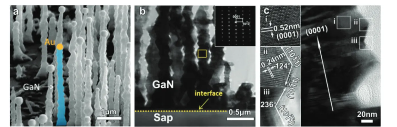
The direct epitaxy of GaN nanowires on the sapphire sub-strate at the NH3flux rate of 10 sccm and their good alignment allow us to further investigate the nucleation and growth mechanism. Typically, these GaN nanowires exhibit corrugated morphology and gold catalytic particles are found to terminate at the tip-end, as shown in Fig. 2a. The observation of Au nanoparticle catalysts suggests that the growth of the GaN
nanowires follows the vapor–liquid–solid (VLS) process.34 Ga adatoms decomposed from vaporized Ga2O3 powder will be directly adsorbed onto the melting Au droplets to form eutectic Au–Ga melt,35which serves as the catalyst to assist the GaN nanowire growth. The diffusion and dissolution of NH3 gas into the Au–Ga melts will lead to the supersaturation of the catalytic droplets. Notably, a low NH3 flowing rate, as employed in Fig. 1j and k, will provide a relative stable gas flow field around the vicinity of the substrate surface, and thus the supersaturated catalytic droplets are in good contact with the sapphire surface. In this way, the GaN nuclei would crystal-lize from the supersaturated catalytic Au–Ga melts at the liquid–solid interface and maintain a favorable epitaxial relationship, which will confine the growth of GaN along the crystalline orientation of the underlying sapphire substrate and eventually evolve into nanowires with uniform alignment, as schematically described in Fig. S3.† In addition, the absence of GaN nanowires in the region without the Au cata-lyst further demonstrates the VLS growth process, as shown in Fig. S4.† Unlike the smooth side surface of GaN nanorods,36 the GaN nanowires synthesized in this work exhibit a corru-gated appearance, which is composed of periodic concave and convex crystalline planes, as clearly observed in the SEM image and TEM image (Fig. 2a–c). The same morphology has once been observed in GaN nanorods grown on a graphite substrate in our previous work37and it is assumed that the formation of such corrugated morphology can be regarded as a combined effort of both the oscillation in nanowires’ radial growth38and the competing result of electrostatic interaction energy in the concave and convex planes.
Considering the crucial importance of growth temperature in nanowire synthesis, the influence of temperature on the growth of GaN nanowires is also investigated. It has been reported that the growth temperature influences the gas phase diffusion and substrate surface diffusion motilities.39The Ga adatom desorption rate on the substrate surface would be accelerated by increasing the substrate temperature, thus the nucleation process would be suppressed and the GaN
nano-Fig. 2 (a) Tilted SEM image and (b) low magnification cross-sectional TEM image of GaN nanowires epitaxially grown on sapphire; (inset is the corresponding SAED pattern obtained from the selected area of an individual nanowire labelled by a yellow box); (c) high-resolution TEM images of the GaN nanowires obtained from three different areas marked with i, ii and iii, respectively.
wire density reduces.40A similar tendency in nanowire density reduction has been observed when the growth temperature increases to above 1150 °C (Fig. S5†). Surprisingly, the increase of growth temperature has less impact on the alignment of the as-obtained GaN nanowire arrays. We assume the reason is the short transport distance of the reactive adatoms from the Ga2O3 precursors to the substrate surface, as illustrated in Fig. S1.†
The detailed morphology and crystal structure of the verti-cally-aligned GaN nanowire arrays are further analyzed with the help of TEM. Fig. 2b shows the low-magnification cross-sectional TEM image and we can confirm again the vertical standing of GaN nanowires with a rough and corrugated surface. In addition, we did not find an apparent interlayer between the GaN nanowires and sapphire substrate, implying the epitaxial nucleation and growth of GaN nanowires on the sapphire substrate at a lower NH3 flux rate of 10 sccm. The selective area electron diffraction (SAED) pattern obtained along the [121ˉ0] zone axis of the selected area (yellow box) of the representative GaN nanowire arrays (inset in Fig. 2b) exhi-bits succinct diffraction spots, demonstrating their single-crys-talline nature. From the corresponding high-resolution bright-field TEM image shown in Fig. 2c, one can see that the measured interplanar spacing of the lattice planes along the long-axis direction is 0.52 nm (Fig. 2c-i), corresponding to the (0001) plane and indicating the c-axis oriented growth of GaN nanowires. A representative protruded edge from an individual GaN nanowire is also selected to measure the side facets (Fig. 2c-ii). As can be seen, the interplanar spacing of the lattice plane parallel to the side surface is 0.24 nm, which is in good accordance with the {101ˉ1} plane of GaN. The angle between the neighboring crystalline facets is roughly measured to be 124°, which is consistent with the intersection angle between {101ˉ1} and {101ˉ1ˉ} lattice planes (Fig. S6†). Therefore, the periodic parallel side facets can be confidently identified as {101ˉ1} and {101ˉ1ˉ} planes. The angle between the lattice planes in Fig. 2c-iii is also in agreement with this speculation.
It is assumed that the corrugated morphology is complied with the Helmholtz principle41of minimum energy dissipa-tion, where the nanowires are enclosed by Ga3+-terminated (101ˉ1) and N3-terminated (101ˉ1ˉ) polar surfaces to maintain the minimization of the energy of the system.37,42Initially, the Ga and N atoms are arranged in the c-plane of WZ-GaN with a favorite hexagonal shape, followed by the atoms repeatedly de-posited on the previously formed GaN layer. Clearly, the depo-sition rate of the GaN layer along the c-axis direction is much faster than that on the two (101ˉ1) or (101ˉ1ˉ) sidewalls, leading to the formation of a one-dimensional morphology. The polar charges on the polar {101ˉ1} or {101ˉ1ˉ} sidewalls cause electro-static interaction energy which gradually decreases from layer to layer in a truncated hexagonal cone. When it reaches a certain point where the electrostatic surface energy makes the system unstable, opposite charged {101ˉ1ˉ} or {101ˉ1} sidewalls are thus formed to keep the overall energy preferentially stable. In this way, the formation of corrugated GaN nanowires is finally realized through the alternation of positive and
nega-tive charges on {101ˉ1} and {101ˉ1ˉ} sidewalls, as schematically illustrated in Fig. S3.† It is worth noting that the catalytic liquid droplet is on the nanoscale, so the size effect of the cata-lytic droplet is also considered.38The pressure differences in the catalytic droplet and the vapor have a significant influence on the growth kinetics. The pressure follows the Young– Laplace equation:43
Pin¼ Poutþ 2γl–v=R
where Pin is the pressure inside the catalytic liquid droplet, Pout is the pressure outside the droplet, γ(l–v) is the surface tension at the liquid–vapour interface, and R is the radius of the liquid catalytic droplet. The equation implies that when the droplet is on the nanometer scale and the growth system is under a specific pressure, the oscillation of R will lead to a strong oscillation in Pin. In the present VLS growth system at a temperature T and a pressure Pout, there should be a point where the vapor and liquid phases are in equilibrium. At this point, the chemical potential of the droplet with the equili-brium Re must be the same as the chemical potential of the vapor. However, the actual chemical potential of the droplet would be far away from equilibrium during the growth, so the droplet would approach the equilibrium chemical potential by adjusting R. If the chemical potential of the droplet is higher than that of the vapor, the droplet will continuously evaporate, and is accompanied by a diameter increase. Eventually, the evaporation will lead to an overshot to where the chemical potential of the droplet is lower than that of the vapor. So the droplet will absorb more vapor to increase its chemical poten-tial. This periodic oscillation process will lead to the radius (r) oscillation of the nanowire, which is linked with R due to the surface tension balance in the system following R = r sinθ, resulting in periodic oscillation in the nanowires’ radial growth. Similar morphologies are commonly seen in other hex-agonal structures.44
To disclose the atomic arrangement at the GaN/sapphire interface and further understand the nucleation mechanism, cross-sectional high-resolution TEM is utilized to determine the exact epitaxial relationship between the crystalline GaN nanowires and sapphire substrate. Fig. 3a shows a cross-sec-tional HRTEM image in the interfacial region. The atomically sharp interface between GaN and sapphire crystal domains suggests a direct epitaxial nucleation of GaN without the inser-tion of any buffering layer, distinctively different from the deposition process of GaN at a higher NH3flux rate. The inter-planar spacing of the lattice plane orthogonal to the substrate surface is measured to be 0.276 nm, which is in accordance with the (101ˉ0) plane of WZ-GaN. The corresponding lattice plane in the sapphire substrate parallel to the GaN (101ˉ0) plane is (112ˉ0) with an interplanar spacing value of 0.237 nm. Correspondingly, the c-planes in GaN and sapphire are parallel with each other and their lattice distances are in good agree-ment with their bulk crystals. The SAED pattern recorded at the interface marked with a white rectangular box in Fig. 3a further reflects the epitaxial relationship (Fig. 3b). According to the reciprocal lattice constants of WZ-GaN and the sapphire
crystal given in Fig. 3c, the epitaxial relationship between the GaN nanowire and the sapphire substrate can be further defined as (0001)GaN∥(0001)sapphire and (101ˉ0)GaN∥ (112ˉ0)sapphire, as experimentally verified in HRTEM observation (Fig. 3a). To meet the epitaxial requirement, the in-plane hexa-gonal unit cell of GaN should rotate 30° with respect to the [0001]-oriented sapphire substrate, as plotted in Fig. 3d. Without rotation, the lattice constant mismatch between GaN (101ˉ0) and sapphire (101ˉ0) can be up to 49.24%, which makes it impossible for the epitaxial growth. When the GaN unit cell is rotated by 30°, the GaN (101ˉ0) plane becomes parallel to the sapphire (112ˉ0) plane, and in this case the lattice constant mismatch can be significantly reduced to 13.87%,45which is still much higher for the heteroepitaxial nucleation of GaN. Such large lattice constant mismatching will result in a large structural strain and lead to the crack of the GaN film. To release the structural strain, misfit dislocation is observed at the GaN/sapphire interface. As is shown in the Fourier-filtered TEM (FFTEM) image in Fig. 3e, the nanowire/substrate inter-face displays misfit dislocations every seven fringes of the sapphire. The misfit dislocation periodicity is consistent with the 6 : 7 ratio of GaN/sapphire lattice planes, where every six lattice fringes in GaN (calculated domain width is 16.57 Å) is closely matched with every seven lattice fringes in sapphire
(calculated domain width is 16.65 Å) to produce a semi-coherent boundary at the interface.
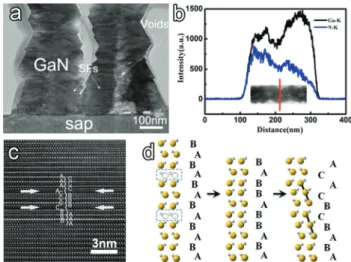
Stacking faults and voids have been reported in GaN nano-structures and heteronano-structures grown by catalytic-assisted methods. Low device efficiency is often related to high density of such structural imperfections.46,47 Fig. 4a shows a typical TEM image of the vertically oriented GaN nanowires contain-ing voids and stackcontain-ing faults. It is noteworthy that these voids are distributed along the axial direction within the nanowires. Generally, these voids have an inner diameter ranging from 70 to 100 nm, as convinced by the compositional profiles of N and Ga elements (Fig. 4b). It is assumed that the formations of these voids are generated by the different crystallization rates at the nanowire edge and center along the axial direction, as depicted in Fig. S3.† When Ga and N adatoms are absorbed at the solid–liquid (GaN/Au–Ga droplet) interface, the surface edge and center at the interface will crystallize simultaneously. However, if the crystallization rate at the edge (Ve) is faster than the rate in the center (Vc), it means that the outer part of the GaN nanowire will first evolve into a solid crystal, whereas the central part still maintains the liquid phase. When the central part crystallizes from liquid to solid, it will leave some continuous or discontinuous cavities due to the volume shrinking during the phase transition process, as observed in Fig. 4. If Veis close to Vc, the solid–liquid interface at GaN/Au– Ga will crystallize forward in a whole. In this case, there will be no voids formed, as seen in Fig. 4. It should be noted that the crystallization rates at the edge and center in the liquid–solid interface may be strongly dependent on the temperature fluc-tuation, gas flowing rate or local composition inhomogeneity, as validated by cathodoluminescence spectroscopy in GaN nanopyramids.36This assumption can be further supported by the GaN nanotubes prepared at a large NH3 flowing rate.48 Besides voids, stacking faults (SFs) featured as dark contrast
Fig. 3 (a) Atomically-scaled cross-sectional HRTEM image and (b) the corresponding SAED pattern obtained at the nanowire/substrate inter-face; (c, d) cross-sectional and in-plane lattice matching of epitaxial [0001]-oriented GaN on the [0001]-oriented sapphire substrate; (e) Fourier-filtered TEM image obtained from the FFT spot corresponding to the (101¯0) plane showing the misfit dislocation periodicity.
Fig. 4 (a) Representative TEM image of the vertically aligned GaN nanowires containing voids and SFs; (b) line-scan profiles of N and Ga elements taken along the radial direction; (c) HRTEM image of selected area with stacking faults and (d) the atomic illustration of the type I stacking fault formation.
stripes are clearly observed along the radial direction, two of which are marked by white arrows in Fig. 4a. It can be observed that the SFs are orthogonal to the growth direction of the nanowires, penetrating throughout the entire diameter. To further investigate the possible formation of SF, a HRTEM image of the nanowire is obtained along the [21ˉ1ˉ0] zone axis to observe and distinguish the stacking sequences (Fig. 4c). The perfect stacking sequence ABABAB in the WZ-GaN struc-ture is broken in the defective area by the alternation of the stacking sequence to ABABC̲BC̲A̲CA̲. It is thus identified to be the type I SF, which involves one breach of the WZ stacking rule where the third-nearest neighbor should be the same.49 Fig. 4d illustrates the formation of the type I SF in the WZ structure lattice. It is assumed that the formation of layer vacancies will directly lead to the generation of type I SFs with the lowest formation energy.50 Such SFs have been often observed in wurtzite-type GaN and ZnS nanowires or nano-belts32,51 and the temperature fluctuation/gradient is usually considered as the main reason for their formation.52
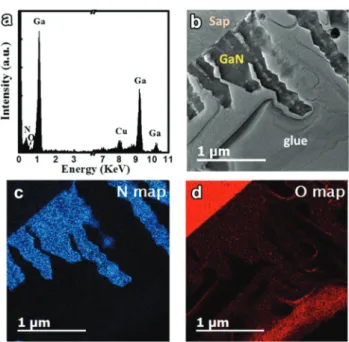
In the CVD synthesis process, gallium oxide powder is employed as the Ga source, which holds the possibilities of oxygen contamination in GaN nanowires. In addition, Van Nostrand et al. also claimed that the oxygen from the sapphire creates unintentional oxygen doping during GaN growth, raising its background electron concentration.53Therefore, it is essential to clarify the compositional purity of the as-syn-thesized nanowires. The quantitative analysis using EDS is per-formed on an individual GaN nanowire and we can only observe the predominant peaks from Ga, N and Cu (Cu signal comes from copper grids) elements (Fig. 5a). Ga and N elements have a uniform distribution inside the GaN
nano-wires, as verified by the elemental mapping and line-scan pro-files (Fig. S7†). The weak O peak shoulder near the N peak in the EDS spectrum can be hardly observed. To further confirm the oxygen doping in GaN nanowires, energy filtered trans-mission electron microscopy (EFTEM) with much higher com-positional resolution is then employed to examine the trace amount of O element from the GaN nanowires vertically grown on the sapphire substrate. Fig. 5b–d depict the typical zero-loss image of GaN nanowires on the sapphire substrate and its corresponding EFTEM micrographs of N (from the K edge peak at 401 eV) and O (from the K-edge peak at 532 eV) elements. The mapping of the N element in Fig. 5c matches well with the configuration of GaN nanowires, suggesting the uniform distribution of the N element inside the GaN nano-wires. On the contrary, the mapping of the O element in Fig. 5d shows a predominant intensity in the sapphire sub-strate side and a very weak intensity in the GaN nanowire arrays, suggesting low contamination of oxygen in the GaN nanowire host. This is in agreement with the EDS spectrum in which the O related peak is hardly visible.
As a key III–V group nitride semiconductor, GaN has perva-sive applications and technological importance in building high-performance optoelectronics due to its outstanding luminescence properties and the direct wide band-gap of 3.4 eV.54–56 The evaluation of luminescence emissions of GaN nanowires is extremely crucial for their integration into opto-electronic nanodevices. Fig. 6 shows the PL spectrum of GaN nanowire arrays epitaxially grown on the sapphire substrate under the excitation of a 325 nm He–Cd laser. It can be seen that the GaN nanowires exhibit a dominant peak centered at 385 nm wavelength and a broad visible band in the scanning range from 330–700 nm. The 385 nm peak could be assigned to the near band-edge emission (NBE) and has been observed in various GaN nanostructures.57The value (41 nm) of the full width at half maximum (FWHM) is much larger than that of the GaN nanowires grown on buffering and barrier layers, which has a FWHM value of 17 nm.31The large FWHM value may originate from the structural strain and SFs due to the large lattice mismatching and further implies the degraded
Fig. 5 (a) EDS spectrum obtained from a randomly selected individual GaN nanowire; (b) the typical zero-loss EFTEM image and its chemical mappings of (c) N (from the K edge at 401 eV) and (d) O (from the K edge at 532 eV) elements.
Fig. 6 Room-temperature photoluminescence spectrum of GaN nano-wires epitaxially grown on a sapphire substrate under the excitation of a 325 nm He–Cd laser.
crystal quality. Occasionally, the dislocation from the under-lying sapphire substrate can also be observed to thread the interface and penetrate into the GaN crystal, leading to the broadening of the NBE emission.58The weak dome peaked at 593 nm wavelength in the visible range of 500–700 nm can be assigned to the yellow luminescence (YL) emission, which is also widely observed in various GaN crystals.59,60This YL emis-sion is widely accepted as a defect-related luminescence and is generally considered to be a key parameter to evaluate the optical performance of the GaN crystal. A higher intensity of the YL emission implies a poorer crystal quality and possible impurity contamination. Our previous work also demonstrated that the insertion of buffering and barrier layers can effectively depress the YL emission through the isolation of threading dislocations from the substrate.31In the current work, this YL band may come from the negligible oxygen contamination and the structural defects instead of threading dislocations since we did not observe these defects from TEM analysis. The luminescence properties of GaN nanowire arrays can be further improved through the homoepitaxy of GaN nanowires on the GaN substrate without lattice and thermal mismatching or the adoption of suitable buffering/barrier layers.61,62 For instance, Hao and Heilmann et al. utilized atomically thin gra-phene or BN layers for the realization of high-quality GaN crys-tals.63,64In this way, the integration of various high-perform-ance and high-efficiency optoelectronic nanodevices based on high-quality GaN nanowire arrays can be expected and the current work paves a solid way toward the development of GaN-based nanomaterials and nanotechnology.
Conclusions
In summary, GaN nanowires with uniform alignment along the [0001] direction have been obtained in a simple Au-assisted CVD process. The alignment homogeneity of the GaN nanowires is further realized through the control of NH3gas at a low flowing rate. The lower NH3 flowing rate enables the homogeneous nucleation of GaN on the sapphire substrate to establish the direct epitaxial relationship and the GaN growth direction can be well confined by the underlying sapphire sub-strate. HRTEM analysis reveals the formation of hollow cavities and the generation of stacking faults inside the GaN nano-wires. Additionally, a periodic misfit dislocation is also observed to release the structural strain due to the large lattice constant mismatch between GaN and sapphire. Accurate com-position analysis using EFTEM imaging finds low oxygen con-tamination in the GaN lattice host. Optical characterization of the GaN nanowires reveals that the nanowire arrays exhibit a sharp NBE emission band in the UV range and a weak dome in the visible range, demonstrating the decent luminescence properties of GaN nanowires. The finding in this work not only elucidates the key factor governing the alignment control of GaN nanowires on the sapphire substrate, but also further discloses the lattice matching in the GaN/sapphire interface on the atomic scale using HRTEM. Obtaining highly aligned
GaN nanowires will further promote their technologically important applications in the heteroepitaxial growth of GaN crystals, highly bright nano-LEDs, photovoltaic cells, photo-detectors and other related optoelectronic nanodevices.
Con
flict of interest
The authors declare no competing financial interest.
Acknowledgements
This work was mainly supported by the Knowledge Innovation Program of Institute of Metal Research, Chinese Academy of Sciences with grant no. Y2NCA111A1 and Y3NCA111A1, and the Youth Innovation Promotion Association, Chinese Academy of Sciences (grant no. Y4NC711171). Xavier Portier and Christophe Labbé would like to thank Marie Pierre Chauvat for her expertise in using the FIB system for the TEM sample and also the French ANR (Agence Nationale de la Recherche) institution for the EQUIPEX“GENESIS” grant that allowed the acquisition and the use of the FIB system (HELIOS
Nanolab 600 from FEI) and the EELS spectrometer
(QUANTUM ER965 from GATAN).
References
1 A. I. Hochbaum and P. Yang, Chem. Rev., 2009,110, 527– 546.
2 K. Tomioka, F. Izhizaka and T. Fukui, Nano Lett., 2015,15, 7253–7257.
3 K. Nagashima, T. Yanagida, K. Oka, M. Taniguchi, T. Kawai, J.-S. Kim and B. H. Park, Nano Lett., 2010, 10, 1359–1363.
4 E. Garnett and P. Yang, Nano Lett., 2010,10, 1082–1087.
5 S. W. Boettcher, J. M. Spurgeon, M. C. Putnam,
E. L. Warren, D. B. Turner-Evans, M. D. Kelzenberg, J. R. Maiolo, H. A. Atwater and N. S. Lewis, Science, 2010, 327, 185–187.
6 X. Zhang, Y. Liu and Z. Kang, ACS Appl. Mater. Interfaces, 2014,6, 4480–4489.
7 Y. Huang, X. F. Duan, Q. Q. Wei and C. M. Lieber, Science, 2001,291, 630–633.
8 A. V. Akimov, J. T. Muckerman and O. V. Prezhdo, J. Am. Chem. Soc., 2013,135, 8682–8691.
9 B. O. Jung, S.-Y. Bae, S. Y. Kim, S. Lee, J. Y. Lee, D.-S. Lee, Y. Kato, Y. Honda and H. Amano, Nano Energy, 2015, 11, 294–303.
10 Z. Yan, G. Liu, J. M. Khan and A. A. Balandin, Nat. Commun., 2012,3, 827.
11 C.-Y. Chen, G. Zhu, Y. Hu, J.-W. Yu, J. Song, K.-Y. Cheng, L.-H. Peng, L.-J. Chou and Z. L. Wang, ACS Nano, 2012,6, 5687–5692.
12 Y. B. Tang, X. H. Bo, C. S. Lee, H. T. Cong, H. M. Cheng, Z. H. Chen, W. J. Zhang, I. Bello and S. T. Lee, Adv. Funct. Mater., 2008,18, 3515–3522.
13 X. B. Wang, J. H. Song, F. Zhang, C. Y. He, Z. Hu and Z. L. Wang, Adv. Mater., 2010,22, 2155–2158.
14 P. Deb, H. Kim, Y. Qin, R. Lahiji, M. Oliver, R. Reifenberger and T. Sands, Nano Lett., 2006,6, 2893–2898.
15 R. Koester, D. Sager, W.-A. Quitsch, O. Pfingsten, A. Poloczek, S. Blumenthal, G. Keller, W. Prost, G. Bacher and F.-J. Tegude, Nano Lett., 2015,15, 2318–2323.
16 T. R. Kuykendall, M. V. Altoe, D. F. Ogletree and S. Aloni, Nano Lett., 2014,14(12), 6767–6773.
17 A. H. Chin, T. S. Ahn, H. Li, S. Vaddiraju, C. J. Bardeen, C. Z. Ning and M. K. Sunkara, Nano Lett., 2007,7, 626–631. 18 T. Kuykendall, P. J. Pauzauskie, Y. F. Zhang, J. Goldberger,
D. Sirbuly, J. Denlinger and P. D. Yang, Nat. Mater., 2004,3, 524–528.
19 Y. Sun, Y.-H. Cho, H.-M. Kim and T. W. Kang, Appl. Phys. Lett., 2005,87, 093115.
20 S. D. Hersee, X. Sun and X. Wang, Nano Lett., 2006, 6, 1808–1811.
21 J. Zhang, L. D. Zhang, X. F. Wang, C. H. Liang, X. S. Peng and Y. W. Wang, J. Chem. Phys., 2001,115, 5714–5717. 22 S. Fernández-Garrido, V. M. Kaganer, K. K. Sabelfeld,
T. Gotschke, J. Grandal, E. Calleja, L. Geelhaar and O. Brandt, Nano Lett., 2013,13, 3274–3280.
23 V. M. Kaganer, S. Fernández-Garrido, P. Dogan,
K. K. Sabelfeld and O. Brandt, Nano Lett., 2016, 16(6), 3717–3725.
24 F. Schuster, M. Hetzl, S. Weiszer, J. A. Garrido, M. de la Mata, C. Magen, J. Arbiol and M. Stutzmann, Nano Lett., 2015,15(3), 1773–1779.
25 C. G. Tu, C. Y. Su, C. H. Liao, C. Hsieh, Y. F. Yao, H. T. Chen, C. H. Lin, C. M. Weng, Y. W. Kiang and C. C. Yang, Nanotechnology, 2016,27, 025303.
26 P. M. Coulon, B. Alloing, V. Brandli, D. Lefebvre, S. Chenot and J. Zuniga-Perez, Phys. Status Solidi B, 2015,252, 1096– 1103.
27 Q. M. Li, Y. Lin, J. R. Creighton, J. J. Figiel and G. T. Wang, Adv. Mater., 2009,21, 2416–2420.
28 C. T. Huang, J. Song, W. F. Lee, Y. Ding, Z. Gao, Y. Hao, L. J. Chen and Z. L. Wang, J. Am. Chem. Soc., 2010,132, 4766–4771.
29 Z. Wu, M. G. Hahm, Y. J. Jung and L. Menon, J. Mater. Chem., 2009,19, 463–467.
30 B. D. Liu, Z. E. Wang, F. Yuan, D. Benjamin, T. Sekiguchi and X. Jiang, RSC Adv., 2013,3, 22914–22917.
31 B. D. Liu, F. Yuan, B. Dierre, T. Sekiguchi, S. Zhang, Y. K. Xu and X. Jiang, ACS Appl. Mater. Interfaces, 2014,6, 14159–14166.
32 B. D. Liu, Y. Bando, M. S. Wang and D. Golberg, J. Nanosci. Nanotechnol., 2010,10, 3945–3951.
33 B. D. Liu, Y. Bando, C. C. Tang, F. F. Xu and D. Golberg, Appl. Phys. Lett., 2005,87, 073106.
34 R. S. Wagner and W. C. Ellis, Appl. Phys. Lett., 1964,4, 89– 90.
35 R. E. Diaz, R. Sharma, K. Jarvis, Q. Zhang and S. Mahajan, J. Cryst. Growth, 2012,341, 1–6.
36 B. Liu, Z. Wang, F. Yuan, D. Benjamin, T. Sekiguchi and X. Jiang, RSC Adv., 2013,3, 22914.
37 F. Yuan, B. D. Liu, Z. E. Wang, B. Yang, Y. Yin, B. Dierre, T. Sekiguchi, G. F. Zhang and X. Jiang, ACS Appl. Mater. Interfaces, 2013,5, 12066–12072.
38 H. Wang, J. T. Wang, Z. X. Cao, W. J. Zhang, C. S. Lee, S. T. Lee and X. H. Zhang, Nat. Commun., 2015, 6, 6412.
39 S. Chae, K. Lee, J. Jang, D. Min, J. Kim and O. Nam, J. Cryst. Growth, 2015,409, 65–70.
40 S. Zhao, M. G. Kibria, Q. Wang, H. P. T. Nguyen and Z. Mi, Nanoscale, 2013,5, 5283–5287.
41 D. G. Christopherson and D. Dowson, Proc. R. Soc. A, 1959, 251, 550–564.
42 X. Xie, G. Z. Wang, Z. B. Shao and D. P. Li, J. Phys. Chem. C, 2009,113, 14633–14637.
43 F. L. Román, J. Faro and S. Velasco, Am. J. Phys., 2001,69, 920–921.
44 R. Yang, Y. Ding and Z. L. Wang, Nano Lett., 2004,4, 1309– 1312.
45 L. Liu and J. H. Edgar, Mater. Sci. Eng., R, 2002, 37, 61–127.
46 D. Tham, C. Y. Nam and J. E. Fischer, Adv. Funct. Mater., 2006,16, 1197–1202.
47 Y.-D. Lin, A. Chakraborty, S. Brinkley, H. C. Kuo, T. Melo, K. Fujito, J. S. Speck, S. P. DenBaars and S. Nakamura, Appl. Phys. Lett., 2009,94, 261108.
48 B. D. Liu, Y. Bando, C. C. Tang, G. Z. Shen, D. Golberg and F. F. Xu, Appl. Phys. Lett., 2006,88, 093120.
49 B. Yang, B. Liu, Y. Wang, H. Zhuang, Q. Liu, F. Yuan and X. Jiang, Nanoscale, 2015,7, 16237–16245.
50 B. D. Liu, B. Yang, B. Dierre, T. Sekiguchi and X. Jiang, Nanoscale, 2014,6, 12414–12420.
51 J. Lahnemann, U. Jahn, O. Brandt, T. Flissikowski, P. Dogan and H. T. Grahn, J. Phys. D: Appl. Phys., 2014,47, 423001.
52 F. Meng, M. Estruga, A. Forticaux, S. A. Morin, Q. Wu, Z. Hu and S. Jin, ACS Nano, 2013,7, 11369–11378.
53 J. E. Van Nostrand, J. Solomon, A. Saxler, Q. H. Xie, D. C. Reynolds and D. C. Look, J. Appl. Phys., 2000, 87, 8766.
54 I. Akasaki, Angew. Chem., Int. Ed., 2015, 54, 7750– 7763.
55 H. Amano, Angew. Chem., Int. Ed., 2015,54, 7764–7769. 56 S. Nakamura, Angew. Chem., Int. Ed., 2015,54, 7770–7788. 57 B. Liu, L. Hu, C. Tang, L. Liu, S. Li and J. Qi, Mater. Sci.
Eng., B, 2011,176, 805–809.
58 Y. S. Chen, W. Y. Shiao, T. Y. Tang, W. M. Chang, C. H. Liao, C. H. Lin, K. C. Shen, C. C. Yang, M. C. Hsu, J. H. Yeh and T. C. Hsu, J. Appl. Phys., 2009, 106, 023521.
59 T. Suski, P. Perlin, H. Teisseyre, M. Leszczyński, I. Grzegory, J. Jun, M. Boćkowski, S. Porowski and T. D. Moustakas, Appl. Phys. Lett., 1995,67, 2188–2190.
60 S. Xu, Y. Hao, J. Zhang, T. Jiang, L. Yang, X. Lu and Z. Lin, Nano Lett., 2013,13, 3654–3657.
61 C. Wetzel, M. Zhu, J. Senawiratne, T. Detchprohm, P. D. Persans, L. Liu, E. A. Preble and D. Hanser, J. Cryst. Growth, 2008,310, 3987–3991.
62 H. Amano, I. Akasaki, K. Hiramatsu, N. Koide and N. Sawaki, Thin Solid Films, 1988,163, 415–420.
63 L. Zhang, X. Li, Y. Shao, J. Yu, Y. Wu, X. Hao, Z. Yin, Y. Dai, Y. Tian, Q. Huo, Y. Shen, Z. Hua and B. Zhang, ACS Appl. Mater. Interfaces, 2015,7, 4504–4510.
64 M. Heilmann, A. M. Munshi, G. Sarau, M. Goebelt, C. Tessarek, V. T. Fauske, A. T. J. van Helvoort, J. Yang, M. Latzel, B. Hoffmann, G. Conibeer, H. Weman and S. Christiansen, Nano Lett., 2016,16, 3524–3532.