HAL Id: hal-00485716
https://hal.archives-ouvertes.fr/hal-00485716
Submitted on 19 Apr 2021
HAL is a multi-disciplinary open access
L’archive ouverte pluridisciplinaire HAL, est
An acoustic waveguide based on doubly-bonded
silicon/PPT/silicon structures
E. Courjon, F. Bassignot, G. Ulliac, Thierry Laroche, J. Garcia, D. Gachon,
S. Queste, J.-P. Romand, S. Ballandras, R. Petit
To cite this version:
E. Courjon, F. Bassignot, G. Ulliac, Thierry Laroche, J. Garcia, et al.. An acoustic waveguide based
on doubly-bonded silicon/PPT/silicon structures. 22nd IEEE International European Frequency and
Time forum, Apr 2009, Besançon, France. pp.898-903, �10.1109/FREQ.2009.5168317�. �hal-00485716�
An acoustic waveguide based on doubly-bonded
silicon/PPT/silicon structures
E. Courjon, F. Bassignot, G. Ulliac, T. Laroche, J.
Garcia, D. Gachon, S. Queste, J-P. Romand, S.
Ballandras
Institut FEMTO-STUMR 6174 CNRS-UFC-ENSMM-UTBM 26 che. de l'épitaphe, 25000 Besançon, France
R. Petit
CELAR DGA Rennes, FranceAbstract—In this paper, we present new results on the
development of piezoelectric transducers based on periodically poled ferroelectric domains in a lithium niobate plate bonded between two silicon wafers. The fabrication of the periodically poled transducers operating in the range 50 – 500 MHz has been achieved on a 3 inches 500 μm thick wafer. These devices then have been bonded on silicon wafers to fabricate a waveguide. Guided elliptic as well as partially guided longitudinal modes are excited. The experimental responses of the tested devices are compared to predicted harmonic admittances, showing a good agreement between both results and allowing for a reliable analysis of the nature of the excited modes. We also show interesting studies of material combinations used to guide ultrasonic waves. Dispersion properties have also been studied for a structure Si/PPT/Si.
I. INTRODUCTION
Periodically Poled Transducers (PPTs) have been investigated recently as an alternative to classical inter-digital transducers for the excitation and detection of guided acoustic waves. The structure simply consists of two electrically conductive media deposited on each side of a periodically poled ferroelectric layer. This structure has been implemented using Z-cut of LiNbO3 [1] and has been associated with silicon
to manufacture waveguides for radio-frequency (RF) applications. The excitation and detection principle suppresses the need for zero-defect lithography processes as the domain poling is not prevented by partially resolved resist lines and finally the top electrodes does not require any periodical structuring. However, this solution still shares with standard Surface Acoustic Wave (SAW) devices the need for packaging preventing any surface pollution which may here simply degrade the wave propagation (the electrical excitation actually is robust to surface pollution by principle). The best solution to allow for applying low cost packaging techniques to acoustic-wave-based devices consists of exciting waves trapped within a guiding structure in the bulk of implemented materials. This gives rise to the concept of Interfacial or Boundary Acoustic
Waves. Many groups have been investigating the possibility to develop such solutions using standard inter-digited transducers. They must overcome the difficulty of processing machined surfaces, loosing the flatness qualities generally used for wafer bounding techniques. They may also used thick layer deposition approaches, then loosing the interest of single crystals, still the best solution for high quality factor acoustic wave resonators.
In this work, we have considered the possibility to combine the wave guiding within the bulk with our periodically poled transducers to benefit of all the pointed advantages of both approaches. First of all, we explain the periodically poled transducers fabrication principle and we present experimental results on lithium niobate (LiNbO3) and lithium tantalate
(LiTaO3) wafers. After that, we present theoretical analysis
results achieved using our finite element/boundary element simulation tool, allowing for the simulation of such material combinations used to guide ultrasonic waves. We have pointed out the existence of elliptically polarized guided modes for several material combinations and technological parameters. We also have identified the possibility to excite partially guided longitudinally polarized waves. theoretical analysis results of the PPT operation obtained, using our finite and boundary element simulation tool. Using the analysis of the transducer dispersion properties providing the optimum operating points and the temperature coefficient of frequency (TCF) analysis, we have chosen the best combination Si/PPT/Si to fabricate test vehicles. Poled LiNbO3 wafers are
first bonded onto silicon using Au/Au compression, then the resulting stack is metalized again to process a second wafer bonding on silicon as previously. These devices did exhibit a period of 50 μm (domain width 25 μm), yielding operating frequencies near 80 MHz. As predicted, we measure both contributions of elliptic and longitudinal modes near the expected contributions.
II. ADVANTAGES, FABRICATION AND CHARACTERIZATION OF PERIODICALLY POLED TRANSDUCERS
A. Advantages
PPTs have two principal advantages compared to standard periodic inter-digital electrode transducer (IDTs) deposited atop piezoelectric materials. The first one is the robustness of the excitation versus defects or surface contamination (no passivation is required to avoid short circuit as in the case of standard IDTs) and the second one is the possibility to excite waves exhibiting a wavelength equal to the poling period, contrary to standard IDTs for which the wavelength is twice the mechanical period of the grating (Bragg condition). It can also be noted that comparably to film bulk acoustic resonators (FBARs), it can operate with large excitation powers as the electrodes are separated by a bulk material layer. We have shown in [2] the capability of the structure to excite elliptically and longitudinally polarized plate waves (Lamb modes). The PPT is fundamentally based on a periodically poled piezoelectric medium. Each side of this medium is metalized in order to obtain a capacitive dipole in which elastic waves can be excited by phase construction. Such a periodically poled structure can be advantageously achieved on ferroelectric materials like PZT because of the rather small value of its coercive electric field (the absolute value of the electric field above which the spontaneous polarization can be inverted) or LiNbO3 and LiTaO3.
B. Fabrication
As previously presented [1,2], we have performed our experiments on a dedicated poling bench which can control the poling of thick (500 µm) optical quality Z-cut LiNbO3 plates. It
mainly consists of a high voltage amplifier used to submit the wafer to an electric field strong enough to invert the negative poling of the material. The coercive electric field of the lithium niobate is 21 kV/mm, consequently, the voltage needed to invert the domains is approximately 11 kV. The domains to be poled are defined using a photo-resist pattern on top of a plate surface. We have used a mask with several devices of 50 µm poling period. The plate is held in a Polymethyl methacrylate
(PMMA) mounting by means of two O-ring joints which create
two cavities full filled by a saturated lithium chloride solution used as a liquid electrode (as it is shown in the scheme of fig.1).
Figure 1. Principle of the domain inversion bench
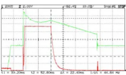
The high poling voltage is applied to the plate following the sequence shown in fig. 2. This sequence is designed to favor the domain nucleation, to stabilize the inverted domains (i.e. to avoid back-switching of the domains) and to avoid electrical breakdowns [3]. The poling process is monitored thanks to the measurement of the electric current crossing the wafer during the sequence. The signature of a successful domain inversion corresponds to a voltage dropping while a current discharge occurs simultaneously (see fig.2). The poling can be easily controlled by a simple optical post- observation, as it generates a contrast at the edge of the poled domains (see fig.3).
Figure 2. Domain inversion monitoring: probed high voltage applied on the wafer (green curve, poling sequence) and resulting crossing current (red curve). Voltage and current gain are respectively 1V/5000V and 1V/5mA. 1st
step : the applied electric field is smaller than the coercive limit, to prepare the sample for the nucleation step. 2nd
step : the applied field overcomes the coercive limit, yielding nucleation and consequently poling (this step lies between the 2 dashed cursors). 3rd
step : linear decrease of the field to end-up the nucleation (self-termination step, exponential decrease of
the current). 4th
step : stabilization of the poling by applying a field smaller than the coercive limit
Figure 3. Optical verification of the poling efficiency, case of a 50 µm period device, evidence of contrast changes between Z+ (native polarization) and Z– (switched polarization) domains. The evidence of contrast modification in the vicinity of the poled domain walls at the poled strip edge (the whole plate is Z+ oriented, the poled strips are Z– oriented)
may e due to diffusion effects
C. Experimental results compared with theoretical analysis
We demonstrate the concept validity (Si/PPT(p=50 µm)/Si) at about 80 MHz. To characterize periodically poled transducers, we metalized each side of the transducer (sides Z+ and Z-) with an aluminum layer. After that, the devices are characterized using a network analyzer. One side of the device is connected to the signal whereas the second one is linked to the ground. We obtain a response (fig. 4) with numerous
parasitic bulk wave residuals but two strong contributions are pointed out at 76 and 130 MHz respectively. We compare the experimental results with the theoretical analysis using our finite element/boundary element simulation tool. The first value can be easily related to the asymptotic limit emphasized for the very first Lamb wave contribution (i.e. Rayleigh wave velocity) and the second one approaches the longitudinal bulk wave velocity along X axis.
Figure 4. Theory/experiment admittance of the 50 µm period PPT device. Two strong waves are visible, respectively at 76 and 130 MHz
III. MODELING WAVEGUIDES USING PERIODICALLY POLED TRANSDUCERS
In this part, we first present analysis results achieved using our finite element/boundary element simulation tool [4], allowing for the simulation of such material combinations. After that, the combination of material Si/PPT/Si is chosen (easiest and cheapest to fabricate) and the dispersion properties of this transducer are studied providing the best operating points.
A. Analysis of several material combinations
The purpose of this analysis is to study influences on wave guidance and velocity. For that, we study two principal cases using LiNbO3 and LiTaO3 as ferroelectric material and we
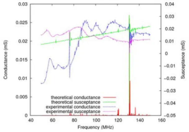
modify the guidance material (silicon, sapphire or diamond). Theoretical analysis results of these structures are obtained by means of our finite and boundary element simulation tool. Figures 5 and 6 show the theoretical admittance of LiNbO3 and
LiTaO3 PPT respectively (p=50 µm).
(a) (b)
Figure 5. (a) Scheme of the PPT structure (b) Theoretical admittance of a 50 µm period LiNbO3 PPT for 30 or 60 µm thick for different
guiding substrates
Figure 6. Theoretical admittance of a 50 µm period LiTaO3 PPT
for 30 or 60 µm thick for different guiding substrates
There are two main differences between LiNbO3 and LiTaO3
transducers. The first one is a better spectrum purity for the LiTaO3 configuration in comparison with the LiNbO3
configuration. The second one concerns the Rayleigh wave velocity of LiTaO3 (3500 m.s-1) which is lower than the one of
LiNbO3 (3800 m.s-1), that is why we observe the same acoustic
waves for both materials and for each guiding substrates but at a lower frequency for the LiTaO3. The guidance conditions
also depend on the ratio between the ferroelectric material thickness and the transducer wavelength (h/p). The elliptic mode actually is guided from a ratio h/p equal to 1. The structure diamond/PPT/diamond is the most guiding configuration thanks to the high propagation velocities in the diamond (12500 m.s-1 for the Surface Skimming Bulk Wave (SSBW)). In fact, the quasi-longitudinal mode is excited and guided at a velocity around 6500 m.s-1. The last structure consisting of a silicon/PPT/silicon stuck presents interesting guidance properties for a ratio (h/p) smaller than 1, this parameter is treated in the next part. In this structure, the
Guiding layer Guiding layer LiNbO3 transducer
elliptic mode is mainly excited at about 5100 m.s-1 whereas the longitudinal mode at about 7300 m.s-1 is not guided, as the SSBW velocity in the silicon is near 5800 m.s-1. This configuration is retained for the rest of the study because the elliptic mode is well guided, the fabrication process is quite simple and cheaper than structures based on other guiding materials.
B. Analysis of dispersion properties
We propose to closely investigate how to efficiently derive the dispersion curves and then to show at least for the elliptic mode of the waveguide the influence of the PPT geometry and the operating frequency on the mode properties. In that matter, we have considered the general shape of the transducer symbolized in fig.7. We assume here a propagation between two silicon layers but the approach can be generalized to any guiding substrate. The period is arbitrarily fixed to 10 µm (i.e. width of each LiNbO3 domain set to 5 µm, poling ratio=0.5).
Figure 7. Scheme of PPT principle and generic shape for dispersion curve derivation
In Figure 8, we have plotted the theoretical admittance (conductance and susceptance) versus frequency for a thickness/period (h/p) ratio equal to 0.1, in order to identify the main contribution corresponding to an elliptically shaped mode.
Figure 8. Harmonic admittance of the structure plotted in fig.7 for a thickness/period ratio equal to 0.1
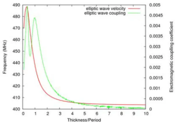
Once the mode identified, we follow the evolution of its resonance frequency and electromagnetic coupling coefficient for h/p ratios ranging from 0.1 to 10, is plotted on fig.9.
Figure 9. Evolution of the elliptic mode synchronism frequency (red curve) and electromagnetic coupling (green curve) for small values of
h/p ratio (ranging from 0.1 to 10 in our calculation)
There is no ambiguity concerning the elliptic polarization of the studied mode because there is no possible interaction with other modes (as often observed for Lamb waves for instance). This operating point is of very particular importance as it conditions the possibility to improve the design reliability by choosing operation condition poorly affected by technology, which is a key point for any practical exploitation of the device. The next section shows the fabrication of a device Si/PPT/Si.
IV. DOUBLE BONDING SI/PPT/SI : FABRICATION,
CHARACTERIZATION AND TEMPERATURE SENSIBILITY
The concept has been experimentally checked first using a thick structure consisting of a Silicon(380 µm thick)/LiNbO3
PPT (500 µm)/Silicon (380 µm) material stack.
A. Fabrication
The fabrication of PPT-based waveguides consists in bonding a silicon wafer on each side of the periodically poled wafer. In that purpose, the lithium niobate wafer is bonded on a (100) 3" silicon wafer using a wafer bonding technique developed in our group based on a metal-metal adhesion at room temperature promoted by a high pressure applied to the material stack (fig.10). Connection via are etched in each silicon substrate by Deep Reactive Ion Etching (DRIE) in order to reach the buried metallic electrodes. After that, the structure is diced to obtain 5 separated devices.
Figure 10. Double bonding of a lithium niobate wafer (center of the photograph) with silicon wafer (top and bottom) using room temperature
Au/Au bonding process
The process flowchart is reported in fig.11, showing the different implemented coatings and the technological sequence.
Figure 11. Flowchart which summarizes the different steps of realization of the device
A test vehicle is mounted on a metallic surface (printed circuit) to connect electrically the structure with the support and a SMA port is added to connect the support to a RF spectrum analyzer (fig.12).
Figure 12. Test vehicle of a Si/LiNbO3 PPT/Si device
B. Characterization and temperature sensibility
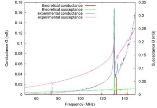
Figure 13 presents the comparison between the experimentally measured responses of the implemented devices and the theoretical harmonic admittances obtained with our periodic finite element code. Measurements have been achieved successfully for the 50 µm period devices, as explained above. Since the implemented single-port test devices are quite long and almost behave as single port resonators, the comparison between measurement and harmonic admittance results makes sense.
Figure 13. Comparison between the test vehicle admittance and the theoretical admittance
This plot points out the good agreement between both results. We find two main contributions corresponding to the elliptical mode and the longitudinal mode. We can notice that the experimental admittance increases gradually. The main cause seems to be the wire length of the connection between the device and the support. This proves the feasibility of LiNbO3
-based Silicon/PPT/Silicon devices.
1. Photoresist pattern
2. Poling
3. Photoresist removing
4. Bonding with a silicon wafer
5. Bonding with a 2nd silicon wafer
6. Etch silicon (DRIE) LiNbO3
Photoresist Domain inversion
Silicon Gold layer
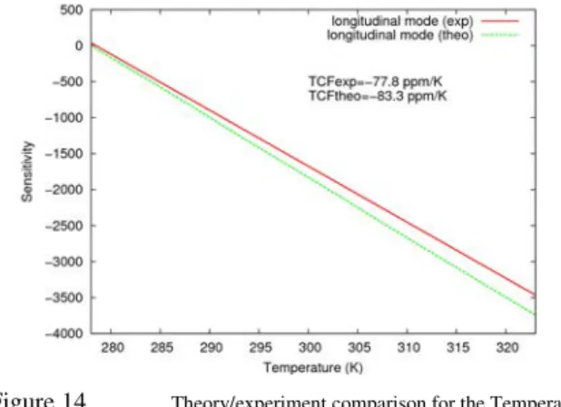
We also have measured the experimental admittance of the longitudinally polarized wave at different temperatures (between 278 and 323 K) of the test vehicle. Figure 14 shows the comparison between the theoretical and the experimental Temperature Coefficient of Frequency (TCF). We obtain the same order of magnitude at around -80 ppm/K. We can notice that the TCF is sensibly the same than the one of isolated LiNbO3 devices.
Figure 14. Theory/experiment comparison for the Temperature Coefficient of Frequency (TCF)
V. CONCLUSION
We have proposed a first analysis of waveguides using different material combinations. We can mainly notice that acoustic waves in a LiNbO3 structure are guided more rapidly
and with less spectrum purity than the ones in a LiTaO3
structure. An analysis concerning the dispersive behavior of PPT-based waveguide has been also achieved. These analysis are performed using FEA-BEM calculations as it is one of the only approach capable to accurately address this problem. We have demonstrated the feasibility of acoustic waveguide using periodically poled transducer on LiNbO3 Z-cut bonded
between two silicon wafers. The devices have been found to operate according to the theoretical predictions, allowing for a reliable analysis of their operation. The TCF of these devices is relatively high but a future work consisting in thinning the ferroelectric material will enable to reduce it considerably.
ACKNOWLEDGMENT
This work was supported by the french DGA (Délégation Générale pour l’Armement) under grant#07-34-020.
REFERENCES
[1] E. Courjon, J. Hauden, J. Masson, D. Gachon, L. Gauthier Manuel, W. Daniau, N. Bodin, S. Ballandras, “Pure longitudinal plate mode excited by poled domains transducers on LiNbO3”, Proc. of the IEEE IFCS,
2007
[2] E. Courjon, J. Hauden, P. Parruch, J. Masson, D. Gachon, L. Gauthier Manuel, W. Daniau, , N. Bodin, J.M. Triscone, S. Ballandras, “Fabrication of periodically poled domains transducers on LiNbO3”,
Proc. of the IEEE IFCS, Miami, 2006
[3] S. Ballandras, W. Daniau, B. Gautier, D. Hauden, M. Wilm, V. Laude, V. Ruch, S.Flambart, “A novel surface wave transducer based on periodically poled piezoelectric domain”, Proc of the IEEE IFCS, 2006 [4] S. Ballandras, R. Lardat, M. Wilm, Th. Pastureaud, A. Reinhardt, N.
Champavert, W. Steichen, W. Daniau, V. Laude, R. Armati, G. Martin, “A mixed finite element/boundary element approach to simulate complex guided elastic wave periodic transducers”, accepted for publication in Journal of Applied Physics, 2008