Critical Temperatures of Superconducting Solders
by
Erica Medeiros Pav&o
SUBMITTED TO THE DEPARTMENT OF MECHANICAL ENGINEERING IN PARTIAL FULFILLMENT OF THE REQUIREMENTS FOR THE DEGREE OF
BACHELOR OF SCIENCE AT THE
MASSACHUSETTS INSTITUTE OF TECHNOLOGY
JUNE 2007
02007 Erica Medeiros Pavio All rights reserved.
The author hereby grants to MIT permission to reproduce and to distribute publicly paper and electronic copies of this thesis document in whole or in part in
any medium now known or hereafter created.
Signature of Author: Certified by: Accepted by:_ MASSACHUSETTS INSTI E OF TECHNOLOGY JUN 2 1 2007 LIBRARIES
Departm`*bt of Mechanical Engineering
/7/../ _ May 11, 2007
Yukikazu Iwasa Hea aý a Technology Division, and research professor,
.rancis Bitter Magnet Laboratory
Thesis Supervisor
-I
AIRCHR.IV;
John H. Lienhard V Professor of Mechanical Engineering Chairman, Undergraduate Thesis Committee
1
~_._ _._ __
Critical Temperatures of Superconducting Solders
by
Erica Medeiros Pavio
Submitted to the Department of Mechanical Engineering on May 11, 2007 in partial fulfillment of the
requirements for the Degree of Bachelor of Science in Mechanical Engineering
ABSTRACT
Different magnetic strengths in MRIs produce different reactions and provide more insight into what being imaged. Being able to more quickly switch between two or more different magnet strengths would allow scientists in research to be able to gather more useful data. Replacing the persistent-current switch (PCS), which needs to be warmed beyond its critical temperature at times in order to charge or discharge the magnet, with a mechanical switch that can be kept at its superconducting stage may be able to speed up the charging/discharging process. A malleable superconductor would be needed for the current pending design of this switch. A superconducting solder with a critical temperature above 4.2K would be ideal. This experiment uses a bucket Dewar and a cryocooler to attempt to cool the solders to 4.2K and determine at which temperature they become superconducting. The setup, however, was not capable of measuring any of the four tested solders' critical temperature. Reasons for this may include poor thermal contact between the sample and the cryocooler and excessive noise that overpowers small voltages.
Thesis Supervisor: Yukikazu Iwasa
Title: Head, Magnet Technology Division, and research professor Francis Bitter Magnet Laboratory
Introduction
Superconducting magnets used in Magnetic Resonance Imaging (MRI) are kept constant for years, a feat made possible because superconductors under DC conditions truly have zero electrical resistance and these "persistent-mode" magnets are shunted by a "superconducting switch." The equipment has applications in both medical diagnosis as well as brain research. In patient diagnosis, a part of the body is exposed to a magnetic field with a fixed strength of about 1 to 1.5 Tesla (T). The reaction caused by the field provides insight into the malady that ails the patient. When used in research, magnetic fields can reach as high as 12T. The two different magnetic field strengths cause different
reactions that may be of use in research.
Great benefits could arise from being able to vary the magnitude for research purpose. The two different reactions could potentially produce a more informative image. Difficulty arises, however, because switching between fields is a long, wasteful process. Developing a new switch that enables the magnetic field strength in an MRI magnet to be decreased from a high level to a lower level in a relatively short period of time (less than a few minutes) would allow multiple images to be taken in one sitting. The new found information could be very beneficial to the medical community. In its current design, this new switch consists of two high temperature superconducting (HTS) bulk disks. When the disks are pressed together, the switch is closed and it must be superconducting; when separated, the switch is open-circuited. The interface between the two disks needs a pliable metal that can become superconducting above 4.2K to
provide a superconducting bond when the two disks are pressed. Most solder alloys are pliable and some are superconducting above 4.2 K. Testing the critical temperature of various solders will determine the alloy best suitable for such a task.
Background Information
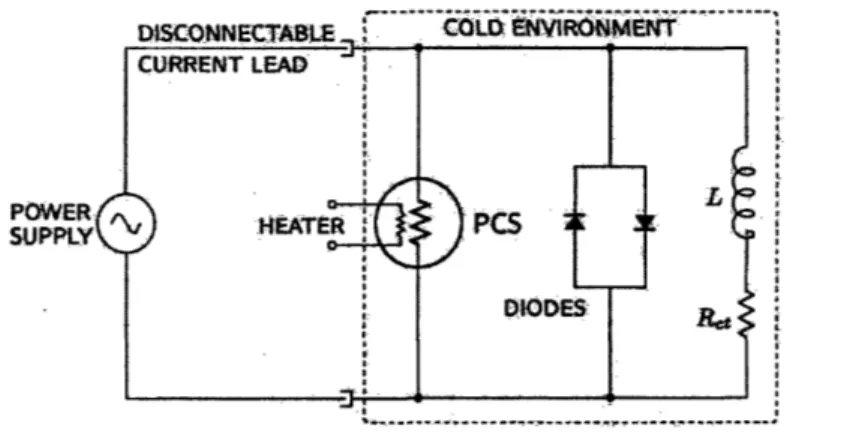
The MRI magnet circuit is shown below in Figure 1. The magnet portion of the circuit is entirely submerged in a cold environment (indicated by the dashed lines in the figure), usually maintained by liquid helium. The persistent-current switch (PCS) determines which loop the current travels through. To charge the magnet, the PCS is heated in order to remove the superconductivity and 'open' the switch. The power supply increases the current until the desired valued is reached. At this point the heater is shut off, allowing the electrical switch to cool back down to superconducting temperatures, thus closing the superconducting right side of the circuit. While effective, with this setup it is only possible to charge or discharge the magnet over a relatively long period of time (hours).
CO---ETAB----E OL---IRO
---USCONNECTABi~E COLOlb eEI~~liMU
Figure 1: This figure shows the basic circuit of a persistent-mode
superconducting magnet. The PCS switch determines which of the two paths the current will travel along [1].
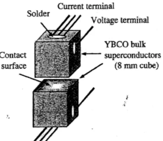
Replacing the PCS switch with a mechanical switch may enable the magnet to be charged or discharged in a short period of time. This switch would be made of an HTS compound, specifically, yttrium barium copper oxide (YBa2Cu307), also known as YBCO, which has a high critical temperature of 92
i I i 1 1 i I i i i 1 r r i i i I i I r i I I
K [2]. As shown in Figure 2, these two disks can be physically moved into and out of contact. The insulated area surrounding the switch could then remain at 4.2K, eliminating the need for the heater entirely, and thus eliminating all problems caused by the heater. While the disks are pressed together, the current will only run in this second loop and produce the high magnetic field desired.
Current terminal Contact surface Voltage terminal YBCO bulk superconductors S(8 mm cube) /i~
Figure 2: This figure shows a schematic view of a possible design for
the mechanical switch. Current leads are soldered to two separate pieces of YBCO which can then be moved into and out of contact. [3]
When the disks are apart, the switch would produce an infinite resistance and prevent the current from continuing through this superconducting loop, forcing it
to continue through a non-superconducting shunt resistor (not shown in Fig. 1).
Once the system is ready, the switch would easily be closed (by pressing the two disks together) and the magnet loop will become superconducting again,
provided that the magnet itself can be kept superconducting during a rapid charging or discharging process. This is another important issue, but outside the focus of this thesis work.
A malleable metal is ideal for the connection between the two YBCO disks. When the disks are pressed together, a soft material can conform and fill
in any slight imperfection on either surface, making a solid contact. Since most solders are malleable materials, a superconducting solder would be ideal for use in this mechanical switch.
Theoretical Analysis
Static resistivity is a material property that is measured in ohm meters
(Rm) and defined by R-A
p-
(1)
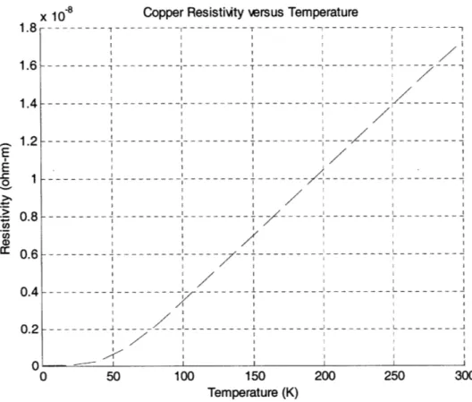
where R is the measured electrical resistance in ohms (0), A is the cross-sectional area of the sample in meters (m2), 1 and is the length of the sample (m) through which the current runs. Resistivity varies as temperature changes, decreasing as temperature also decreases. This relationship generally looks linear at first, until the element reaches the lower temperatures. Figure 1 below shows the
x 10-8 Copper Resistivity versus Temperature
1.8--- --- --- -I I I I -1.6 - - - - , 1.4 - --- r--- ,--- I I I 0.4 ---0 .2 -- ---- --- - ---- -- --- - -- ------ --- L ---- J 0 50 100 150 200 250 300 Temperature (K)
Figure 3: This graph shows the resistivity of copper as a function of its
temperature. The lowest value the resistivity reaches is 20
resistivity of copper as a function of temperature. The relationship seems to lose
its linearity at temperatures below 75K.
For many elements, there is a transition temperature (critical temperature) where the material becomes super-conducting; that is, its resistivity drops off to
zero, becoming negligible no matter the current. As shown in Figure 3 above, copper never reaches superconductivity. The magnitude of the resistivity never drops off to zero. Table 1 shows the transition temperatures of three elements
that can become superconducting: indium, lead, and tin. Some solder alloys are
made from varying concentrations of these elements. Four such solders are
tested in this experiment.
Table 1: This table shows the known superconducting critical temperature of three elements from two different sources. These elements make up the solder alloys that were tested.
Element Source 1 [5] Source 2 [6]
Indium (In) 3.37 3.41
Lead (Pb) 7.22 7.20
Tin (Sn) 3.73 3.72
Table 2 shows the solder alloys tested in this experiment. Given that the
critical temperature of lead is over twice that of either tin or indium, alloys with a higher lead concentration have a higher transition temperature. Only two of the solders currently have a known transition temperature.
Table 2: Solders tested along with the known transition temperatures. [7]
Alloy Temperature [K]
501n/50Pb 6.35
601n/40Pb
-50Sn/50Pb 7.75
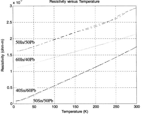
Hiroyuki Fujishiro, a research scientist and professor at Iwate University in Iwate, Japan, has conducted cooling experiments with these four solders. For the first two alloys, the resistivity data (as a function of time) was collected from 10K
until room temperature, or approximately 300K. There is no indication that the 50/50 or 60/40 indium/lead compound achieves superconductivity before 10K. A
second experiment included the resistivity data for the two tin/lead solders from 6K to 300K. Figure 4 displays each data set simultaneously as a function of temperature. The indium-lead alloys had higher resistivity values overall, with the 50/50's resistivity about one and half times the 60/40. The tin-lead alloys, however, nearly shared an identical curve with each other, only slightly
x 10" Resistivity versus Temperature
2.5
0.5
0 50 100 150 200 250
Temperature (K)
Figure 4: This figure shows the data collected in two set of experiments by Fujishiro. The indium-lead experiments were not tested below 10K and therefore show no transition to superconductivity. [8]
I -yJ - - - -- ----- IL - - -- -- - -II I S -- - I 50In/5OPb 60In/40Pb -- I - - - -40Sn/60Pb S S 50Sn/50Pb 300 Jp*/ ~I-r~ _l_________i______ r- -- -
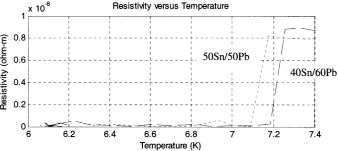
-separating below 200K. At about 7K, there is a clear drop off in the resistivity values. Figure 5 zooms in on this transition into superconductivity. Even though the resistivity prior to the transition is on the order of nanos, there is a clear and distinct drop to zero.
x 10-8 Resistivity versus Temperature
E1
E 0.8
o 0.6 > 0.4 c0.2 60Pb 6 6.2 6.4 6.6 6.8 7 7.2 7.4 Temperature (K)Figure 5: A zoom in of the lower left corner of Figure 4. Both alloys clearly reach superconductivity between 7.1 K and 7.3K.
There are other elements, such as bismuth strontium calcium copper oxide (known as BSCCO-2223 or Bi-2223), that have the ability to reach superconductivity at a much higher temperature than naturally occurring elements. BSCCO-2223, a man-made compound with a chemical equation of (BiPb)2Sr2Ca2C3010o, reaches super conductivity at approximately 110K [9]. This
characteristic makes it very useful in superconducting systems requiring less cooling capability.
Apparatus and Setup
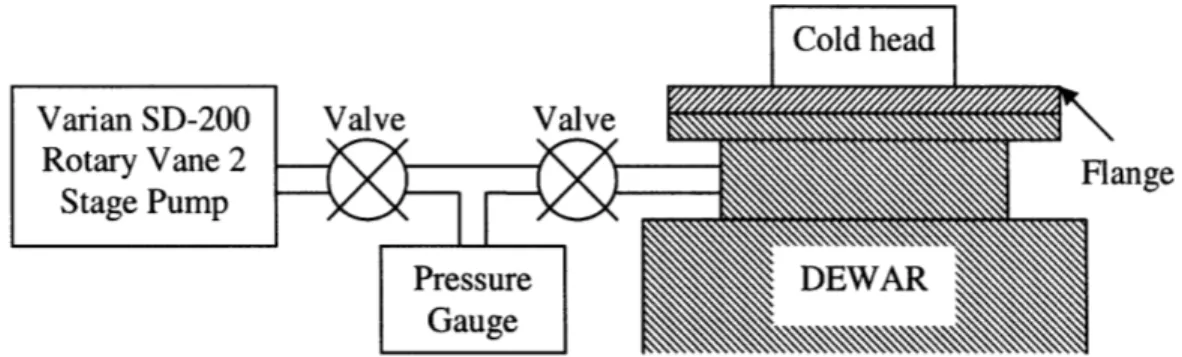
A bucket-type Dewar (cryostat) was used to create an insulated environment that can be lowered to such temperatures. The cryostat seal consisted of a tight-fitted flange reinforced by a rubber o-ring coated in Dow Corning@ High-Vacuum Grease. A Varian SD-200 Rotary Vane 2 Stage Pump was used to evacuate the chamber to less than 1 millitorr to reduce sample heating by convection. Figure 6 shows the schematic of the pump's connection to the Dewar.
Figure 6: A basic schematic for the outside of the system. The vacuum
pump is used to empty the vacuum sealed chamber when the system is closed and data is collected.
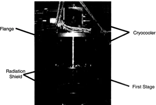
Cooling is provided by a Sumitomo RDK-408 cryocooler bolted to the center of the cryostat flange, as shown in Figure 7. This cryocooler has two stages with cooling capacities of 37 Watts at 40K and 1 Watt at 4.2K at the first and second stage respectively. A copper radiation shield approximately 60 centimeters tall and 20 centimeters in diameter (shown open in Figure 7) hangs from the first stage of the cold head. It entirely encompassed the second stage of the cold head and the sample to help block radiation and conduction heat transfer.
Flange
Radiation Shield
Cryocooler
First Stage
Figure 7: Top flange shown outside of the Dewar. The lid of the radiation shield is bolted onto the first stage of the cold head. The figure also shows the cryocooler mounted on the top flange.
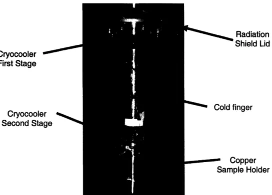
The rest of the cold finger is shown in its entirety sans radiation shield in Figure 8. A copper sample holder is securely bolted to the second cooling stage of the cold finger. Apiezon-N Grease was applied to the two contacting surfaces to ensure a strong thermal conductivity.
Cryocooler First Stage Cryocooler Second Stage Radiation Shield Lid SCold finger -* Copper Sample Holder
Figure 8: This figure shows the part of the cold finger and sample that is protected by the radiation shield. The sample holder is bolted tightly to the second stage of the cryocooler.
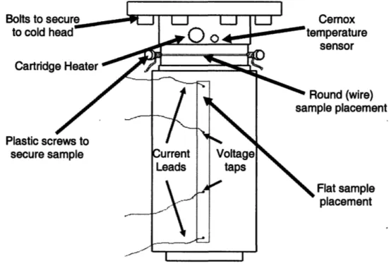
The copper sample holder schematic view is shown in Figure 9. The outer
layer of the copper sample holder was coated in GE Thermosetting Adhesive and
Insulating Varnish in order to electrically insulate while allowing excellent thermal
conductivity. Two holes were drilled in the copper holder. The larger tightly fit a 50W/500 cartridge heater. The smaller securely held the temperature sensor, a calibrated Lake Shore canister Cernox (model CX-1050-AA-4L, serial X43264) with a temperature range of 4.00K to 325K. Both the heater and the Cernox were coated in a white EG&G Type 120 thermal joint compound before being inserted into the sample holder. Samples were tested either in the form of a round wire and/or in the form of a flat tape. Wires were pressed along the arc of the copper and secured by wrapping each end around a plastic screw. Kapton tape was
used to ensure the wire along the arc was in full contact with the copper. Current was provided via AWG 33 copper wire and alligator clipped to the ends of the solder. Two voltage taps of AWG31 copper wire were then hooked on at a set distance from each other (at first at approximately 16 centimeters apart, later at 4 centimeters apart). The flat strips of solder sample were placed vertically on the shaft of the copper, electrically insulated by Kapton tape and secured by the GE varnish. Cerrolow-117 alloy, a low temperature solder, was used to attach four copper leads (AWG 34) to the solder sample without damaging it. Two leads were placed at each end of the flat sample to connect to the current leads. The other two leads were centered on the sample, placed approximately 3 centimeters apart. Cernox ,mperature sensor lound (wire) 1ple placement Flat sample placement
Figure 9: This figure shows all facets of the copper sample holder. Carefully sized holes were made for the heater and temperature sensor.
Wire samples were securely placed around the smaller diameter of the mass and wrapped around the two end plastic screws. Flat samples were secured by varnish and attached right to the shaft.
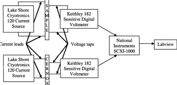
The circuit of the sample had two variations. When continuous data was
collected as a function of time via LabView, the sample and the Cernox had similar circuits, as shown in Figure 10. Two Lake Shore Cryotronics 120 Current Sources independently provided different steady current to the sample and the Cernox. The voltage across both the sample and the Cernox was then collected by two separate Keithley 182 Sensitive Digital Voltmeters. The voltmeters acted as amplifiers and provided a gain that varied inversely proportionally to the range setting on the device. Both voltmeters output their amplified voltages into different channels of the National Instruments SCXI-1000 Module, which were then recorded into text files by the LabView program on the computer. Matlab scripts were used to import the Cernox and sample data files and convert the voltages to temperature and resistivity, respectively.
Figure 10: The flow diagram shows the circuits for both the sample and the temperature Cernox for when data is collected continuously as the sample is either cooled or allowed to warm up. The current is provided by two separate, constant current sources, with two voltmeters simultaneously collecting the data, amplifying it, and outputting it.
When individual data points were collected at specific temperatures and manually recorded into Excel, the cartridge heater was used and regulated by a Cryo-Con 32B Temperature Controller. The circuit for the sample no longer uses the circuit back to the computer and LabView; instead values are read directly from the voltmeter and recorded in an Excel spreadsheet. Figure 11 below shows this alternate circuit for the temperature Cernox. The temperature controller provides the current and collects the voltage for the temperature data, converting it to temperature in Kelvin. The controller adjusts the wattage of the heater in order to produce and maintain the desired temperature.
taps
Figure 11: This flow diagram shows the alternate circuit for the Cernox.
It allows the collection of data at a specifically set temperature. The temperature control both provides current and measures the voltage, all the while adjusting the heater in order to establish a constant temperature.
When using the Lake Shore current source for the temperature data collection, the current to the Cernox was set constant at 3 microamps. The range on the voltmeter was set to 30 microvolts in order to produce a gain of 100. The current source and voltage range (and therefore the gain) required for the sample circuit, however, varied depending on the material being tested.
Experimental Procedure
For each set of continuous warm-up data, the first Cernox configuration was used, as shown in Figure 10. The sample was first cooled at maximum power to below 4K. As the sample cooled, the main chamber of the cryostat was evacuated. Within two hours, the temperature and pressure of the chamber became less than 4K and 1 millitorr, respectively. Once the temperature was at this steady state for at least an hour, the valve to the main chamber was closed to seal the vacuum. The combined offset of the voltmeter and the module for both the Cernox and the sample circuit were then recorded into LabView for a few minutes and collected into one text file, while the current sources were off. The current sources were then turned on at a set value, and both the temperature and sample data was simultaneously recorded into a second LabView. After LabView had logged a few minutes of data points at this minimum temperature, the cryocooler was turned off and the system was allowed to warm up while LabView collected data points at a frequency of either once or twice a minute.
The alternate Cernox configuration, as shown in Figure 11, was used for individual data point collection at various set temperatures for some samples. For each test, the system was cooled in the same way as the continuous data collection. The Cryo-con temperature controller was then set to various temperatures and given some time to stabilize before recording data. Once the temperature was constant for five or ten minutes, data points were recorded into
In each test, the sample's dimensions were carefully measured and recorded, along with the precise distance between the voltage taps. For both data collections, these values, along with the current value, were included in the Matlab code or the Excel spreadsheets in order to convert the voltage across the sample to resistivity. The resistivity values from various tests for the same material could then easily be compiled and compared amongst themselves, no matter the current or the sample dimensions.
Results and Discussion
A copper test run as performed first to ensure the experimental setup could generate relevant. A long copper wire with a diameter of 1 millimeter was set up in the copper sample holder. Voltage taps placed 16 centimeters apart collected the data while a current of 500 milliamps ran through the wire. After the system cooled overnight, the copper data was continuously recorded as the sample warmed up to room temperature. Figure 12 below shows the dashed
x 108 Copper Resistivity versus Temperature
I.0 1.6 1.4 1.2 E 0: 1 > 0.8 CO S0.6 0.4 0.2 A 0 50 100 150 200 250 300 Temperature (K)
Figure 12: Data was collected for a copper sample and compared to the
theoretical data to ensure that the overall configuration of the setup was valid. The wire was 1 mm in diameter with voltage taps 16cm apart.
theoretical data plotted with the experimental data. The experimental data is on the correct order of magnitude, and correlates with the theoretical data. When the sample was at the lower temperatures, however, the experimental resistivity
I I :I I II I I T -I I I I I I I I I - - - -- - - - -Experimental - - -- -Theoretical I- -I I I - L
-never quite makes it as low as the theory. The high level of current could be heating the sample at the lower temperatures; to test this theory, future tests will be run with a lower current.
The first six test runs of the 501n/50Pb test run use a long a sample with voltage taps 16.5 centimeters apart. Each test had a different current flowing through the .762 millimeter diameter wire, starting with the same 500 milliamps as the copper data. After this first data run, continuous warm up data was collect with a current of 100, 50, 30, 10, and 3 milliamps. As the current decreased, the data sets became consistently closer to matching Fujishiro's original data. Figure 13 simultaneously plots the two current extremes along with Fujishiro's curve.
x 10-7 501n/5OPb Resistivity versus Temperature
2.8 2.6 =2.4 a 2.2 a: 2 1.8 1 0 50 100 150 200 250 300 Temperature (K)
Figure 13: The plots include the first and last data run for the .762mm diameter sample of 501n/5OPb with voltage taps 16.5cm apart. In the six data runs, the date consistently improved its correlation with Fujishiro's previously found curve as the current decreased.
Both data sets have similar slopes, but the 3 milliamp data is the closest to mirroring Fujishiro's previous data.
It is important to note, however, that although the critical temperature of the 501n/50Pb is 6.35K, none of these first six data runs showed the solder becoming superconductive, despite reaching temperatures below 4K. It is possible that one reason for this is the low voltage produced by the low current allows for too much noise. Thus, prior to the subsequent data sets, another parameter was changed; the distance between the voltage taps was reduced.
Figure 14 shows the next three sets of data collected at low currents (3 and 10 milliamps) from voltage taps 3.97 centimeters apart. The plots no
S10-7 501n/50Pb Resistivity versus Temperature
3mA I=m
---
~-----
-L
--
---II -- - - -- I---- I II I I
Fui ishiro
-- -- --- --- ~--- --- --- 11---1 11 I I I 0 50 100 150 200 250 300 Temperature (K)Figure 14: The low current plot for the first few data runs of a .762mm diameter sample of 501n/50Pb with voltage taps 3.97 cm apart. The data sets are erratic and don't even correlate when the same current is used.
3.0 3 E 2.5 --U, S2 1.5 1
longer correlate well with Fujishiro's data. The data is very erratic; the two sets taken using 3 milliamps don't remotely resemble each other, Fujishiro's curve, or the original data set collect with the voltage taps 16.5 centimeters apart. The data
sets collected using 30 and 100 milliamps, however, correlate very well with Fujishiro's data, as shown in Figure 15 below. The data lines collected are nearly indistinguishable from each other, despite their different current settings.
x 10-7 501n/50Pb Resistivity versus Temperature 3 2.5 E S2 EIc 0 50 100 150 200 250 300 Temperature (K)
Figure 15: The same .762 mm diameter sample of 501n/50Pb with
voltage taps 3.97 cm apart is plotted here, but with two higher currents, 30 and 100 mA. The curves correlate excellently with each other and with Fujishiro's curve.
It is important to note again, that the data does not show a transition to superconductivity. Fujishiro I I I -- - - - ---I I I II I 30mA
The next sample tested, 601n/40Pb, had a diameter of .762 millimeters as well, with the voltage taps placed 4 centimeters apart. All data runs were
performed using 100 milliamps of current. As Figure 16 shows below, the
multiple data sets are nearly indistinguishable. The sets are also parallel to Fujishiro's data, but the values are unfortunately off by about 25%. Once again, no transition is observed.
x 10-7 601n/40Pb Resistivity versus Temperature
2.6
2.4 2.2
0 50 100 150 200 250
Temperature (K)
Figure 16: This sample of 601n/40Pb has a .762 mm diameter with voltage taps 4 cm apart. Both curves represent data taken using 100
mA. They correlate excellently with each other, but are off by about 25%. The 40Sn/60Pb sample of solder wire had a diameter millimeters and voltage taps once again separated by 4 centimeters. sample of this solder was also heat treated and flattened to see if could produce better results. The tape was 71.83 millimeters
of 1.5748 A second a flat strip long, 4.15 I I I I II II III II I I I, --- r---I-~ -- -.- - -I -' - ---I I .1 I SI i II ImI I .. .. .... I"::I: I I I . ' IBI ... . >---- 0m --- I o" ' :--- ---- ---- I- rI - ---- -I .o '"I I AL: I.. Ii ...."I Il ~---1---- 4.--- -- -... II I... I '°' II I I I I I II I 300
millimeters wide, and .34 millimeters thick. The voltage taps were centered on the strip, 31.61 millimeters from each other. Both samples were supplied with 100 milliamps of current. Figure 17 below shows that the flat data was numerically off by a larger factor than the data collected with the wire sample. The dashed line in the middle represents Fujishiro's data, and the small 'x's in the corner are once again the manually collected temperature controlled. The wire solder continuously collected data does correlate with the temperature controlled data of the same sample. None of these setups or methods, however, was able to record the alloy become superconducting.
x 10-7 40Sn/60Pb Resistivity wersus Temperature
II I FlatSapl I
---
t---
---r---
-
•--
---F :" I. I ,;•. " • I _ -- -- -- -- - --- ---Round Sample --- --- -- - - ---" -" ' "II -. ., I "I I II I II I I __I . '' I I I 0 50 100 150 200 250 300 Temperature (K)
Figure 17: The 40Sn/60Pb alloy was tested (using 100mA) as a around
wire and flat tape. The round wire continued to produce the data closest to Fujishiro's. 1.8 1.6 1.4 E 1.2 > 1 S0.8 0.6 0.4 0.2 A
The 50Sn/50Pb alloy was also tested in both configurations. These curves, however, more closely correlated than the previous alloy. The dashed line in Figure 18 represents Fujishiro's data, while the continuous data set is that of the flat tape (30.88 millimeters long, 3.61 millimeters wide, and 0.34 millimeters thick). The asterisks data was manually collected from the round wire sample, using the temperature controller. However, once again, neither configuration nor recording method shows the alloy becoming superconducting.
x 10.7 50Sn/50Pb Resistivity versus Temperature
1.8 --- - - - - - -T --- - - - ---I I I I / I I I I 1.6 --- T --- --- --1.4 ---- --- --- ---I I I II I I I 1.4 -
---0 .8
---
I1
---
I - I I I Il 0I 6-E 1--- I I I Ir I S0.8A--- ---- - --- 0.4 0.2 II I i .j - III --- 1---_- I ---I l II III I I I I I I t I I I I ,, ,, ,, U, 0 50 100 150 200 250 300 Temperature (K)Figure 18: The two samples of 50Sn/50Pb alloy were shaped differently, but supplied with the same 100 mA of current. The data was collected through the two different methods as well. The values are on the same order of magnitude, but start to differ by a greater factor at the warmer temperatures.
Since no critical temperatures were observed, both the continuous and the temperature controlled experiments were performed on a 7 centimeter piece of
BSCCO tape, the high temperature superconducting tape. The two voltage taps were centered at 30.2 mm apart and a 100 milliamp current was supplied. Figure 19 below shows both data sets plotted together, the red 'x's marking the individual points manually collected. The BSCCO clearly becomes superconducting around 112-113K, comparable to the literature value of 110K.
x 10-9 BSCCO Resistivity versus Temperature
100 150
Temperature (K)
200 250 300
Figure 19: This plot shows both the continuous warm up of the BSCCO tape as well as the individual points manually taken with the temperature controller. The tape clearly becomes superconducting at around
112~113K
I I I
I I
Conclusion
With the exception of the BSCCO tape, none of the data collected showed the alloys becoming superconducting. Relatively higher currents (100 mA) and small samples, however, did produce more consistent data that often did correlate with other data within this experiment, or in Fujishiro's.
There are a few possible reasons why the alloys were never recorded becoming superconducting. It is possible that the devices and tools used in the experimental setup were not sensitive enough to measure the superconducting phenomenon at the low voltages experienced at such low temperatures. The equipment may have been improperly calibrated. The wiring between the sample and devices also could have added extra noise that resulted in an immeasurable
offset which the overshadowed any changes in the small voltage.
It is also possible that the temperature read by the Cernox was not the actual temperature of the sample. The Cernox actually technically measures the temperature of the copper sample holder. The sample may not have had an excellent thermal contact and therefore the sample itself never actually reached the low temperatures the Cernox was reading. The current running through the sample also may have caused some heating that prevented the samples from reaching those critical temperatures. The Cernox would also have failed to feel such a heating due to its placement.
In order to improve this experiment, more sensitive equipment would be needed. All offsets would need to be minimized as much as possible. The temperature sensor would also need to have a more direct thermal contact with
the sample itself, to ensure that the temperature being recorded is actually the temperature of the sample. Establishing a better contact with the cold finger, or whatever the cooling system may be, would also help to improve the results.
Sources
[1] Yukikazu Iwasa, Case Studies in Superconducting Magnets: Design and
Operational Issues 2nd Ed. (Plenum Press, New York, not yet published). [2] Thomas P. Sheahen, Introduction to High-Temperature Superconductivity.
(New York: Putnam Press, 1994).
[3] K. Sawa, M. Suzuki, M. Tomita, and M. Murakami, "A fundamental behavior
on mechanical contacts of YBCO bulks," Physica C: Superconductivity 378,
803 (2002).
[4] David R. Lide, CRC Handbook of Chemistry and Physics 75th Ed. (CRC Press, Boca Raton, 1994:12-41).
[5] F. Din and A.H. Cockett, Low Temperature Techniques. (Interscience
Publishers, Inc., New York, 1960).
[6] P.V.E. McClintock, D.J. Meredith, and J.K. Wigmore, Matter at Low
Temperatures. (Blackie & Son Ltd, London, 1986).
[7] W.H. Warren and W. G. Bader. "Superconductivity measurements in solders
commonly used for low temperature research," Review of Scientific
Instruments 40 (1969).
[8] Hiroyuki Fujishiro. (Iwate University, Japan, unpublished data, 2006-2007). [9] Jack W. Ekin, Experimental Techniques for Low-Temperature Measurements:
Cryostat Design, Material Properties, and Superconductor Critical-Current Testing. (Oxford University Press, New York, 2006).