HAL Id: hal-00022158
https://hal.archives-ouvertes.fr/hal-00022158
Submitted on 3 Apr 2006
HAL is a multi-disciplinary open access
archive for the deposit and dissemination of sci-entific research documents, whether they are pub-lished or not. The documents may come from teaching and research institutions in France or abroad, or from public or private research centers.
L’archive ouverte pluridisciplinaire HAL, est destinée au dépôt et à la diffusion de documents scientifiques de niveau recherche, publiés ou non, émanant des établissements d’enseignement et de recherche français ou étrangers, des laboratoires publics ou privés.
Comparison of various lithography strategies for the
65-and 45-nm half pitch using simulation
David Fuard, Patrick Schiavone
To cite this version:
David Fuard, Patrick Schiavone. Comparison of various lithography strategies for the 65- and 45-nm half pitch using simulation. 2004, pp.1360-1374. �hal-00022158�
Comparison of various lithography strategies
for the 65- and 45-nm half pitch using simulation.
D. Fuard, P. Schiavone,
Laboratoire des Technologies de la Microélectronique - CNRS,
c/o CEA Grenoble, 17 rue des Martyrs, 38054 GRENOBLE cedex 9, France
ABSTRACT
At present, the question of the move from 193 to 157nm lithography is under discussion. There are still several major issues such as the development of 157nm photo-resists and pellicles, as well as calcium-fluoride lens material availability. The extension of the 193nm lithography down to the 65- and 45-nm half pitch technologies is now considered as a serious alternative. This requires several technical challenges with the use of phase shift masks (PSM), optical proximity effects corrections or liquid immersion.
Simulation gives information on expected process latitudes and is an important tool to help this technical choice. Previous works [1,2] have shown that the "Diffused Aerial Image Model" (DAIM) [3] is accurate for CD prediction. Reliable process latitudes can be extracted from the simulated focus-exposure matrices (FEM). The model is used for the process latitudes evaluation of the different lithography approaches possibly used to print the 65- and 45-nm half pitches.
193nm illumination in addition to PSM is compared to 157nm lithography associated with conventional or optimized illumination schemes. This work shows that PSM at 193nm gives generally better exposure latitude for all pitches and CD, and confirms that 193nm lithography is a possible alternative to achieve 45nm and 70nm half pitches patterning. The process windows are nevertheless very small, and huge mask error factors (MEEF) are another sign that printing such small features is close to the physical limit (k1 factor close to the quarter).
Keywords: Lithography simulation, 157nm lithography, immersion lithography, PSM, DAIM, aerial image, CD prediction, OPC.
1. INTRODUCTION
The use of simulation for CD prediction is often mandatory to avoid heavy experimental work and to decrease the cost of R&D. Recent works enlight that simplified resist models offer similar CD prediction reliability compared to full resist models, despite the fact that the latter are based on fundamental physical considerations. In addition, full resist models are very difficult to tune and the large number of required parameters is a major source of simulation to experiment mismatch [4].
We have shown [1] that the Diffused Aerial Image Model (DAIM, which consists only in a convolution between the aerial image and a given mechanical noise) exhibits the best CD prediction reliability/simplicity ratio. This model is also the one that used the less correlated parameters [5]. In this paper, the comparison results of lithography strategies for the 65- and 45-nm half pitch are based on the use of the DAIM. The work first consist in extracting model parameter by a fitting procedure, for both 193nm and 157nm resists. Then these parameters are used with several illumination conditions and masks for FEM computation, from which process latitudes (Exposure Latitudes for given defocus latitudes, MEEF, ...) are calculated.
We present the results of Exposure Latitude for PSM @ 193nm and for 157nm using various lithographic approaches. These results are correlated with the determination of the optimum Numerical Aperture / Partial Coherence couple for a given mask design (CD lines and pitch). This helps to evaluate which lithography strategy is the most promising between PSM at 193nm and BIM at 157nm for the 65- and 45-nm half pitch. In reality, it is well known that the option used for a lithography process is extremely dependent of each company and of the manufactured product. The goal here is rather to draw trends and give first order conclusions (whenever it is possible, i.e. when compromises and/or fine optimization is not involved in the choice).
In a first step, we have performed a comparison of 65- and 45-nm CD process latitude between 193nm + alternating PSM (conventional illumination) and 157nm + binary mask (conventional and annular illumination). This work is completed by the determinations of optimum couple Numerical Aperture NA / partial coherence σ (as a function of the pitch) and Mask Error Factor (MEEF) for the previous lithography conditions. A additional comparison of exposure latitude between various lithography strategies at 157nm complete the expected exploration of the 157nm strategy. The impact of the 157nm resist "maturity" on DAIM parameters extraction and process latitudes is also discussed.
2. EXPERIMENTAL
2.1 Datasets
The 193 and 157nm experimental data used to calibrate the resist model are respectively obtained with an ASML /900 stepper (using a Sumitomo PAR 707 resist) and a 157nm micro stepper (using a Shipley XP1664 prototype resist). The available datasets for 193- and 157-nm resist parameters extractions are listed below, and the detailed experimental conditions are summarized in Table 1.
Lines at 193nm:
The features were obtained with 0.5µm thick Sumitomo PAR 707 resist on 75nm thick anti reflective coating AR19. For the exposure, we used an ASML/900 193nm stepper with conventional illumination and Binary Masks (BIM). The nominal CD of the lines on the mask are 120nm with a set of nested and isolated lines (line to space ratios L:S = 1:1.5, 1:1.75, 1:2, 1:3 and isolated), using 0.63 NA and two different partial coherences of 0.6 and 0.85. This provides a set of ten different settings on which the simulation parameters are adjusted. A Hitachi Critical Dimension Scanning Electron Microscope (Hitachi S9300 SEMCD) is used for CD measurements.
Lines at 157nm:
The final features were obtained using 0.11µm thick Shipley XP1664 resist (on 117nm AR19 anti-reflective coating), conventional illumination and alternating Phase Shift Mask (alt-PSM), with a Exitech micro exposure tool (numerical aperture (NA) of 0.6, and partial coherence (σ) of 0.3). The nominal CD of the lines on the mask are 60, 70 and 90nm, with respectively different Space to Line ratios L:S = 1:1, 1:5, and 1:10. The final features widths are measured via SEM cross-section.
2.2 Background: Model description and calibration
The DAIM has been used as a base line for this work.[1] The principle of the DAIM is to compute the CD from the aerial image only.[3] It is based on the hypothesis that the resist has a threshold-like behavior. The intensity distribution used for the CD extraction is obtained by a convolution of the standard aerial image with a gaussian which width is an adjustable parameter of the model. CD and dose offsets are added that improve the accuracy of the simulations, and finally the DAIM uses only four parameters. A previous work [2] show that the DAIM is predictive and can simulate accurately CDs outside the set of data that have been used for fitting the model parameters.
The DAIM coefficients depend of the whole resist process (resist thickness, layer stack, PAB, PEB, development conditions), and metrology conditions. They are of general use and they should be the same for all feature types, pitches, and optical settings. The model parameters are calibrated with FEM experimental data. The resist parameters extraction is performed using a global fitting procedure. This fit is based on functions that rely on physical considerations and that include the isofocal dose or threshold as explicit coefficients.[2] The four DAIM parameters are drawn together.
All the masks and optical tools considered for the following work are considered as perfect (for process windows evaluation, it is highly improbable that non ideal objects would lead to improved process margins). No mask correction has been applied in the simulations.
Using this method, the simulation accuracy for the Sumitomo PAR707 resist is around 4%. This accuracy reaches 10% for Shipley XP1664 157nm resist, mainly because of rather noisy available experimental data. The DAIM parameters extraction results for these both resist processes are gathered in Table 2.
3. RESULTS & DISCUSSIONS
3.1 Optimum Numerical Aperture (NA) and partial coherence (σσσσ) evaluation
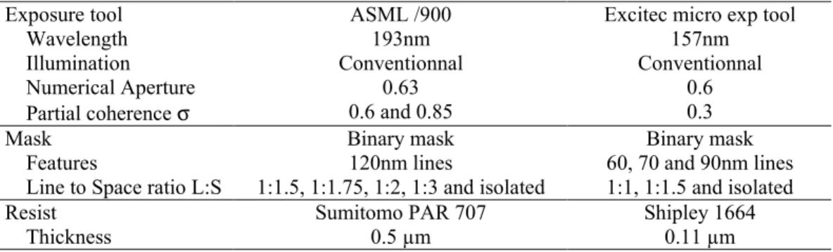
The illumination conditions as well as the numerical aperture of the lens have been used as parameters in order to target at optimized optical settings for each feature type. The exposure latitude (@0.2µm DOF) is plotted on Figure 1, Figure 2 and Figure 3 (respectively 157nm+BIM+conventionnal illumination, 157nm+BIM+OAI and 193nm+PSM). Each graph corresponds to a contour plot in the NA-σ space for a specific space to line ratio ranging from 1:1 to isolated (1:100). NA has been varied from 0.5 to 0.9 (step 0.05) and partial coherence σ from 0.1 to 0.5 for PSM and from 0.4 to 0.9 for BIM.
Figure 4 and Figure 5 show the optimum NA and partial coherence respectively that provides the best exposure latitude (@0.4µm DOF) for each space to line ratio. At first, we can see as expected that smaller pitches (for the same line CD here) needs larger NA to be resolved. Looser features are better printed using smaller NA. Subsequently, Figure 5 shows that optimal partial coherence is close to be constant. Considering the pitch limit resolution Plim=λ/[NA(1+σ)]
formula, simulation results confirm that NA has the biggest impact on limit resolution for a given wavelength (because of 1+σ (with σ<1) impacts less Plim compared to NA).
3.2 Dose latitude comparison between PSM @ 193nm and BIM @ 157nm
First, we can see on Figure 1, Figure 2 and Figure 3 that the 1:1 pitch (130nm) is either hardly resolved or not printed at all, in all cases. Indeed, it is not surprising if we consider the physical limits of each lithographic process: the coherent cutoff for λ=157nm and NA=0.85 is 184nm. For 193nm + alt-PSM, with this NA, the coherent cutoff is 113nm. As expected, the Figure 1 and Figure 2 also show that 157+BIM (Conventional Illumination and OAI) exhibits better process latitude for semi-dense lines (L:S=1:2 or 1:3). For OAI, these simulation results confirm that OAI is usually optimized for a given pitch, and provides reduced process latitude outside this target. For 193nm + alt-PSM, Figure 3 confirms that more isolated features better process windows.
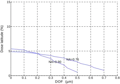
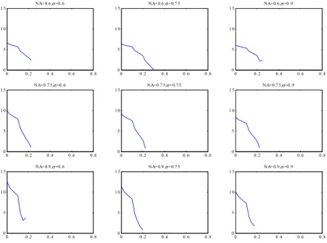
Another point is that 193nm + Alt PSM (Figure 3) provides better process latitude (>10% at maximum) than 157nm, even assisted by off-axis illumination (annular, with about 5% EL at best NA-σ), mainly because of lower coherent cutoff for 193nm + alt-PSM. 157nm only shows better performance for the 1:1 pitch. On these plots, we can also see that increasing the numerical aperture is not a guarantee to get a better process latitude for the largest pitches. This is even more true when more depth of focus is targeted. If for 0µm DOF, the maximum NA gives the maximum energy latitude, as illustrated on the EL-DOF curves of Figure 6 and Figure 7, we can see that starting from 0.2µm, the best NA has already shifted towards lower values NA. This fact is more pronounced for more isolated features. The curves for the larger NA show a smaller depth of focus than for lower NA. These graphs are for 193nm + PSM, but the same holds for 157nm + Binary mask. Figure 6 and Figure 7 show another general fact that DOF is smaller for isolated feature than for dense ones. This can also be observed for binary masks (Figure 8 and Figure 9) and all feature sizes.
The latitudes shown in Figure 10 are those obtained for the optimum settings for each feature. For 157nm imaging, the exposure latitudes @ 0.4µm DOF are smaller than 4%, they increase to ~6% if the DOF request is reduced to 0.2µm. For 193nm + alt-PSM, the latitude for very dense pitch is also very small. These features are close to the coherent cut-off. It means that if a single exposure strategy is used, the common process window will probably be zero. This can be overcome in some way using OPC or multiple exposure strategies. But for larger space to line ratios, increased latitude can be obtained. This finally shows that one hoped advantage of using 157nm to avoid strong RET developments is certainly not fulfilled.
3.3 Proximity effects & Mask Error Factor (MEEF) comparisons
Proximity effects are illustrated Figure 11 and Figure 12. The dose to size nominal CD as well as the dose to size CD+10% and CD-10% are plotted for various feature sizes, pitches and NA and σ. In relation to the very small process latitude, the difference in dose to size is very large between isolated and dense features. For example, looking at 65nm lines for 157nm+BIM (Figure 11), the difference in dose to size reaches 30%. This shows that such lithographic option cannot be used for the patterning of a mix of nested and more isolated features, if we consider that the dose latitude is only a few percent. The situation for the 193nm + PSM is almost as bad as 157nm (Figure 12).
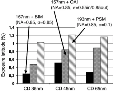
Mask enhancement error factor (MEEF) that represents the sensitivity to mask CD variations is another critical aspect of the low k1 lithography. For our target features, the numerical values are summarized in the bar graphs of Figure 13. Regarding the poor contrasts and process latitude, it is not very surprising to see very high MEEF values, reaching more than 25 at 157nm + BIM for both 45 and 65-nm CD nested lines. The values for PSM are much lower, between 15 and
20. For isolated lines, 193nm+PSM exhibits good MEEF value (close to 1), contrary to 157nm which reaches 5 and 2 respectively for 45- and 65-nm CD. Overall, these very high value are another aspect of the poor contrast imaging for printing of such small features at the low k1 targeted here. They have to be put in parallel with the poor process windows.
3.4 Simulation for 65nm half pitch: comparison between various approaches
The design rules to be simulated are related to the 2002 ITRS roadmap for the 65nm node. According to the type of circuit, the printed gate length is chosen to be 65nm for memory and 45nm and 35nm for other more demanding circuits. The half pitch is 130nm for every configuration. The exposure latitude @ 0.3µm depth of focus has been decided to be the target output number. The NA has been chosen at 0.85. This is not always the optimum value for these features. This means that improved results can be obtained for optimized optical settings, especially for PSM. We have also included isolated features in the simulation for comparison. Seven lithography candidates have been chosen: 157nm + BIM, 157nm + BIM + off-axis illumination, 157nm + 6% attenuated PSM, 157nm + alt-PSM, and 193nm + alt-PSM.
The dose latitudes @0.3µm DOF are presented in the bar graph of Figure 14. Except for the 157nm alt PSM and to a much lesser extend 193nm + alt-PSM, the latitudes are below 1%. This is again due to the very small pitch requested at this technology node. A relaxed pitch could probably gives more workable process margins for manufacturing. It is also again seen that 193nm + alt-PSM gives better results than 157nm. The aerial images at best focus for 193nm+alPSM and 157nm + BIM are shown in Figure 15. The contrasts summarized in Table 3 are very small for 157nm lithography (~3%). This also explains the minute process latitude. The same aerial images for isolated lines shows better contrast (Figure 16) which is consistent with the latitudes and the EL-DOF curves (Figure 17 and Figure 18). In the main, 157nm without strong RET seems to not offer improved process latitudes compared to 193nm+PSM for 65nm half pitch.
3.5 Sensitivity of 157nm simulation to DAIM resist parameters
The 157nm results used in the following are based on the resist currently available. Since the 157nm resist are still in a preliminary development phase, their performance is still far from being comparable to more mature 193nm resists. Improved resist materials and process can change the numbers especially as far as latitude is concerned. We have tried to infer what is the impact of the resist "maturity" by running 157nm simulation using model parameters derived from 193nm resists. Only the σ(noise) DAIM parameter has been kept the same (favorable to a better latitude because smaller σ(noise) leads to more contrasted diffused aerial images.).
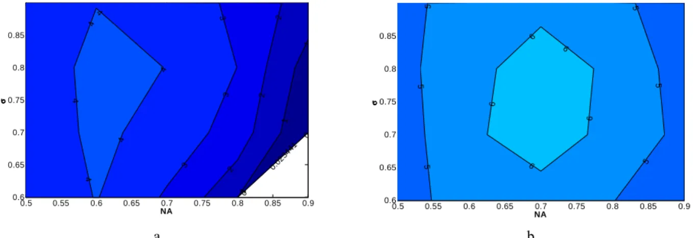
The results are illustrated in Figure 19. We can see on Figure 19b that the exposure latitude computed with the "193nm parameters" are slightly larger than the one computed using the regular model parameters. The difference is not negligible (~15%). However, it is not sure whether this can be attributed to a "maturity "effect". Indeed, parameters change can affect the position of the isofocal CD with respect to the target CD. This change can have important effect on the process latitude, especially in the situation where contrast are low like it is the case considered here. Finally, this work shows that 157nm resist development could have a non-negligible impact on effective process windows, and that global improvement of 157nm lithography is a key point for its mass manufacturing use.
4. CONCLUSION
It is shown that process latitude becomes very tight for design rules equal or below 65nm. In almost every case, in the current status of the resist, 193nm + PSM provides better performance than 157nm. Maximum dose latitude of about 1% for 45nm nested lines and 2% for 65nm nested lines are found (with a focus latitude of 0.4µm) whatever the lithography approach considered. For more isolated lines (using the same conditions as previously), PSM at 193nm exhibits dose latitudes close to 10%, whereas the dose latitude of the others lithography approaches do not increase. Phase shift mask in addition to 193nm exposure leads to process margin that are in almost every case larger than binary masks exposed at 157nm, even with the help of off-axis illumination. These figures are most of the time far from the currently targeted process margins (~8% EL @0.4µm DOF overlapping process window). This indicates that these lithographic options need an improvement by using optical enhancements. In addition, we have seen one more time that the use of high NA lenses does not always help to get an acceptable process latitude and MEEF are very high.
More generally, the 157nm development is facing up to now several major issues (such as photo-resists, pellicles, as well as calcium-fluoride lens material). These problems must be solved to make 157nm available for mass manufacturing (at the same maturity level between 157 and 193nm lithography and using the same RET, 157nm provides 20% smaller features compared to 193nm). Moreover, the choice to shift to 157nm is also an economic equation tightly link to the technical one. In addition, 193nm offers immersion solution that is on the way to be the solution of choice.
ACKNOWLEDGMENTS
193- & 157-nm experimental focus-exposure matrix data respectively provided by ST Crolles and IMEC. We thank again Serdar Manakli, Yorick Trouiller (ST) and Mieke Goethals (IMEC) for their cooperation.
REFERENCES
1. D. Fuard, M. Besacier and P. Schiavone, “Assessment of different simplified resist models”, SPIE Vol. 4691 pp.1266-1277 (2002).
2. D. Fuard, M. Besacier and P. Schiavone, “Validity of the diffused aerial image model: an assessment based on multiple test cases”, SPIE Vol. 5040 pp.1536-1543 (2003).
3. C. P. Ausschnitt, “Rapid Optimization of the Lithographic Process Window”, SPIE Vol. 1088, pp. 115-123 (1989). 4. A. Erdmann, W. Henke, S. Robertson, E. Richter, B. Tollkühn, W. Hoppe, “Comparison of simulation approaches
for Chemically Amplified Resists”, Proc. SPIE Vol. 4404, pp. 99-110 (2001).
5. B. Tollkühn and D. Matiut, “Resist models and calibration methods – what leads to predictive results?”, 1st IISB Lithography Simulation Workshop, Hersbruck (Germany), September 19–21 (2003).
Exposure tool ASML /900 Excitec micro exp tool
Wavelength 193nm 157nm
Illumination Conventionnal Conventionnal
Numerical Aperture 0.63 0.6
Partial coherence σ 0.6 and 0.85 0.3
Mask Binary mask Binary mask
Features 120nm lines 60, 70 and 90nm lines
Line to Space ratio L:S 1:1.5, 1:1.75, 1:2, 1:3 and isolated 1:1, 1:1.5 and isolated
Resist Sumitomo PAR 707 Shipley 1664
Thickness 0.5 µm 0.11 µm
Table 1: Summary of the experimental datasets
193nm resist 157nm resist σ(noise) 51 nm 42 nm
∆CD 27 nm 22 nm
a 6.4 mJ/cm² 32 mJ/cm²
b -2.2 mJ/cm² -4.0 mJ/cm²
Table 2: Relative mean CD difference error between simulated and experimental data for 193nm lines (Sumitomo PAR 707 resist)
157nm + BIM 157nm + OAI 193nm + alt-PSM
35nm CD 3.3 % 3.6 % 13 %
45nm CD 3.2 % 4.6 % 13 %
65nm CD 4.4 % 6.2 % 13 %
0.4 0.6 0.8 0.4 0.5 0.6 0.7 0.8 0.9 S ig m a L:S = 1:1 0 0 .0 0 6 5 1 4 2 1 1 2 0.4 0.6 0.8 0.4 0.5 0.6 0.7 0.8 0.9 L:S = 1:1.5 0 0 .4 2 0 1 4 1 2 3 3 4 0.4 0.6 0.8 0.4 0.5 0.6 0.7 0.8 0.9 L:S = 1:1.75 0 0 0 .98 7 5 2 1 1 2 2 3 4 5 0.4 0.6 0.8 0.4 0.5 0.6 0.7 0.8 0.9 L:S = 1:2 0 0 0 .38 97 512 3 4 5 0.4 0.6 0.8 0.4 0.5 0.6 0.7 0.8 0.9 NA S ig m a L:S = 1:3 01 2 2 3 3 4 4 0.4 0.6 0.8 0.4 0.5 0.6 0.7 0.8 0.9 NA L:S = 1:5 2 3 3 4 0.4 0.6 0.8 0.4 0.5 0.6 0.7 0.8 0.9 NA L:S = 1:100 2 3 4
Figure 1: dose latitude as a function of numerical aperture and partial coherence, for 0.2µm Depth Of Focus, 65nm CD lines, using 157nm lithography with Binary Mask.
0.6 0.8 0.5 0.6 0.7 0.8 O ff -a x is R a d iu s L:S = 1:1 0 0 0 .97 1 3 4 1 1 2 0.6 0.8 0.5 0.6 0.7 0.8 L:S = 1:1.5 0 0 .5 4 8 7 5 1 2 3 4 5 0.6 0.8 0.5 0.6 0.7 0.8 L:S = 1:1.75 0 1 1 .59 1 9 2 3 4 5 5 0.6 0.8 0.5 0.6 0.7 0.8 L:S = 1:2 2 3 4 5 5 6 0.6 0.8 0.5 0.6 0.7 0.8 NA O ff -a x is R a d iu s L:S = 1:3 3 4 4 5 5 0.6 0.8 0.5 0.6 0.7 0.8 NA L:S = 1:5 0 0 1 1 1.020 1 1.0 20 1 2 2 2 3 3 3 4 4 0.6 0.8 0.5 0.6 0.7 0.8 NA L:S = 1:100 1 2 3 4 4
Figure 2: dose latitude as a function of numerical aperture and partial coherence, for 0.2µm Depth Of Focus, 65nm CD lines, using 157nm lithography with Off-Axis Illumination.
0.6 0.8 0.1 0.2 0.3 0.4 0.5 S ig m a L:S = 1:1 01 0.6 0.8 0.1 0.2 0.3 0.4 0.5 L:S = 1:1.5 012 2.1 0 11 3 4 4 5 0.6 0.8 0.1 0.2 0.3 0.4 0.5 L:S = 1:1.75 0 0 1 1 1.1 6 2 7 2 3 4 56 6 7 0.6 0.8 0.1 0.2 0.3 0.4 0.5 L:S = 1:2 2 3 4 5 6 7 7 8 0.6 0.8 0.1 0.2 0.3 0.4 0.5 NA S ig m a L:S = 1:3 7 8 9 10 11 0.6 0.8 0.1 0.2 0.3 0.4 0.5 NA L:S = 1:5 1 2 3 4 5 6 7 8 9 9 10 1 0 1 112 13 0.6 0.8 0.1 0.2 0.3 0.4 0.5 NA L:S = 1:100 01 2 4 5 6 7 7 8 8 9 9 10 10 11 12
Figure 3: dose latitude as a function of numerical aperture and partial coherence, for 0.2µm Depth Of Focus, 65nm CD lines, using 193nm lithography with alt-PSM.
1 2 3 4 5 0.4 0.5 0.6 0.7 0.8 0.9 N A S/L ratio 157 OAI 157 BIM 193 PSM
Figure 4: optimum Numerical Aperture as a function of pitch, for: 157nm lithography with Binary Mask, 157nm lithography using Off-Axis Illumination, and 193nm lithography with alt-PSM.
1 2 3 4 5 0 0.2 0.4 0.6 0.8 1 S/L ratio P a r ti a l c o h e r e n c e 157 OAI 193 PSM 157 BIM
Figure 5: optimum partial coherence as a function of pitch, for: 157nm lithography with Binary Mask, 157nm lithography using Off-Axis Illumination, and 193nm lithography with alt-PSM.
0 0.1 0.2 0.3 0.4 0.5 0.6 0.7 0.8 0 5 10 15 NA=0.75 NA=0.90 DOF (µm) D o s e l a ti tu d e ( % )
Figure 6: Exposure latitude as a function of DOF for 65nm lines, S/L ratio of 2, 0.35 partial coherence, using 193nm lithography with alt-PSM, 0.75 and 0.90 NA.
0 0.1 0.2 0.3 0.4 0.5 0.6 0.7 0.8 0 5 10 15 NA=0.60 NA=0.75 DOF (µm) D o s e l a ti tu d e ( % )
Figure 7: Exposure latitude as a function of DOF for 65nm isolated lines, 0.35 partial coherence, using 193nm lithography with alt-PSM, 0.60 and 0.75 NA
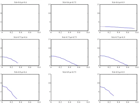
0 0 .2 0 .4 0 .6 0 .8 0 5 1 0 1 5 NA= 0. 6,σ=0 .6 0 0 .2 0 .4 0 .6 0 .8 0 5 1 0 1 5 NA= 0. 6,σ=0.7 5 0 0 .2 0 .4 0 .6 0 .8 0 5 1 0 1 5 NA= 0. 6,σ=0 .9 0 0 .2 0 .4 0 .6 0 .8 0 5 1 0 1 5 NA=0 .7 5,σ=0 .6 0 0 .2 0 .4 0 .6 0 .8 0 5 1 0 1 5 NA=0 .7 5,σ=0.7 5 0 0 .2 0 .4 0 .6 0 .8 0 5 1 0 1 5 NA=0 .7 5,σ=0 .9 0 0 .2 0 .4 0 .6 0 .8 0 5 1 0 1 5 NA= 0. 9,σ=0 .6 0 0 .2 0 .4 0 .6 0 .8 0 5 1 0 1 5 NA= 0. 9,σ=0.7 5 0 0 .2 0 .4 0 .6 0 .8 0 5 1 0 1 5 NA= 0. 9,σ=0 .9
Figure 8: Exposure latitude as a function of DOF for 65nm isolated lines, varying numerical aperture (row) and partial coherence (column), using 157nm lithography with Binary Mask.
0 0 .2 0 .4 0 .6 0 .8 0 5 1 0 1 5 NA= 0. 6,σ=0 .6 0 0 .2 0 .4 0 .6 0 .8 0 5 1 0 1 5 NA= 0. 6,σ=0.7 5 0 0 .2 0 .4 0 .6 0 .8 0 5 1 0 1 5 NA= 0. 6,σ=0 .9 0 0 .2 0 .4 0 .6 0 .8 0 5 1 0 1 5 NA=0 .7 5,σ=0 .6 0 0 .2 0 .4 0 .6 0 .8 0 5 1 0 1 5 NA=0 .7 5,σ=0.7 5 0 0 .2 0 .4 0 .6 0 .8 0 5 1 0 1 5 NA=0 .7 5,σ=0 .9 0 0 .2 0 .4 0 .6 0 .8 0 5 1 0 1 5 NA= 0. 9,σ=0 .6 0 0 .2 0 .4 0 .6 0 .8 0 5 1 0 1 5 NA= 0. 9,σ=0.7 5 0 0 .2 0 .4 0 .6 0 .8 0 5 1 0 1 5 NA= 0. 9,σ=0 .9
Figure 9: Exposure latitude as a function of DOF for 65nm 1:1 L:S nested lines, varying numerical aperture (row) and partial coherence (column), using 157nm lithography with Binary Mask.
1 2 3 4 5 0 2 4 6 8 10 12 14 D o se l a ti tu d e ( % ) S/L ratio 157 BIM 193 PSM 157 OAI
Figure 10: Exposure latitude as a function of pitch for 65nm lines, 0.4µm Depth Of Focus, using optimum numerical aperture and partial coherence.
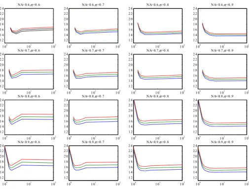
1 00 1 01 1 02 1 2 1 4 1 6 1 8 2 0 2 2 2 4 NA= 0. 6,σ=0 .6 1 00 1 01 1 02 1 2 1 4 1 6 1 8 2 0 2 2 2 4 NA= 0. 6,σ=0 .7 1 00 1 01 1 02 1 2 1 4 1 6 1 8 2 0 2 2 2 4 NA= 0. 6,σ=0 .8 1 00 1 01 1 02 1 2 1 4 1 6 1 8 2 0 2 2 2 4 NA= 0. 6,σ=0 .9 1 00 1 01 1 02 1 2 1 4 1 6 1 8 2 0 2 2 2 4 NA= 0. 7,σ=0 .6 1 00 1 01 1 02 1 2 1 4 1 6 1 8 2 0 2 2 2 4 NA= 0. 7,σ=0 .7 1 00 1 01 1 02 1 2 1 4 1 6 1 8 2 0 2 2 2 4 NA= 0. 7,σ=0 .8 1 00 1 01 1 02 1 2 1 4 1 6 1 8 2 0 2 2 2 4 NA= 0. 7,σ=0 .9 1 00 1 01 1 02 1 2 1 4 1 6 1 8 2 0 2 2 2 4 NA= 0. 8,σ=0 .6 1 00 1 01 1 02 1 2 1 4 1 6 1 8 2 0 2 2 2 4 NA= 0. 8,σ=0 .7 1 00 1 01 1 02 1 2 1 4 1 6 1 8 2 0 2 2 2 4 NA= 0. 8,σ=0 .8 1 00 1 01 1 02 1 2 1 4 1 6 1 8 2 0 2 2 2 4 NA= 0. 8,σ=0 .9 1 00 1 01 1 02 1 2 1 4 1 6 1 8 2 0 2 2 2 4 NA= 0. 9,σ=0 .6 1 00 1 01 1 02 1 2 1 4 1 6 1 8 2 0 2 2 2 4 NA= 0. 9,σ=0 .7 1 00 1 01 1 02 1 2 1 4 1 6 1 8 2 0 2 2 2 4 NA= 0. 9,σ=0 .8 1 00 1 01 1 02 1 2 1 4 1 6 1 8 2 0 2 2 2 4 NA= 0. 9,σ=0 .9
Figure 11: Proximity effects (dose to size CD ±10%) as a function of pitch for 65nm lines, varying numerical aperture (row) and partial coherence (column), using 157nm lithography with Binary Mask.
1 00 1 01 1 02 1 0 1 5 2 0 NA= 0. 6,σ=0 .2 1 00 1 01 1 02 1 0 1 5 2 0 NA= 0. 6,σ=0 .3 1 00 1 01 1 02 1 0 1 5 2 0 NA= 0. 6,σ=0 .4 1 00 1 01 1 02 1 0 1 5 2 0 NA= 0. 6,σ=0 .5 1 00 1 01 1 02 1 0 1 5 2 0 NA= 0. 7,σ=0 .2 1 00 1 01 1 02 1 0 1 5 2 0 NA= 0. 7,σ=0 .3 1 00 1 01 1 02 1 0 1 5 2 0 NA= 0. 7,σ=0 .4 1 00 1 01 1 02 1 0 1 5 2 0 NA= 0. 7,σ=0 .5 1 00 1 01 1 02 1 0 1 5 2 0 NA= 0. 8,σ=0 .2 1 00 1 01 1 02 1 0 1 5 2 0 NA= 0. 8,σ=0 .3 1 00 1 01 1 02 1 0 1 5 2 0 NA= 0. 8,σ=0 .4 1 00 1 01 1 02 1 0 1 5 2 0 NA= 0. 8,σ=0 .5 1 00 1 01 1 02 1 0 1 5 2 0 NA= 0. 9,σ=0 .2 1 00 1 01 1 02 1 0 1 5 2 0 NA= 0. 9,σ=0 .3 1 00 1 01 1 02 1 0 1 5 2 0 NA= 0. 9,σ=0 .4 1 00 1 01 1 02 1 0 1 5 2 0 NA= 0. 9,σ=0 .5
Figure 12: Proximity effects (dose to size CD ±10%) as a function of pitch for 65nm lines, varying numerical aperture (row) and partial coherence (column), using 157nm lithography with Binary Mask.
0 5 10 15 20 25 30 35 157nm + BIM
(NA=0.85, σ=0.85) 157nm + OAI(NA=0.85, σ=0.55in/0.85out) 193nm + PSM (NA=0.85, σ=0.1) CD 35nm CD 45nm CD 65nm M E E F 0 5 10 15 20 25 30 35 157nm + BIM
(NA=0.85, σ=0.85) 157nm + OAI(NA=0.85, σ=0.55in/0.85out) 193nm + PSM (NA=0.85, σ=0.1) CD 35nm CD 45nm CD 65nm M E E F 0 1 2 3 4 5 6 7 8 9 157nm + BIM (NA=0.85, σ=0.85) 157nm + OAI (NA=0.85, σ=0.55in/0.85out) 193nm + PSM (NA=0.85, σ=0.1) CD 35nm CD 45nm CD 65nm M E E F 0 1 2 3 4 5 6 7 8 9 157nm + BIM (NA=0.85, σ=0.85) 157nm + OAI (NA=0.85, σ=0.55in/0.85out) 193nm + PSM (NA=0.85, σ=0.1) CD 35nm CD 45nm CD 65nm M E E F a. b.
Figure 13: MEEF for the different lithography strategies (dose at targeted CD and defocus at best focus): a. 130nm pitch, b. isolated lines.
0 0,2 0,4 0,6 0,8 1 1,2 1,4 157nm + BIM (NA=0.85, σ=0.85) 157nm + OAI (NA=0.85, σ=0.55in/0.85out) 193nm + PSM (NA=0.85, σ=0.1) CD 35nm CD 45nm CD 65nm E x p o s u re la ti tu d e ( % ) 0 0,2 0,4 0,6 0,8 1 1,2 1,4 157nm + BIM (NA=0.85, σ=0.85) 157nm + OAI (NA=0.85, σ=0.55in/0.85out) 193nm + PSM (NA=0.85, σ=0.1) CD 35nm CD 45nm CD 65nm E x p o s u re la ti tu d e ( % )
0 0,1 0,2 0,3 0,4 0,5 0,6 0,7 -0,07 -0,02 0,03 N o rm a liz e d i n te n s it y defocus 157nm + BIM (NA=0.85, σ=0.85) 157nm + OAI (NA=0.85, σ=0.55in/0.85out) 193nm + PSM (NA=0.85, σ=0.1) 0 0,1 0,2 0,3 0,4 0,5 0,6 0,7 -0,07 -0,02 0,03 N o rm a liz e d i n te n s it y defocus 157nm + BIM (NA=0.85, σ=0.85) 157nm + OAI (NA=0.85, σ=0.55in/0.85out) 193nm + PSM (NA=0.85, σ=0.1) 0 0,1 0,2 0,3 0,4 0,5 0,6 0,7 -0,07 -0,05 -0,03 -0,01 0,01 0,03 0,05 0,07 193nm + PSM (NA=0.85, σ=0.1) 157nm + OAI (NA=0.85, σ=0.55in/0.85out) 157nm + BIM (NA=0.85, σ=0.85) N o rm a liz e d i n te n s it y defocus 0 0,1 0,2 0,3 0,4 0,5 0,6 0,7 -0,07 -0,05 -0,03 -0,01 0,01 0,03 0,05 0,07 193nm + PSM (NA=0.85, σ=0.1) 157nm + OAI (NA=0.85, σ=0.55in/0.85out) 157nm + BIM (NA=0.85, σ=0.85) N o rm a liz e d i n te n s it y defocus a. b.
Figure 15: Aerial image at best focus for 130nm pitch, using various lithography candidates: a. 65nm lines, b. 45nm lines. 0 0,2 0,4 0,6 0,8 1 1,2 -0,6 -0,4 -0,2 0 0,2 0,4 0,6 N o rm a liz e d i n te n s it y defocus 157nm + BIM (NA=0.85, σ=0.85) 157nm + OAI (NA=0.85, σ=0.55in/0.85out) 193nm + PSM (NA=0.85, σ=0.1) 0 0,2 0,4 0,6 0,8 1 1,2 -0,6 -0,4 -0,2 0 0,2 0,4 0,6 N o rm a liz e d i n te n s it y defocus 157nm + BIM (NA=0.85, σ=0.85) 157nm + OAI (NA=0.85, σ=0.55in/0.85out) 193nm + PSM (NA=0.85, σ=0.1) 0 0,2 0,4 0,6 0,8 1 1,2 -0,6 -0,4 -0,2 0 0,2 0,4 0,6 N o rm a liz e d i n te n s it y
defocus
157nm + BIM (NA=0.85, σ=0.85) 157nm + OAI (NA=0.85, σ=0.55in/0.85out) 193nm + PSM (NA=0.85, σ=0.1) 0 0,2 0,4 0,6 0,8 1 1,2 -0,6 -0,4 -0,2 0 0,2 0,4 0,6 N o rm a liz e d i n te n s it ydefocus
157nm + BIM (NA=0.85, σ=0.85) 157nm + OAI (NA=0.85, σ=0.55in/0.85out) 193nm + PSM (NA=0.85, σ=0.1) a. b.Figure 16: Aerial image at best focus for isolated lines, using various lithography candidates: a. 65nm lines, b. 45nm lines.
0 0,2 0,4 0,6 0,8 1 1,2 1,4 1,6 1,8 0 0,1 0,2 0,3 0,4 0,5 E x p o s u re l a ti tu d e ( % )
DOF (µm)
157nm + BIM (NA=0.85, σ=0.85) 157nm + OAI (NA=0.85, σ=0.55in/0.85out) 193nm + PSM (NA=0.85, σ=0.1) 0 0,2 0,4 0,6 0,8 1 1,2 1,4 1,6 1,8 0 0,1 0,2 0,3 0,4 0,5 E x p o s u re l a ti tu d e ( % )DOF (µm)
157nm + BIM (NA=0.85, σ=0.85) 157nm + OAI (NA=0.85, σ=0.55in/0.85out) 193nm + PSM (NA=0.85, σ=0.1)Figure 17: Exposure latitude as a function of DOF for 65nm 1:1 L:S nested lines, using various lithography candidates.
0 2 4 6 8 10 12 0 0,1 0,2 0,3 0,4 0,5 E x p o s u re l a ti tu d e ( % )
DOF (µm)
157nm + BIM (NA=0.85, σ=0.85) 157nm + OAI (NA=0.85, σ=0.55in/0.85out) 193nm + PSM (NA=0.85, σ=0.1) 0 2 4 6 8 10 12 0 0,1 0,2 0,3 0,4 0,5 E x p o s u re l a ti tu d e ( % )DOF (µm)
157nm + BIM (NA=0.85, σ=0.85) 157nm + OAI (NA=0.85, σ=0.55in/0.85out) 193nm + PSM (NA=0.85, σ=0.1)Figure 18: Exposure latitude as a function of DOF for 65nm isolated lines, using various lithography candidates.
0.5 0.55 0.6 0.65 0.7 0.75 0.8 0.85 0.9 0.6 0.65 0.7 0.75 0.8 0.85 NA σσσσ 0 0 0.02 3441 1 1 1 2 2 2 3 3 3 4 4 4 4 4 4 0.5 0.55 0.6 0.65 0.7 0.75 0.8 0.85 0.9 0.6 0.65 0.7 0.75 0.8 0.85 NA σσσσ 5 5 5 5 5 5 6 6 6 6 6 a. b.
Figure 19: Influence of resist parameters on exposure latitude: a. 157nm simulation results (157nm+BIM, 65nm CD, L:S=1:3, 0.2µm DOF) using the 157nm resist parameters, b. 157nm simulation results (same settings than a.) using