HAL Id: hal-01111516
https://hal.archives-ouvertes.fr/hal-01111516
Submitted on 2 Feb 2015
HAL is a multi-disciplinary open access
archive for the deposit and dissemination of sci-entific research documents, whether they are pub-lished or not. The documents may come from teaching and research institutions in France or abroad, or from public or private research centers.
L’archive ouverte pluridisciplinaire HAL, est destinée au dépôt et à la diffusion de documents scientifiques de niveau recherche, publiés ou non, émanant des établissements d’enseignement et de recherche français ou étrangers, des laboratoires publics ou privés.
TEM and cathodoluminescence with nanometric spatial
resolution on BN nanostructures
A. Pierret, L. Schué, F. Fossard, S. Moldovan, O. Ersen, F. Ducastelle, J.
Barjon, A. Loiseau
To cite this version:
A. Pierret, L. Schué, F. Fossard, S. Moldovan, O. Ersen, et al.. TEM and cathodoluminescence with nanometric spatial resolution on BN nanostructures. 18th International Microscopy Congress, Sep 2014, PRAGUE, Czech Republic. �hal-01111516�
N/A
TEM and cathodoluminescence with nanometric spatial resolution on
BN nanostructures
Pierret A.1, 2, Schué L.1, 3, Fossard F.1, Moldovan S.4, Ersen O.4, Ducastelle F.1, Barjon J.3, Loiseau A.1
1LEM, ONERA-CNRS, Châtillon, France, 2CEA-CNRS-UJF group , 3GEMaC, UVSQ-CNRS, Versailles, France, 4IPCMS, Univ. Strasbourg-CNRS, Strasbourg, France
Email of the presenting author: [email protected]
Hexagonal boron nitride (h-BN) is a wide band gap semiconductor (6.4eV), which can be synthesized, as its carbon analog graphite, as bulk crystallites, nanotubes and nanosheets. Investigation of their optoelectronic properties is made difficult because of the paucity of high quality samples and suitable investigation tools. These structures meet nevertheless a growing interest for deep UV LED and graphene engineering. A deeper understanding of the interplay between the structural and luminescence properties of different BN structures and how these properties can be further exploited for their characterization are therefore highly needed.
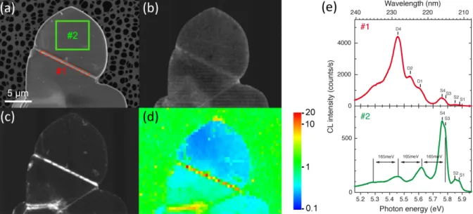
Such studies are now possible thanks to the recent development of dedicated photoluminescence (PL) and cathodoluminescence (CL) experiments running at 4K and adapted to the detection in the far UV range (up to 6eV) [1]. We can also combine various TEM techniques and CL experiments in a FEG-SEM with a spatial resolution of 3nm on the same nano-object. With these tools, we investigated the structure and luminescence of various structures, from high quality crystals [2], exfoliated nanosheets to multi-wall nanotubes [3]. As a result, BN materials present original optical properties, governed by excitonic effects in the 5.5–6eV energy range. Two kinds of excitonic luminescence have been identified and are called S and D lines [4]. As revealed from CL-TEM analyses, D lines are issued from defective areas (Fig 1), so that D/S ratio can be used as a qualification parameter of the defect densitiy [5]. This procedure has been applied to understand the first luminescence studies of few layers individual BN flakes [5].
Concerning nanotubes, CL images reveal that the luminescence in the 5.5–6eV energy range is strongly inhomogenous and oscillating. Thanks to a deep investigation combining different TEM techniques, we have shown that the tubes display a complex twisted faceted structure and that the twist period is correlated with the luminescence oscillations (Fig 2). Furthermore, we could show that excitons, responsible for the spectacular localization of the luminescence, are trapped to specific defects, twisted along with the faceting structure.
Finally, low-loss EELS providing an alternative approach to the nature of electronic excitations [6], we will show how it is an efficient tool to investigate the local structure and optical properties with an energy resolution below 100meV of different BN layers and nanotubes.
[1] P. Jaffrennou et al., PRB 77 (2008) 235422
[2] T. Taniguchi et al., J. Cryst. Growth 303 (2007) 525 [3] C. Tang et al., Chem. Commun. 12 (2002) 1290 [4] K. Watanabe et al., PRB 79 (2009) 193104 [5] A. Pierret et al., PRB 89 (2014) 035414 [6] R. Arenal et al., PRL 95 (2005) 127601
Acknowledgement: The research leading to these results has received funding from the European Union Seventh Framework Programme under grant agreement n°604391 Graphene Flagship. D. Golberg, T. Taniguchi and K. Watanabe from NIMS Japan are warmly acknowledged for providing samples.
Fig. 1: (a) SEM image of a h-BN crystallite; (b), (c) Corresponding CL images recorded (b) on the main S line (S3-S4), and (c) on the main D line (D4). (d) Map of the D/S ratio. (e) CL spectra recorded in the areas #1 (grain boundary) and #2 (middle of the grain), indicated in (a).
Fig. 2: Images of a BN nanotube: (a) 3nm spatially resolved CL image recorded at 5.49 eV (226 nm); (b), (c) Corresponding TEM images in (b) bright-field mode, and (c) dark-field mode on the (100) reflection. (d) Heptagonal tube cross-section obtained by tomography experiment. (e) Structure of the tube as deduced from (b-d) images.