HAL Id: tel-01198671
https://tel.archives-ouvertes.fr/tel-01198671
Submitted on 14 Sep 2015HAL is a multi-disciplinary open access archive for the deposit and dissemination of sci-entific research documents, whether they are
pub-L’archive ouverte pluridisciplinaire HAL, est destinée au dépôt et à la diffusion de documents scientifiques de niveau recherche, publiés ou non,
New antenna for millimetre wave radar
Muhammad Nazrol Bin Zawawi
To cite this version:
Muhammad Nazrol Bin Zawawi. New antenna for millimetre wave radar. Other. Université Nice Sophia Antipolis, 2015. English. �NNT : 2015NICE4017�. �tel-01198671�
UNIVERSITE NICE SOPHIA ANTIPOLIS
ECOLE DOCTORALE STIC
SCIENCES ET TECHNOLOGIES DE L’INFORMATION ET DE LA COMMUNICATION
T H E S E
pour l’obtention du grade de
Docteur en Sciences
de l’Université Nice Sophia Antipolis
Mention :
Électronique
présentée et soutenue par
Muhammad Nazrol BIN ZAWAWI
New Antenna for Millimetre Wave Radar
Thèse dirigée par Claire MIGLIACCIO
soutenue le (jour mois année)
Jury :
Mauro ETTORRE HDR, CR1-CNRS, IETR UMR 6164, Rapporteur
Université de Rennes 1
Acknowledgments
Foremost, I would like to express my sincere gratitude to my supervisor, Claire Migliaccio for her continuous support in my study and research. Her patience, motivation, enthusiasm and immense knowledge had greatly influenced me. Her guidance helped me in all the time of research and writing of this study. I could not have imagined having a better supervisor for my electronic path study and my academic career progress.
Besides my supervisor, I would like to thank my assistant supervisor Jerome Lanteri for his idea, views and technical knowledge in RF field. Not to forget my classmate and officemate Philippe Perissol for his great help. My sincere thanks also go to all lecturers in Electronic Department of University Nice Sophia Antipolis, Christian Pichot, Jean Yves Dauvignac, Geoges Kossiavas and Jean Marc Ribero for their professional support and knowledge during my academic studies.
I am greatly indebted to Lutfi Arif Bin Ngah and Raja Fazliza Binti Raja Suleiman for their stimulating discussions, great opinions, insightful comments and guidance in writing. I also would like to thank my fellow batch mates and the rest of colleagues in LEAT.
Last but not least, I am eternally indebted to my beloved mother and the rest of my family members for their spiritually endless support.
Contents
1. Introduction 1 2. Bibliography 3 2.1. Overview . . . 3 2.2. Introduction to reflectarray . . . 4 2.2.1. History . . . 4 2.2.2. Main components . . . 4 2.2.3. Working principle . . . 7 2.2.4. Phase-shift distribution . . . 10 2.2.5. Beam scanning . . . 132.2.5.1. 2x2 antenna array using Butler matrix . . . 13
2.2.5.2. Focal plane array based on microfluid . . . 16
2.2.5.3. Reflectarray with single bit phase shifter . . . 18
2.2.6. Advantages & Disadvantages . . . 20
2.3. Elementary cell . . . 21
2.3.1. Single layer . . . 21
2.3.2. Multi layer . . . 22
2.4. Active Reflectarray . . . 24
2.4.1. Active elementary cell . . . 24
2.4.2. RF MEMS . . . 25 2.4.3. Varicap diode . . . 27 2.4.4. Liquid Crystal . . . 30 2.4.5. Ferroelectric . . . 33 2.4.6. PIN diode . . . 35 2.5. Fresnel Reflectarray . . . 37 2.6. Application . . . 39 2.7. Conclusion . . . 39 3. Reflectarray modelisation 41 3.1. Theoretical analysis . . . 42 3.2. Parameters definitions . . . 45 3.3. Directivity calculation . . . 48
3.3.1. Power received at the elementary cell . . . 48
3.3.2. Incident wave at the elementary cell . . . 48
3.3.3. Reflected wave at the elementary cell . . . 49
Contents Contents
3.3.5. Power density and directivity . . . 54
3.4. Simulation program . . . 55
3.4.1. Functionalities . . . 56
3.4.1.1. Feed gain radiation pattern file . . . 57
3.4.1.2. Reflection coefficient (S11) file for passive reflectarray 57 3.4.2. Ansoft HFSS elementary cell simulation model . . . 58
3.4.3. Environment and structure . . . 61
3.5. Simulation analysis . . . 62
3.5.1. Results comparison . . . 64
3.5.2. Order of the phase correction . . . 68
3.6. Conclusion . . . 72
4. Active fresnel reflectarray (AFR) 73 4.1. Elementary cell design . . . 73
4.1.1. Passive cell . . . 74
4.1.2. Frequency adaptation . . . 76
4.1.3. Diode integration . . . 82
4.1.4. The diode DC polarization circuit . . . 87
4.1.5. Dieletric standardization using RT/duroid® 6002 . . . 94
4.1.6. Dieletric standardization using Meteorwave™ 2000 . . . 107
4.2. Reflectarray simulations . . . 122
4.2.1. Optimal frequency of the AFR . . . 122
4.2.2. Beam scanning capability . . . 130
4.2.3. Result comparison against CST . . . 133
4.2.4. Improvement using optimized elementary cell design . . . 135
4.3. Conclusion . . . 138
5. Diode controller 139 5.1. Circuit conception . . . 139
5.2. Working mechanism . . . 142
5.3. Components . . . 143
5.3.1. Micro-controller (Arduino board) . . . 145
5.3.2. Matrix sub-circuit . . . 146
5.3.2.1. Serial to parallel output circuit . . . 149
5.3.2.2. Digital to analog switch circuit . . . 153
5.4. Test and validation . . . 156
5.5. Conclusion . . . 161
6. General conclusion 163
7. Resume (French) 165
A. Object oriented programming in Matlab 167
Contents 1 8 1 s n o i t a c i l b u P 3 8 1 e a t i V m u l u c i r r u C
1. Introduction
This project has been conducted in Laboratoire d’Electronique, Antennes et Télécommunications (LEAT) in Sophia Antipolis and is funded by Universiti Malaysia Pahang (UMP) under the doctorate grant awarded by the Ministry of Education Malaysia (MOE). The supervisor for this project is Claire Migliaccio (Professor at University Nice Sophia Antipolis) and assisted by Jerome Lanteri (Associate profes-sor at University Nice Sophia Antipolis).
The objective of this project is to design and fabricate a reconfigurable re-flectarray with beam scanning capability at 20 GHz for unmanned aerial system (UAS) communication link where this antenna will be used to transfer the radar measurements to the satellite in real time. Reflectarray is a type of antenna that shares similar functionality to parabolic reflector antenna. The main difference is the physical and geometry appearance of the antenna where reflectarray has flat reflecting panel instead of parabolic reflector. The reflecting panel consists of ele-mentary cell which is used to control the reflected phase of the incident wave. By controlling the reflected phase on each elementary cell, the radiation pattern of the antenna can be focused to any desired direction.
The integration of the phase control mechanism in the elementary cell is the main challenge that needs to be solved and studied. This consists of understand-ing the theory of the reflectarray, designunderstand-ing the reconfigurable elementary cell with optimum performance and cost effective material, evaluating the reflecatrray per-formance and integrating the phase control system.
This manuscript is written in 4 main chapters. The first chapter discusses the introduction of the reflectarray, the beam scanning working principle and the latest technologies existing to create a reconfigurable reflectarray. This chapter also presents the chosen technology and discusses the main reason behind the choice.
The second chapter is about the reflecarray theory and the different calculations to produce radiation pattern of the reflectarray. These calculations are used to create in house reflectarray simulator in order to help and to accelerate the design process of the active reflectarray.
In third chapter the process of designing a reconfigurable elementary cell is discussed and explained. Material comparison is made to evaluate the improve-ment over the reflectarray performance. Simulation results are shown in order to demonstrate the beam scanning capability achieved using the active cell.
Chapter 1 Introduction The final chapter shows the work realized for the diode controller part which is used to steer the focused beam direction. This includes the simulation, fabri-cation and validation of the diode controller circuit using LED panel matrix that represented the phase distribution of the reflectarray.
General conclusion is made in in the end of the fourth chapter. The overview of the project completion and the possible improvement for the future work are discussed in this section.
2. Bibliography
2.1. Overview
Antenna is the critical part in any wireless communication system, where an-tenna is functioning as the main entrance or departure point in signal reception and transmission. This main point needs to be optimized and carefully designed in order to ensure the functionality of the communication system. There are many types of antennas in different physical forms and technologies for different types of applica-tions. Recently, radar application has been identified as an important application in security and imaging fields, especially in aviation industry.
Radar application requires antenna with high directivity and low secondary lobes. In this application, antenna array is among of the good candidates. By combining small unit of antenna into arrays, the directivity of the antenna can be increased and there is possibility to control the focused beam direction. Antenna array uses microstrip lines to feed the antenna unit. As the size of the array increases, the design of the feed lines will be more complicated and this will increase the loss in the feed transmission lines. To overcome these problems, the transmission lines can be replaced by optical transmission. This is similar to parabolic reflector antenna, which uses optical feed as the primary source. In this category, antenna is able to function based either on transmission or reflection method. When the method chosen is based on the transmission, the antenna is known as “transmitarray” and when the method is based on the reflection, the antenna is known as “reflectarray”. Both methods share the same designs complexities, which reside in the design of the unit cell or known as the elementary cell. To create a large antenna, the same unit cells designs are combined together. This simplifies the process to create and design passive or active antenna because the same units cell design is repeated for the whole structure. [1] is the recent examples of the reflectarray designed for radar application. The reflectarray functions at 120 GHz and has been designed to enable active phase shifter integration to achieve electronic beam scanning capability.
Beside radar application, there are recent applications which function above 100 GHz and at sub-millimeter wavelengths, such as earth observation, imaging system, and molecular spectroscopy [2, 3, 4, 5] that require reconfigurable reflectarray. Such requirements have created interest among researchers and engineers to design active reflectarray and create new different technologies for controllable reflectarray. This includes MEMS [6], non-linear material such as Ferroelectric films [7] and liquid crystals [8].
Chapter 2 Bibliography
2.2. Introduction to reflectarray
The reflectarray antenna consists of a flat reflecting surface and an illuminating feed antenna called primary source, which is usually placed in the center of the reflecting surface.
2.2.1. History
The concept of the reflectarray was realized by Berry, Malech, and Kennedy [9] in early 1960s. At that time, the design of the reflectarray was bulky and heavy due to the use of low frequencies for most of wireless operations. There was no reflecting panel and short-ended waveguide elements with variable-length were used to compensate the incident wave delay. By determining the appropriate length of the individual waveguide elements, the desired radiation pattern could be formed in the far field region.
In the end of 1970s, the printable microstrip antennas technology was intro-duced. This encouraged researchers to study the possibility of combining reflectar-ray concept with the microstrip technology which had produced the first reflectarreflectar-ray based on microstrip elements in 1978 by Malagisi [10]. As the printable microstrip became more accessible in the end of 1980s, many microstrip based reflectarrays had been developed with the purpose to have lighter and smaller reflectarrays. Starting from 1990s, attempts had been made to produce active reflectarray and in 1996, 94 GHz 1-bit monolithic reflectarray fabricated on a single wafer was introduced in Phased Array Conference and was capable to do wide-angle (±45°) electronic beam scanning [11].
2.2.2. Main components
In Fig. 2.1, the image on the left shows the side view of the reflectarray con-figuration while image on the right shows the real concon-figuration of the fabricated reflectarray using microstrip rectangle patches as the radiating elements. The feed is positioned in the center of the reflecting panel with a fixed distance from the panel. This distance is noted as f in the side view image and is known as focal distance. The distance is usually expressed in the ratio of f /D where D is the dimension of the reflecting panel.
It is possible to place the feed in a different position than the middle as shown as in Fig. 2.2. The reflectarray [12] uses an offset feed to avoid the aperture blockage problem and a special prolate feed to improve the maximum gain level and to have very low side lobe level. Another alternative to minimize the aperture blockage effect is by using dipole arrays to replace conventional horn antenna as demonstrated in [13]. In the paper, a broadband printed log-periodic dipole arrays (PLPDA) is used to replace the horn antenna.
2.2 Introduction to reflectarray
Figure 2.1.: Reflectarray components configuration
To form a reflecting surface, there are many types of radiating elements that can be used such as printed micro strip patches [14, 15], open-ended waveguide, dipole [16] or rings [17]. These elements are known as elementary cells. The most common element found in literature is the radiating element based on micro strip patches. There are many shapes [18, 19] and structure variations for the micro strip based elementary cell. Fig. 2.3 and Fig. 2.4 show two different shapes of the radiating element based on fractal and dual split-loop shape respectively. The design of the elementary cell plays very important role in order to optimize the reflectarray performance. More information on the elementary cell will be discussed in sec. 2.3.
Chapter 2 Bibliography
Figure 2.3.: Fractal shape elementary cell (From [18], © 2012 IEEE.)
2.2 Introduction to reflectarray
2.2.3. Working principle
Reflectarray is designed to produce a planar phase front in the far-field region when the feed is positioned at its focal point. It uses the same working principle as the parabolic reflector. In case of the parabolic reflector, it is its unique parabola geometry which forms and reflects the planar phase front as illustrated in Fig. 2.5. The total paths of the rays are represented by the blue and the red lines and show that both of them are parallel and have the same length from the feed. In this case, the rays are said to be collimated. This enables the field on the focal plane to be in phase and travel in the same direction which results in a high directional radiation pattern in the far-field region. Example of parabolic reflector antenna or also known as dish antenna is shown in Fig. 2.6.
Figure 2.5.: Parabolic reflector configuration
In case of reflectarray, the parabola reflector is replaced with the reflecting panel composed with elementary cells as in Fig. 2.7. Due to the absence of parabola reflector, the rays will reach the reflecting panel with some delays and without any correction applied, the reflected rays are not anymore parallel and in phase. To overcome the problem, the phase of each elementary cell on the reflecting surface is adjusted to compensate the delays.
In Fig. 2.7, the elementary cell EC1 phase (Ï1) is adjusted to correct the delay for trajectory d1 and the elementary cell EC2 phase (Ï2) is adjusted to compensate the delay for trajectory d2. By assigning the correct phase values for each elementary
Chapter 2 Bibliography
Figure 2.6.: Parabolic reflector antennas used as part of Atacama Large Millimeter Array (ALMA) antennas (© ALMA (ESO/NAOJ/NRAO), W. Garnier (ALMA)) cell, the delay of the incident field can be corrected so that the reflected field will be able to form a planar phase front in the far-field region.
Each elementary cell needs to have different phase values to correctly com-pensate the delay. The phase value is directly related to the cell position on the reflecting panel, its distance from the feed and the reflected focused beam direction. Typical reflectarray is designed to collimate the main beam at Ï = 0° and ◊ = 0° in spherical coordinates as shown in Fig. 2.8. At this direction, the phase for each elementary cell can be obtained using 2.1.
Ïn = 360
c × f × dn (2.1)
c : speed of light
f : working frequency
dn : distance between the elementary cell and the feed
The farthest elementary cell will have the biggest phase compared to the ele-mentary cell located in the center of the reflecting panel.
2.2 Introduction to reflectarray
Figure 2.7.: Reflectarray phase compensation
Chapter 2 Bibliography
2.2.4. Phase-shift distribution
Equation 2.1 assumes that the elementary cell arrangement is in one dimension (1D) as illustrated in Fig. 2.7. In reality, the arrangement of the elementary cell on the reflecting panel is in two dimensions (2D) where m represents cell column and
n represents cell row. The equation can be rewritten as :
Ïmn = 360
c × f × dmn (2.2)
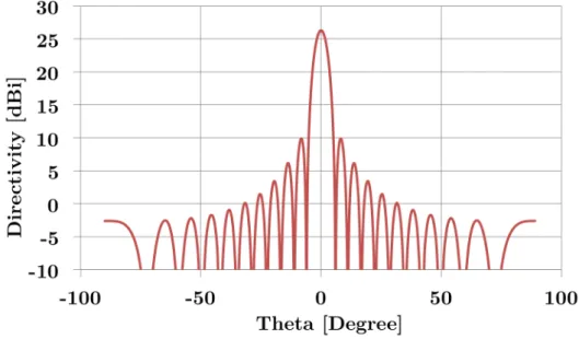
The two dimensions phase values arrangement will create a phase pattern known as phase-shift distribution for certain reflectarray’s size in terms of elementary cell’s column (x axis) and row (y axis). Fig. 2.9 shows the phase-shift distribution for 21 × 21 elementary cells when the main beam is collimated at Ï = 0° and ◊ = 0° at 20 GHz. This phase-shift distribution will produce a radiation as shown in Fig. 2.10.
Figure 2.9.: Phase-shift distribution for 21 × 21 elementary cells reflectarray at 20
2.2 Introduction to reflectarray
Figure 2.10.: Reflectarray’s radiation pattern when using phase-shift distribution shown in Fig. 2.9
The equation 2.2 has been simplified from its original equation 2.3 [20] to show that the compensated phase varies linearly with the elementary cell’s distance from the feed. This observation is important in order to understand the phase correction influence on the reflectarray performance such as the bandwidth and maximum directivity level.
Ïmn= k0(dmn− (xmncos Ïb + ymnsin Ïb) sin ◊b) (2.3) In equation 2.3, the direction of the collimated beam is represented by Ïband ◊b. The position of the elementary cells in cartesian coordinate is specified with xmnand
ymn. k0 is the propagation constant in vacuum. When modifying the focused beam direction, the phase values for each cell will be also changed. This will generate a new phase distribution pattern as shown in Fig. 2.11. The new pattern shows some phase value offset in x axis direction which indicates that the main beam is not anymore at 0° but has changed to a new direction. This also can be seen on the new radiation pattern in Fig. 2.12 where the main beam direction is now focused at 20°.
This concludes that the radiation pattern can be changed by modifying the phase-shift distribution. In this case, the main beam direction can be varied by using some specific phase distribution patterns such as shown in Fig. 2.11. This can be directly applied to the reflectarray in order to achieve electronic beam-scanning capability.
Chapter 2 Bibliography
Figure 2.11.: Phase-shift distribution for 21×21 elementary cells reflectarray
func-tions at 20 GHz with f/D = 0.5 and main beam direction is focused at Ïb = 0° and ◊b = 20°
Figure 2.12.: Reflectarray radiation pattern when using phase-shift distribution focused at Ïb = 0° and ◊b = 20° . Working frequency is 20 GHz and f/D = 0.5
2.2 Introduction to reflectarray
2.2.5. Beam scanning
Beam scanning is the capability to change the focused beam direction in a specified range of angles. This capability is essential in radar application and in imaging system such as in medical field in order to detect and determine objects. Beam scanning can be achieved either mechanically or electronically. This section will describe 3 examples of antenna designs with beam scanning capability. The first example uses integrated waveguide phase shifter. The second example is focal plane array (FPA) based on microfluid [21]. The third example will show reflectarray functioning at 60 GHz and uses p-i-n diode as electronic phase shifter. These 3 examples are chosen to show different techniques can be used to do beam scanning.
2.2.5.1. 2x2 antenna array using Butler matrix
In [22], the beam scanning is achieved by using subtrate integrated waveguide (SIW) phase shifter. The antenna is designed for Ka-Band application and it is capable to do two-dimensional beam scanning. The phyical design of this antenna consists of 2 × 2 antenna array. The single antenna element has 3 layers as shown in Fig. 2.13. The main feed (SIW) is implemented directly into the layer 1 which uses high permittivity Rogers RT/Duroid 6010 (Ár = 10.5, tan ” = 0.0023@10GHz) as substrate material. Chosen material for layer 2 is Rohacell 31 IG/A (Ár = 1.05, tan ” = [email protected]) and the layer 3 material is Rogers ULTRALAM 3850 (Ár = 2.9, tan ” = 0.0025@10GHz). The radiating element which is the annular ring is printed on the top layer (layer 3).
4 single antenna elements are combined together to represent the Butler ma-trix which will be used to calculate the focused beam direction. The rectangular waveguide equivalent model for the proposed Butler matrix is shown in Fig. 2.14. Port P1, P2, P3 and P4 are the input feed ports while P5, P6, P7 and P8 are the output ports to feed the circular radiating element on the top layer via coupling. The beam scanning mechanism for this antenna can be analysed using the phase profile equation of the Butler matrix as shown in 2.4 and 2.5.
In these equations, „0 and ◊0 are the focused beam direction. „x and „y are the progressive phase shift in x and y direction. k is the propagation constant in the free space. dx and dy are the distances between two neighboring antenna element in x and y directions. The theorectical progressive phase between ports values are calculated using formula 2.4 and 2.5. Then the theoretical beam directions are obtained. The respective values are shown in the Tab. 2.1 and there are 4 possible focused beam directions.
Fig. 2.15 shows the fabricated antenna with 4 feed ports indicated by P1, P2, P3 and P4. To obtain one beam which focused at one of the four beam directions, only one respective feed port will be used. By changing the feed port, the antenna pattern radiation can be changed and focused to 4 diferent directions.
Chapter 2 Bibliography
Figure 2.13.: Single antenna element with integrated waveguide phase shifter (From [22], © 2014 IEEE.)
„x = −kdxsin(◊0) cos(„0) „y = −kdysin(◊0) sin(„0) (2.4)
„0 = tan−1(φφyxddxy) ◊0 = sin −1 Ú (φx kdx) 2+ (φy kdy) 2 (2.5) Port „0, Ï0 1 (21°,61°) 2 (-38°,-31°) 3 (-21°,61°) 4 (38°,-31°)
2.2 Introduction to reflectarray
Figure 2.14.: Rectangular waveguide equivalent model for 4x4 Butler matrix (From [22], © 2014 IEEE.)
Chapter 2 Bibliography
2.2.5.2. Focal plane array based on microfluid
In [21], the antenna structure is a multilayer structure that consists of 4 layers and is designed to function at Ka-Band (30 GHz) as shown in Fig. 2.16. This antenna is capable to do 1-D beam scanning by using metal liquid. The top layer has an 8 cm diameter extended hemispherical Rexolite (Ár = 2.56, tan ” = 0.0026) lens. On layers 2 and 3, there are interconnected microfluid reservoirs and channels fabricated by bonding polydimethyl-siloxane (PDMS) (Ár = 2.8, tan ” = 0.02) and liquid crystal polymer (LCP) (Ár = 2.9, tan ” = 0.0025) substrates. There is only a single antenna element in this structure which is a small volume of liquid-metal mercury (2.5µL,
‡ = 1 × 10⁶ S/m) residing inside a low-loss Fluorinert FC-77 solution (Ár = 1.9, tan ” = 0.0005). The combination of liquid-metal and Fluorinert solution is filled into microfluid reservoirs and channels. The feeding network is placed on the layer 4 which uses Rogers RT5880 (Ár = 2.2, tan ” = 0.0007).
Figure 2.16.: Focal plane array structure (From [21], © 2013 IEEE.)
Patch antenna is realized when the reservoir is filled with the liquid-metal and it will radiate using the coupling source coming from the feed network which is located below of the microfluid reservoir. Using this concept, the single patch antenna can be moved into any microfluid resevoir which will result in the changes of the pattern radiation direction. To move the liquid-metal into different reservoirs, a bi-directional micro pump is used as shown in Fig. 2.17. In total, there are 8 liquid reservoirs which will produce 8 different beam directions. These patches act as the feed to the lens and by changing the position of the feed (moving the liquid-metal), the direction of the beam is changed.
Fig. 2.18 shows the fabricated prototype in 3 different views. (a) shows the printed feed network, (b) shows the upper layer with hemispherical Rexolite 8-cm diameter lens and (c) shows the back view of the fabricated antenna. The measured performance of this antenna can be viewed in Fig. 2.19. From the result, the beam scanning capability is achieved by moving liquid-metal into different reservoirs, in this case, the liquid-metal is moved into reservoir #1, #2, #3 and #4.
2.2 Introduction to reflectarray
Figure 2.17.: Liquid-metal direction and movement concept (From [21], © 2013 IEEE.)
Figure 2.18.: Fabricated prototype of FPA (From [21], © 2013 IEEE.)
Figure 2.19.: Measured performance : (a) |S11| and (b) normalized gain (From [21], © 2013 IEEE.)
Chapter 2 Bibliography
2.2.5.3. Reflectarray with single bit phase shifter
In [23], the beam scanning capability is achieved by modifying the phase dis-tribution of the reflectarray as discussed in sec. 2.2.4. The elementary cell is a multilayer structure cell as shown in Fig. 2.20. The main radiating element (patch) is printed on the top layer (Layer 1) and this patch is connected to the segmented stub using p-i-n diode. The effective stub length depends on the diode state (ON or OFF) which produces 2 possible stub lengths.
Figure 2.20.: (left) Active multilayer elementary cell for 60 GHz single-bit reflec-tarray; (right) Fabricated reflectarray (From [23], © 2011 IEEE.)
This enables the elementary cell to have 2 different phase values with 180° of difference between them. These values can be controlled electronically using dedicated digital circuit in order to obtain the desired phase value as shown in Fig. 2.21.
Figure 2.21.: Reflection cofficient of the elementary cell using single bit phase shifter (From [23], © 2011 IEEE.)
2.2 Introduction to reflectarray
The cell is limited to correct only 2 phase values and this degrades the reflectar-ray performance because there is an increase of phase compensation error compared to passive reflectarray. In addition, the reflected power of the cell is decreased due to the high loss in PIN diode. The loss when the diode is biased (ON state) is high which is 5.3 dB and for OFF state the loss is 2.7 dB.
Therefore the size of the reflectarray needs to be increased which results in a total number of 160x160 (25600) elementary cells. The fabricated antenna is shown in Fig. 2.20 on the right side.
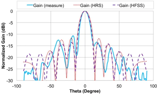
Fig. 2.22 shows the measured and simulated radiation patterns with the beam scanning capability for every 5 degrees. From this results, it shows that the simula-tion and measurement radiasimula-tion patterns are in good agreement.
Figure 2.22.: Radiation patterns for beam scanned every five degrees in (a) az-imuth and (b) elevation (From [23], © 2011 IEEE.)
This active reflectarray will be used as main primary reference and example in this work. More detail and information about this antenna will be discussed in the next following chapters, especially when discussing the active elementary cell’s design.
Chapter 2 Bibliography
2.2.6. Advantages & Disadvantages
Because reflectarray is the combination of reflector antenna and array antenna, it inherits its ancestor advantages such as a very good efficiency. This is true for a very large dimension of reflecting surface or aperture and since no power divider is used thus very little resistive insertion loss is encountered.
Another advantage of reflectarray is that the main beam can be tilted at large angle (>50°) from its broadside direction. It’s possible to integrate the electronic phase shifter into the elementary cells for wide-angle electronic beam scanning. With this capability, the complicated high-loss beam forming network and high-cost trans-mit/receive (T/R) amplifier modules of a conventional phased array are no longer needed.
The reflectarray technology can be applied throughout the microwave spectrum, as well as at the millimeter - wave frequencies. So, when working in the millimeter wave spectrum, the size of the antenna could be reduced to a smaller size while maintaining the gain.
On the other hand, working in this spectrum will also allow us to have a larger bandwidth, because there are more spectrum available at the high frequencies com-pared to lower frequencies (< 5 GHz).
The reflecting surface is usually fabricated using micro strip patches technol-ogy. Using this technology, the process is simpler and inexpensive especially when produced in large quantities. Thus, the fabrication cost can be reduced while com-promising its quality.
One disadvantage of reflectarray is its bandwidth’s limitation. Generally, the bandwidth can’t exceed 10% and it depends on its elementary cells design, focal length and aperture size. Compared to parabolic reflector, which is theoretically having an infinite bandwidth, reflectarray has a narrow bandwidth. Many researches have been conducted to tackle this limitation.
2.3 Elementary cell
2.3. Elementary cell
Elementary cell is the primary component in a reflectarray and plays an impor-tant role to correct the incident wave delay. As discussed previously in sec. 2.2.5, there are many types of elementary cell designs and the main objective of these designs is to produce the correct or the desired reflected wave phase value. The designs can be categorized into a single layer design elementary cell or multi layer elementary cell.[20]
2.3.1. Single layer
Single layer elementary cell is a simple design which consists of a printed radiat-ing elements and a ground metal on a sradiat-ingle piece of substrate as shown in Fig. 2.23. This type of design is easy to be fabricated using microstrip technology and inexpen-sive in term of fabrication’s cost. In this design, the phase of reflected wave depends on the radiating element shape design, position and rotation angle. By varying these three characteristics, the desire phase value can be obtained. An inconvenient of this design is that the various combinations are limited to the elementary cell space, which will result in limited number of possible phase values.
Figure 2.23.: Single layer elementary cell design structure
For rectangular shape radiating element or rectangular patch, the reflected phase can be varied by changing the width and height of the patch [24, 25, 26]. Without changing the patch dimension, it is possible to control the reflected phase by attaching the stub with different lengths to the main patch [27]. In this case, the phase value will depend on the length of the stub. There is also elementary cell design which manipulates radiating element rotation angle to control the phase such as in [28].Using these techniques, the maximum range of phase variation can not exceed 360°. The phase variation versus the variable length or width is strongly non-linear due to the narrow band nature of microstrip patch which is in general about 3%. The phase variations are very sensitive to the frequency or patch di-mension variations which will limit the working bandwidth of the reflectarray. To
Chapter 2 Bibliography overcome and improve the reflectarray bandwidth, techniques such as using thicker substrates, stacking multiples patches and using rotated subarray elements have proven to work and 15% of bandwidth improvement has been reported [29].
2.3.2. Multi layer
Multi layer elementary cells consists of multiple layers of substrates stack to-gether and is able to produce larger phase variations than single layer elementary cell which is in several times of 360°. In [30], two layers are stacked together as a single unit elementary cell as shown in Fig. 2.24. This design allows the phase variation to be smoother and cover phase values larger than 360°. The thickness of the substrates for each layer can be increased to obtain smooth and more linear phase variation without reducing the phase range values to be less than 300°.
Figure 2.24.: Two layer elementary cell design (From [30], © 2001 IEEE.) The second multi layer design uses elements separations in the structure and works based on the coupling effect between each element [31, 32, 30, 33]. Fig. 2.25 shows the aperture-coupled patches elementary cell design. In this design, there is a clear separation between radiating element and the phase tuning stubs which controls the reflected phase values. The radiating element which is the rectangular patch is separated from the stub by the aperture layer. The phase value can be controlled by adjusting the stubs length and can be folded to obtain very large value of phase variation. To obtain smoother phase variation, the thickness of d(1) can be increased and the size of rectangle aperture can be adjusted.
The multi layer elementary cell design is more complex. This will increase the fabrication complexity and cost. However, this type of structure is more interesting as many possibilities exist to extend the elementary cell behaviour such as the inte-gration of active and electronic components to produce active elementary cell. The separation of the elements in aperture-coupled patches elementary cell design has some clear advantages over the single layer design. The phase tuning stub is placed
2.3 Elementary cell
Figure 2.25.: Elementary cell based on a U-shaped aperture-coupled delay line (a) Expanded view, (b) top view (From [31], © 2006 IEEE.)
on a separate layer and this will ensure plenty of space left for increasing the stub length, plus the stub length can be folded to fill up the space. Electronic element like diode can be integrated on the phase tuning stub layer without affecting the radiating layer on the top of the cell. The radiating layer itself is very sensitive to any fabrication error or any presence of unwanted physical object which contributes to reflected phase value error.
Chapter 2 Bibliography
2.4. Active Reflectarray
Passive reflectarray has been proven working well and has been widely used in telecommunication and RADAR applications due to its nature of having high gain and good efficiency. There is a significant growth of RADAR application in security field especially in car safety systems in order to prevent and avoid collisions. This requires an intelligent detection system to ensure that the passengers are well protected and safe. One of the most important part in the system is the antenna which emits and receives signals. Passive reflectarray is the suitable candidate for this type of application because its physical design is compact and small at higher frequencies and has been used as the antenna for such system [34, 35, 36].
To improve modern detection systems, the reflectarray needs to evolve to be-come intelligent and reconfigurable from passive to active reflectarray. Because of this, the demands for electronic beam scanning capability and radiation pattern con-figurability are identified as an important challenge for on-going applications and they can be defined as important capabilities for an active reflectarray.
2.4.1. Active elementary cell
Active reflectarray uses the same components as the passive reflectarray, but new components are added to the passive’s structure. In the elementary cell, elec-tronic phase-shifter is integrated inside the cell design to have the total control of the reflected phase. Additional controller circuit is required to handle a large quantity of electronic phase-shifter inside the elementary cells.
There are variety of technologies that can be used as the phase-shifter in active elementary cell. Each of these technologies has its own benefits and disadvantages especially in term of cost, fabrication complexity, control complexity, losses and power consumption.
2.4 Active Reflectarray
2.4.2. RF MEMS
MEMS stands for Microelectromechanical systems and in terms of the phase-shifter it can be considered as mechanical switch at a small scale. MEMS switch operates using mechanical structure thus offering some benefits to have null current consumption, good power efficiency, high isolation and low losses. Demonstration and proof of concept using MEMS switch have been made in [37, 38]. In [37], the elementary cell is made of two patches coupled through slots to microstrip-lines, which are connected to a common stubs as shown in Fig. 2.26. This cell is designed to function between 9.40 GHz and 11.40 GHz. The proposed elementary cell design is similar to the passive design discussed previously in sec. 2.3.2. Depending on the MEMS actuation voltage, the switch is either in ON or OFF state, and the phase tuning stub length varies producing two possible values of reflected phase.
Figure 2.26.: Reconfigurable double aperture-coupled delay line elementary cell based on MEMS switch (From [37], © 2011 IEEE.)
Fig. 2.27 shows the MEMS switch schematic. The switch will either join or disconnect the two segments of the phase tuning stub. This can be achieved when a biasing voltage of 25 V is applied between the electrodes and the ground plane. The silicon nitride membrane will be pulled down and touches the signal metal connector which is located between two ground connectors. This produces a short circuit that will join the two segments of the phase tuning stub. The simulated and measured reflected phase values are shows in Fig. 2.28 with phase difference between ON and OFF states is about 300°.
Chapter 2 Bibliography
Figure 2.27.: Schematic stack of the ohmic electrostatic MEMS switch (From [37], © 2011 IEEE.)
Figure 2.28.: Comparison between the measured and simulated reflected phase in the waveguide simulator for both states: OFF and ON (From [37], © 2011 IEEE.) In total, a MEMS switch in this design requires 8 wires to be functional. They are 2 wires for the DC voltage biasing, 4 wires for the via holes connected to the ground of the coplanar line and 2 wires for the RF signal between each segment of the phase tuning stub. Although MEMS switch can provide low losses of reflected wave, the process to integrate this switch is complex because of multiples connectors are required for each switch. In term of fabrication cost, this will be expensive because there are many switches need to be integrated for a complete reflectarray. In [6], difficulties to fabricate large MEMS array with independent voltage control has been reported.
2.4 Active Reflectarray
2.4.3. Varicap diode
Varicap diode is a type of diode whose capacitance varies as a function of the voltage applied across its anode and cathode terminals. In case of active elementary cell, varicap diode can be used as active element to control and modify the reflected phase electronically by varying the bias voltage. Delft University of Technology [39] has designed an electronic steerable reflectarray with integrates varicap diode and functions at 6 GHz. The elementary cell structure is a single layer structure with ground plane at the bottom layer. The radiating patch on the top is similar to rectangular patch but with some holes in the center of the patch (Hollow patch) as shown in Fig. 2.29.
Figure 2.29.: Geometry of a hollow patch loaded with varicap diode (From [39], © 2009 IEEE.)
The center part of the hollow patch primarily consists of varactor chip con-nected to the bias and ground signal microstrips lines. The varactor chip has been designed and developed at DIMES (Delft Institute for Micro-Electronics and Sub-microntechnology) and acts as tunable capacitive device [40, 41]. The chip has 5 connections and it is connected to the patch laminate using bondwires. The con-nection signal of bias and ground are brought from the bottom layer. This requires two additional vias (white circle) to bring those connectors to the top layer. Points A and B are the connections for the RF path and this path will have capacitance variation which depends on the varactor chip applied bias voltage.
To modify the reflected phase value, the capacitance value of the varactor is varied using a bias voltage between -12 V and 0 V. The reflected phase values versus capacitance values are shown in Fig. 2.30. Maximum phase variation obtained using
Chapter 2 Bibliography the varactor chip is about 250°. At f = 5.8 GHz the phase variation are small and at f = 6.2 GHz the variation is too steep. This shows that the reflectarray has a narrow bandwidth.
Figure 2.30.: Phase diagram of a hollow patch loaded with tunable varactor as function of capacitance (From [39], © 2009 IEEE.)
The fabricated reflectarray is shown in Fig. 2.31 with 6×6 elementary cells. The substrate used is Taconic TLX-0-0620-C1/C1 with a thickness of 1.57 mm and dielectric permittivity of Ár = 2.45. The connections to control the varactor chips are made from the bottom layer (back view) where each elementary cell can be controlled individually. In total there are 36 wires for biasing voltage purpose (yellow wire) and 6 wires as ground connector. Each column of the reflectarray requires one wire for grounding.
The biasing control is realized via PC and PCI-766 DAC (Digital-to-Analog converter). The DAC chosen has 16 channels with 16-bit resolution. Because there are only 16 channels available as output, the total 36 elementary cells biasing control is not possible to be done individually. The measured E-plane radiation patterns are shown in Fig. 2.32 and shows the reflectarray beam scanning capability between -15° and 15° at f = 6.15 GHz.
Using varicap diode is an interesting solution to have an active elementary cell but in term of the losses of reflected wave magnitude, varicap diode contributes to high losses of reflected wave magnitude which can degrades the overall reflectar-ray performance. In addition, the cost to fabricate reflectarreflectar-ray using this diode is expensive.
2.4 Active Reflectarray
Figure 2.31.: Manufactured active antennas: (a) front view; (b) back view. (From [39], © 2009 IEEE.)
Figure 2.32.: Measured radiation pattern of the active hollow MRA at 6.15 GHz (From [39], © 2009 IEEE.)
Chapter 2 Bibliography
2.4.4. Liquid Crystal
One interesting property of liquid crystal is the ability to change its mate-rial permittivity when quasi-static electric field is applied. This property can be exploited to produce a reconfigurable reflectarray. Several active elementary cell examples based on the liquid crystal have been demonstrated in [42, 43, 44].
In [44], the elementary cell structure is similar to single layer structure as shown in Fig. 2.33 and designed to function at 102 GHz. The radiating element is a rect-angular patch with bias line in the middle. The substrate between the patch and ground is a liquid crystal film with the thickness of 15 µm. The size of the patch is wp = lp = 0.77 mm and dimension of the elementary cell is Dx = Dy = 0.9 mm. The ground material chosen is copper coated with Si to satisfy mechanical requirement. The selected wafer surface [45] which is Quartz material (Ár = 2.56, tan ” = 0.0026) is placed on the top, above the patch to align the director of the liquid crystal molecules in the direction of the wafer surface as shown in the Fig. 2.33 in case of 0 V. Without this surface, the director of a liquid crystal is free to point in any direction.
Figure 2.33.: Structure of an elementary cell based on liquid crystal in [44] (From [44], © 2008 IEEE.)
Without any voltage applied between the bias line and ground (0 V), the di-rector of the liquid crystal molecules are aligned in the same direction of the quartz surface. In this case the permittivity is considered as Á⊥. When 10V of bias voltage is applied, the director of the liquid crystal molecules are oriented perpendicular to the wafer surface which results in a new permittivity value noted as Á!. This permittivity difference will affect the reflected phase values [46] and in this case, there are 2 possible of phase values, one corresponds for 0 V (Normal state) and the another one corresponds to 10 V (Biased state).
2.4 Active Reflectarray
Using the elementary cell design discussed previously, a reflectarray with ge-ometry shown in Fig. 2.34 is fabricated. The bias lines with the width of 50 µm are connected in columns to the metal pad which means the elementary cell in this design cannot be controlled individually. To do the measurement of the elementary cell in periodic environment, the same bias voltage is applied to all elementary cells simultaneously.
Figure 2.34.: Schematic plot of the reflectarray geometry (From [44], © 2008 IEEE.)
Fig. 2.35 shows the simulated and measured reflected magnitude and phase of the elementary cell. At f = 101.72 GHz, the phase difference between normal and biased state is 180°, therefore this frequency is chosen as the center design frequency for the reflectarray. The results show good agreement between the simulated and the measured one.
Designing and fabricating reconfigurable reflectarray using liquid crystal is still considered new and experimental. The cost to use the wafer as the director surface is considered to be expensive and not suitable for large reflectarrays. The difficulty to implement control system for each elementary cell is a challenging process with this technology. In recent work [47] shown in Fig. 2.36, the measurement of the reflectarray is performed at the elementary cell level without the measurement of the reconfigurable radiation patterns. To obtain the gain of the reflectarray, simulation using data from the measured elementary cell is mandatory.
Chapter 2 Bibliography
Figure 2.35.: Simulated and measured of reflection loss (upper), phase (lower) and phase agility (center) of liquid crystal based elementary cell (From [44], © 2008 IEEE.)
Figure 2.36.: Manufactured reconfigurable reflectarray in F-Band (From [47], © 2013 IEEE.)
2.4 Active Reflectarray
2.4.5. Ferroelectric
Ferroelectric based material is a type of material where the electrical polariza-tion can be changed by applicapolariza-tion of an external electric field [48, 49]. In microwave applications, ferroelectric material have been extensively studied as tuning elements such as tunable filters [50, 51], phase shifters [52] and matching networks. Barium-Strontium-Titanate or known as BST is the common ferroelectric material used and is commonly found in the literature.
In [53], the single layer structure is used as the elementary cell and is designed to function at 10 GHz. The size of the cell is 4.75 mm. The metallic patch is printed on the BST thick film and sintered on Al2O3 substrate (Ár = 9.80) with the thickness of 650 µm. The rectangular patch on the top acts as radiating element which is divided into two parts as shown in Fig. 2.37. The gap between the 2 parts is 13 µm. Fig. 2.38 shows the cross-section (from A and B) of elementary cell.
Figure 2.37.: Reconfigurable elementary cell with BST based varactor (From [53], © 2009 IEEE.)
The separation of the rectangular into 2 parts produces in a capacitively cou-pling between those parts. By applying an electrostatic field between the 2 rectangu-lar patches, the effective capacitance between them can be changed. This structure represents a BST varactor and it is implemented directly on the microstrip patch without any off-chip varactor.
The result of the elementary cell measurement is shown in Fig. 2.39. With a tuning field of 11.5 V/µm, a phase difference of 250° is obtained at 10.5 GHz. The introduction of the bias lines for the electric field has a considerable influence on the reflected wave, with additional 6 dB of losses and shifted resonance frequency.
Chapter 2 Bibliography
Figure 2.38.: Microscopic cross-section of a BST thick-film screen printed on top of Al2O3 substrate (From [53], © 2009 IEEE.)
Figure 2.39.: Reflected magnitude and phase for applied electrical field between 0 to 11.5V/µm (From [53], © 2009 IEEE.)
Utilizing BST thick-film as solution to achieve tunable elementary cell is inter-esting from the point of view cost and fabrication process. By using screen printing technique, an active elementary cell could be manufactured at a low cost. Plus, the ferroelectric based tunable components have higher tuning speed in picoseconds range [54]. Despite all these advantages, the ferroelectric based elementary cell needs high DC biased fields to obtain large phase-shift range and this will impose an inconvenient for a large size reflectarray. Plus, the process to design and imple-ment complete bias lines is also difficult and will result in poor performance of the elementary cell.
2.4 Active Reflectarray
2.4.6. PIN diode
PIN diode has been widely used as an electronic switch and it is often associated with phase tuning stub or delay line length variations [55, 56, 57, 58, 59]. In [59], the elementary structure is very similar to the one discussed in sec. 2.4.2 and functions between 10.1 GHz and 10.7 GHz. In this case, the RF MEMS switch is replaced by PIN diode and the bias lines are modified to fit in the diode switch. The expanded view of the elementary cell design is shown in Fig. 2.40.
Layer Material Ár tan” d4 Arlon 25N® 3.38 0.0025 bonder34 Eccobond 45® 3.40 0.0400 d3 Eccostock ® 1.12 0.0020 bonder23 Eccobond 45® 3.40 0.0400 d2 Arlon 25N® 3.38 0.0025 d1 Air 1.00 0.0002
Figure 2.40.: Expanded view of a reflectarray elementary cell based on aperture-coupled patches to a common tuning stub, using a PIN diode as electronic switch (From [59], © 2012 IEEE.)
The elementary cell concept is based on gathering two patches together as a single unit elementary cell. This enables the control of the two radiating patches to be done via a single PIN diode, thus reducing the diode usage and their associated DC biasing lines. The size of the unit is 36 mm × 18 mm and the size of the square patches as the radiating elements are 9 mm × 9 mm. The diode is modeled as capacitance in OFF state (reverse biasing) and as a resistance in ON state (forward biasing). The length of the phase tuning stub will be different and depends on the diode state. This will produce 2 different reflected phase values that will be used to change the phase-shift distribution.
The chosen PIN diode for this design is a GaAs MA4GP907 diode manufactured by MACOM and the diode characteristics are shown in Tab. 2.2. The simulated and measured results for the elementary cell are shown in Fig. 2.41. The required phase variations between 10.1 GHz and 10.7 GHz are about 150° to 200° and the loss is
Chapter 2 Bibliography around 4 dB. The loss by using PIN diode is higher than using RF MEMS switch.
Parameter Value Capacitance, CT 0.025 pF Series resistance, RS 4.2 W Forward voltage, VF 1.33 V Reverse voltage current, IR Max 10 mA
Table 2.2.: MA4GP907 diode electrical characteristics (From [59], © 2012 IEEE.)
Figure 2.41.: Measured and simulated reconfigurable elementary cell based on PIN diode reflected phase and magnitude (From [59], © 2012 IEEE.)
The reflectarray is designed to do 3 states beam scanning which are -5°, 0° and 5° and because of this, there is no need to control each individual elementary cell. Instead, they are controlled per row and this reduces the bias line design complexity. PIN diode technology is quite matured at the industry level. This means that diodes costs are not expensive and they have been extensively tested for various type of applications and conditions. The disadvantages of the PIN diode is that the loss is high especially when it is used at high frequencies and it will consume a lot of energy for large reflectarrays.
2.5 Fresnel Reflectarray
2.5. Fresnel Reflectarray
Reflectarray works by converting the spherical incident wave coming from the feed to a plane wave in the far-field region. Each of the elementary cell on the reflecting surface needs to have a correct phase value to compensate the incident wave delay associated to its travel’s distance, noted Dmn in Fig. 2.42. F is the focal length.
Figure 2.42.: Reflectarray side view
For Fresnel reflectarray, instead of correcting per elementary cell, the incident wave delay is compensated by zones known as Fresnel zone [60, 61]. The zone is defined by using the following equation 2.6.
rn = ˆ ı ı Ù2nF ⁄ P + A n⁄ P B2 (2.6)
The zone radius noted as rn is defined from the center of the reflectarray. n is the index of the zone and this value starts from 1. F is the focal length and l is the free-space wavelength. P is the order of correction desired. The phase correction of the zone is obtained from the equation 2.7.
Ïn= (n − 1)2fi
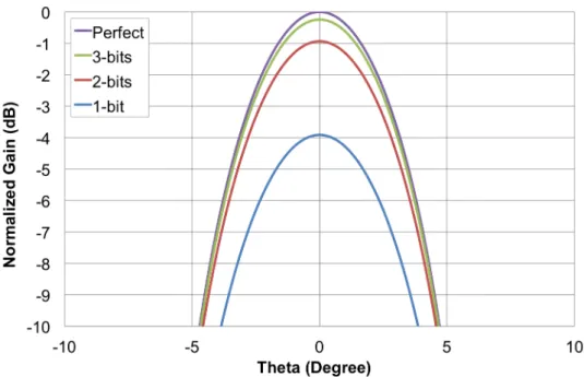
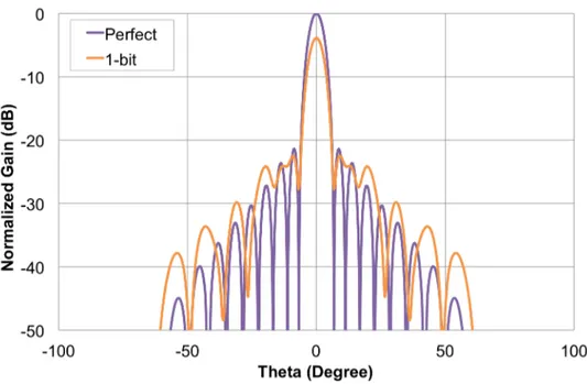
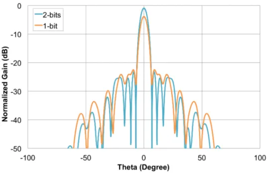
Chapter 2 Bibliography Theoretically, a large number of P will ensure better phase correction thus giving better reflectarray’s performance in term of maximum gain and lower side lobes levels. In reality, the chosen P value needs to reflect certain criterions such as the ease of manufacturing, design complexity and acceptable performance. The number of bit required depends on the P value and it determines the elementary cell design complexity.
Taking the example of P = 4, there are 4 possible phase values and this requires 2-bits phase resolution of active elementary cell [62, 63]. Study and comparison of the order of correction value has been discussed in [64, 65] and reveals that 1-bit phase resolution (P = 2) elementary cell is able to produce acceptable performance. Several large reconfigurable beam steering reflectarrays [66, 64, 67] have been fab-ricated by using only 1-bit phase shifter and have been reported with only 3dB of loss on directivity and accurate pointing angle. In [68], the 1-bit reflectarray performance can be improved by optimizing the phase compensation value.
In this work, the chosen P value is 2, which requires 1-bit phase resolution. In this case, the reflectarray is known as half-wavelength Fresnel Reflector and by using equation 2.7, the phase values are either 0° or 180°. To associate these phase values with the elementary cells on the reflecting surface, comparisons between the position of the cells and the zones radius are made. If the cells are located within the zones radius, then the phase associated to the zone will be applied to them. For
n > 1, the zones are defined as ring circle where rn− rn−1.
n Ïn(°)
1 0
2 180
3 0
4 180
Figure 2.43.: Fresnel zone association for 9x9 elementary cells reflectarray Fig. 2.43 shows the example of zones association with the corresponding phase values in table on the right side. Using Fresnel reflectarray simplifies the reflectarray
2.6 Application
design because less phase values are needed. This reflectarray also is less sensitive to fabrication error and for active reflectarray application, the complexity of the circuit control for active element such as diode can be reduced.
The fact that Fresnel reflectarray degrades the antenna’s performances is in-evitable of the rough discretization used to correct the incident wave’s delay. But some compromises need to be made especially when designing active reflectarray where there is loss of energy in the active element itself that has to be considered.
2.6. Application
In this project, the envisaged reflectarry application is to integrate the active reflectarray on unmanned aerial system (UAS) as communication link between UAS and satellite in Ka-band. For this purpose, the antenna needs to follow the satellite and maintain the communication link by using electronic beam sweep. Due to the size and weight constraints limited by the UAS’s payload, the size and weight of antenna requires to lightweight and compact.
Printed solution such as active Fresnel reflectarray antenna is suitable for this type application because of its small and lightweight geometry. In addition, by using Fresnel reflectarray, the number of phase-shifter can be reduced to minimize the power consumption without compromising the link connection quality. Using electronic beam scanning gives the possibility to increase the link connection quality by eliminating any error coming from the mechanical system. This will reduce the occupied space and at the same time increase the communication speed.
2.7. Conclusion
In this chapter, general information on the reflectarray was discussed including history, working mechanism, and the theory behind the electronic beam scanning. Several examples of antenna with beam scanning capability have been discussed with different technologies (integrated waveguide phase shifter, micro-fluid system and electronic phase shifter using p-i-n diode). Advantages and disadvantages of the reflectarray have been identified and having small and lightweight form factor is a plus for this type of antenna within the context of the project’s application. Plus, there is possibility to extend the elementary cell design to have reconfigurable reflected phase values.
Multiples types of elementary cell have been presented and this includes the dif-ferent technologies to achieve reconfigurable unit cell. The mentioned technologies are by using RF MEMS switch, varicap diode, liquid crystal, ferroelectric mate-rial and PIN diode. There is no perfect solution because each of them has their
Chapter 2 Bibliography own strength and weakness. Comprises need to be made when choosing the imple-mented solution especially in term of fabrication cost, design complexity and having acceptable reflectarray performance.
At the moment, technologies using RF MEMS and PIN diode are considered being the best solutions and the most reliable to produce a working prototype. PIN diode technology is chosen as the preferred solution in the context of this project because it is already proven working in the industry and research fields.
The next chapter will discuss the theory and the calculation of the reflectarry model. This part is important in order to ensure a good of understanding when de-signing reflectarray especially when dealing with different reflectarrays parameters.
3. Reflectarray modelisation
In this chapter, the radiation pattern model of the reflectarray will be dis-cussed. This model is used to create a reflectarray simulator program that can quickly simulates reflectarray design in order to determine its performance. Full 3D electromagnetic simulation is very useful to obtain accurate result, but the time taken to complete the simulation can be long especially for a large size reflectarray. For very large reflectarrays, it is even impossible to have a simulation result. To accelerate the simulation, a high-end workstation is required or another possible so-lution is by distributing the simulation across high performance computing (HPC) network.
Those solutions will definitely give accurate results, but the cost to implement and setup the system will be expensive. For example, in Ansoft HFSS simulator program, to use the HPC with multiples machines, a separate license needs to be paid to activate that feature. In addition, the hardware costs also need to be taken into account when dealing with computer simulation.
In this project, the reflectarray simulations are not completely relying on the 3D electromagnetic software. Instead, a mixed approach has been used by combining in house simulator program called HRS which is an acronym for Hybrid Reflectarray Simulator and Ansoft HFSS by Ansys. HRS uses the data generated by Ansoft HFSS to do the calculation in analytical manner and in simpler ways. This helps to accelerate the elementary cell and reflectarray design process.
The model described in this chapter is based on the transmitarray antenna [69, 70] research [71]. It works using the same mechanism as optical lens. The incident wave coming from the feed is transmitted and collimated to the desired direction as a planar wave. Before transmitting, the incident wave phase is adjusted by using the phase-shift distribution in the elementary cells of transmission network. The concept is similar to reflectarray but instead of reflecting the incident wave, the transmitarray transmits the wave to the other side of the panel. In this case, some adaptations are required in order to use the transmitarray model.
Chapter 3 Reflectarray modelisation
3.1. Theoretical analysis
In [71], the author explains several formulas and steps, which are required to obtain the power density of the transmitarray. Fig. 3.1 shows the summary of the calculations taken in order to determine the transmitarray gain and directivity. This diagram is important because it will help to ease the modeling process and at the same time to have better understanding of the different formulas and steps. By analyzing these formulas and steps, and with a proper adjustment, the model of the reflectarray can be determined and calculated.
Figure 3.1.: Summary of the calculation steps (From [71])
The calculation starts from the top and ends in the bottom with the final results of obtaining gain and directivity. An alternative way to represent the calculations steps is by referring the different power received and power radiated such as illus-trated in Fig. 3.2. There are 3 different types of power used in the calculations and their descriptions are shown in Tab. 3.1.
3.1 Theoretical analysis
Figure 3.2.: Different types of power in transmitarray
Power Description
PF Power injected to the feed
PC1 Power received by the elementary cells at the feed side
PC2 Power radiated by the elementary cells at free space side
Table 3.1.: Transmitarray power descriptions
The first power is the PF which is defined as the power injected to the feed. The value for this power can be in any values except 0 and for normalization purpose
PF = 1. The second power is the power received at each elementary cell noted as
PC1. This power can be calculated by using FRIIS formula [72] and the equation is as indicated in 3.1. Pi C1 = ( ⁄ 4firi) 2 × GF(◊Fi , Ï i F) × GEC(◊iEC, Ï i EC) × PF (3.1)
⁄ : Wavelength of the working frequency
ri : Distance from the feed to i elementary cell
GF : Feed gain
GEC : Elementary cell gain
Chapter 3 Reflectarray modelisation
When PC1 is obtained, the value of the incident wave noted as ai1 can be calcu-lated using the incident wave equation 3.2.
ai1 =ÒPi C1× exp(−j 2firi ⁄ ) × exp(j„ i F) (3.2) „i
F : The angle of the feed’s phase radiation pattern direct to cell
The third power is the power radiated by the elementary cell on the free space side noted as PC2 and is considered as total radiated power for the transmitarray. The radiated electric field at the ith elementary cell is defined as the multiplication of the elementary cell transmission coefficient Si
21with the incident wave ai1 calculated previously and can written as in 3.3.
Ei r= S
i
21(Ê) × ai1 (3.3)
In this case, an adjustment is required to adapt this model for the reflectarray. The equation 3.3 is valid for the transmitarray, whereas for reflectarray, instead of using transmission coefficient Si
21, reflection coefficient S11i is used to calculate the electric field. Both coefficients can be obtained by simulating elementary cell unit design in electromagnetic software simulation in periodic elementary cell environ-ment. To obtain the total radiated power PC2 , the electric field on each elementary cell needs to be added together as written in 3.4.
PC2 = ÿ - --Eri -2 (3.4) Finally, the transmitted power density and directivity can be derived from the equations 3.3 and 3.4. More details on the directivity calculation will be discussed in sec. 3.3. Only small adjustment is needed in order to adapt the transmitarray model to fit into reflectarray model. This is by changing the transmission coefficient to reflection coefficient when defining the radiated electrical field on each elementary cell.
The model and calculations concept discussed previously use simplification by ignoring certain electromagnetic properties, thus the obtained results are considered as approximations values. For the coupling effect between elementary cells, it is only taken account via the reflection phase with the consideration that the environment is in infinite periodic array. From the conducted simulations results, the difference between the calculated ones and the taken measurements are coherent with each other.
3.2 Parameters definitions
3.2. Parameters definitions
Fig. 3.3 shows the reflectarray modelisation drawing with the parameters nota-tions. This drawing is important as it shows clearly how the angles for the feed and the patches are defined as well as the axis used to position both of them.
Figure 3.3.: Reflectarray modelisation drawing
Fig. 3.3, the point of origin is located on the reflectarray surface (reflecting panel) and the feed is aligned on the center of the reflectarray. The reflectarray is represented by a single patch which is also known as the elementary cell while the feed is represented by a rectangle box.
The feed chosen for this antenna is an open-ended waveguide manufactured by Flann Microwave and it is primarily characterized by its width (a), height (b) and length (l) as shown in Fig. 3.4. l equals ⁄ (wavelength of the working frequency). When running the reflectrray simulation in HRS, the feed is taken into account into the simulation by including its gain radiation pattern. In this case, the feed is simulated separately in HFSS around the desired working frequency and the gain is included in HRS.
Chapter 3 Reflectarray modelisation
Figure 3.4.: Feed parameters
The feed is polarized along y-axis and in this configuration, only a single vector component of ˛uy exists. Thus, the field equation of the feed can be simplified as in 3.5. This configuration is mainly used in all simulations discussed in this document (chapter 4 and chapter 5). Tab. 3.2 shows the feed dimensions for 2 main working frequencies used in this project.
−−→
ESP = ESP(◊, Ï) ˛uy (3.5)
Frequency (GHz) a (mm) b (mm) l (mm)
20 10.668 4.318 15 76 2.540 1.270 3.95
Table 3.2.: Feed dimensions
The cell’s position is noted as (xmn, ymn, zmn) and it indicates the index of the cell within the reflectarray. This also will be used later on as the index of the cell’s matrix. The position of the feed is represented by (xs, ys, zs) and the focal distance noted as F is equal to zs. Each elementary cell on the reflecting panel has zmn = 0 value as they are positioned on the origin.
The distance between feed and elementary cell is noted as rmn. In the drawing, this distance is represented by the green line. While the blue line, also known as
Dmn, is the distance of the elementary cell from the origin (in xOy plane). All distances are defined in meter.
There are 3 angles defined in the drawing and they are ◊mn
SP, ◊mnAE, ÏmnAE. In this case ◊mn
SP = ◊mnAE and these angles are defined between the line rmnand focal distance. Another angle is Ïmn
AE which is used to indicate the position of the elementary cell on the xOy plane. Tab. 3.3 shows the summary of the parameters used in the drawing. Some of the parameters need to be calculated in order to use them in the direc-tivity’s calculation. They are Dmn, rmn, ◊mn
![Figure 2.21.: Reflection cofficient of the elementary cell using single bit phase shifter (From [23], © 2011 IEEE.)](https://thumb-eu.123doks.com/thumbv2/123doknet/13129504.387972/29.892.227.702.778.983/figure-reflection-cofficient-elementary-using-single-phase-shifter.webp)
![Figure 2.30.: Phase diagram of a hollow patch loaded with tunable varactor as function of capacitance (From [39], © 2009 IEEE.)](https://thumb-eu.123doks.com/thumbv2/123doknet/13129504.387972/39.892.288.634.195.460/figure-phase-diagram-hollow-tunable-varactor-function-capacitance.webp)
![Figure 2.32.: Measured radiation pattern of the active hollow MRA at 6.15 GHz (From [39], © 2009 IEEE.)](https://thumb-eu.123doks.com/thumbv2/123doknet/13129504.387972/40.892.175.685.548.942/figure-measured-radiation-pattern-active-hollow-mra-ieee.webp)
![Figure 2.33.: Structure of an elementary cell based on liquid crystal in [44] (From [44], © 2008 IEEE.)](https://thumb-eu.123doks.com/thumbv2/123doknet/13129504.387972/41.892.302.627.502.805/figure-structure-elementary-cell-based-liquid-crystal-ieee.webp)
![Figure 2.38.: Microscopic cross-section of a BST thick-film screen printed on top of Al 2 O 3 substrate (From [53], © 2009 IEEE.)](https://thumb-eu.123doks.com/thumbv2/123doknet/13129504.387972/45.892.255.669.105.349/figure-microscopic-cross-section-thick-screen-printed-substrate.webp)