HAL Id: hal-02078037
https://hal.archives-ouvertes.fr/hal-02078037
Submitted on 25 Mar 2019
HAL is a multi-disciplinary open access
archive for the deposit and dissemination of
sci-entific research documents, whether they are
pub-lished or not. The documents may come from
teaching and research institutions in France or
abroad, or from public or private research centers.
L’archive ouverte pluridisciplinaire HAL, est
destinée au dépôt et à la diffusion de documents
scientifiques de niveau recherche, publiés ou non,
émanant des établissements d’enseignement et de
recherche français ou étrangers, des laboratoires
publics ou privés.
The use of Carbide Silicon transistors in a switch-mode
power supply
E Baghaz, A Naamane, N. M’Sirdi
To cite this version:
E Baghaz, A Naamane, N. M’Sirdi. The use of Carbide Silicon transistors in a switch-mode power
sup-ply. IRSEC IEEE 6th Int Renewable and Sustainable Energy Conference, Dec 2018, Rabat, Morocco.
�hal-02078037�
The use of Carbide Silicon transistors in a switch-mode power supply
E. Baghaz
Electronics, Instrumentation and Energetic Laboratory Faculty of Sciences, Chouaib Doukkali University El jadida-Morocco
Email: [email protected]
A. Naamane, N.K M’Sirdi
Laboratory of Informatics and Systems Aix Marseille Université -LIS UMR 7020
Marseille-France Email: [email protected]
Abstract—In this paper, we propose a switch mode power supply using carbide silicon transistors in a Full Bridge DC/DC converter structure controlled by an analog control, designed during this work. This solution shows several advantages: simple implementation, compactness with satisfactory performance. The simulation results achieved are compared with those obtained by using a Texas Instrument digital controller UCC28950. It is shown that the designed power supply with an analog control shows an efficiency of more than 90%.
Keywords: Full Bridge DC/DC converter, analog control, UCC28950 controller, power supply, output
I. INTRODUCTION
The choice of DC/DC converters in the field of power electronics, dependso n the load specification of the desired application. Classical DC/DC converters (Boost, Buck, ...) are easy to design, they require only one PWM signal to control the power switch. But this type of converters are only used for limited current and voltage applications, they suffer from a low-yield problem [1-4] because of the use of hard switching controls, resulting in very significant output power loss during the switching of the transistor [1-4]. To address this problem, there are several other structures of power DC/DC converters for power applications [5,12]. In this context, we propose a high power full bridge DC/DC converter [11] using A carbide silicon MOSFET’s. this structure is controlled by an analog circuit, which has several advantages: Simple to implement, compact and it allows a soft switching. And as a result, it improves the overall efficiency of the converter. The simulation results obtained are compared with those of converter designed and controlled by Texas Instrument components. [11] This comparison shows that the system developed in this work has similar results to that of Texas Instrument ones.
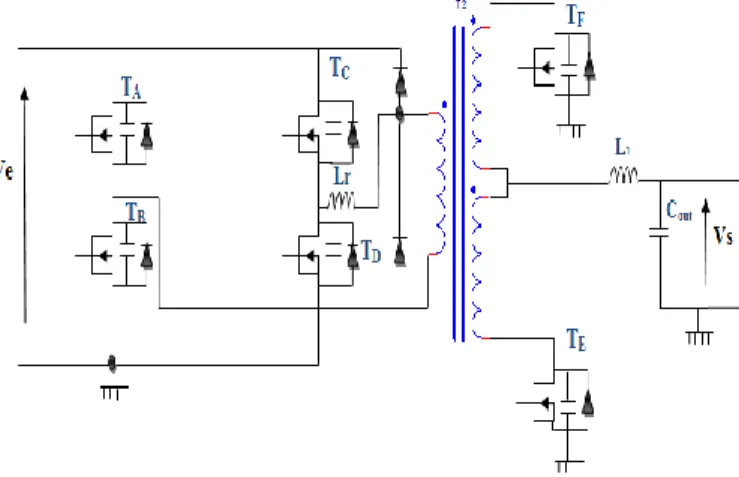
II. STRUCTURE AND OPERATION OF A FULL BRIDGE DC/DC CONVERTER CONTROLLED BY AN ANALOG CONTROL
Figure 1A represents the synoptic diagram of the Full Bridge DC/DC converter, with its analog control high controlled power an analog. Figure 1B, represents a full bridge DC/DC converter. With four transistors ( TA, TB, TC, and TD
)in the primary side of the transformer. TE, and TF represent the
transistors on the secondary side of the T2 transformer. While
LOut and VOut form the output filter. The Tr inductance is
designed to assist the T2 transformer leakage inductance when operating in resonance with the internal capacity of the MOSFET and facilitates zero voltage switching (ZVT). We have used silicon carbide-based transistors (C2M0025120D).
Figure1. DC/DC Full Bridge converter scheme
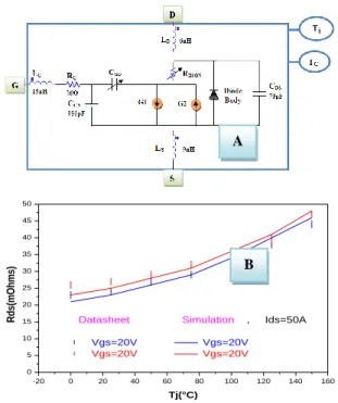
To monitor their operation, we conducted an electro-thermal study of this kind of transistor (Figure 2a) in order to evaluate the evolution of the junction temperature during its operation. Figure 2b shows the simulation results and with datasheet ones [12], the variation of the Drain-Source resistance (Rdson) as a function of temperature, for a current value of 50A.. It appears that the electro-thermal model developed during this work shows a good precision close to the optimum operating conditions given by the datasheets even in the case of very high temperatures (>150 °c), which confirms the high temperature operations of SIC transistors.
The design of an analog control with soft switching In order to design a simple analog control suitable for high power applications, we have studied and designed a simple analog control, it is based on the acquisition of the current image generated by the input generator and the output voltage we have also generated 6 PWM synchronized signals to ensure the switching of the 4 Transistors (TA, TB, TC, TD) on the primary side of the transformer and those on the secondary side (TE, TF) (Figure 1).
-20 0 20 40 60 80 100 120 140 160 0 5 10 15 20 25 30 35 40 45 50
Datasheet Simulation , Ids=50A
Vgs=20V Vgs=20V Vgs=20V Vgs=20V R d s( m O h m s) Tj(°C)
Figure 2: A: Electrical model of SiC (C2M0080120D). B: Rdson variation Vs junction temperature
The operating principle of this control is as follows:
❖ A proportional and integral PI : which regulates the output voltage in order to correspond to a given reference. As shown in Figure 3, using a particular bridge circuit The two voltages V1 and Vref are connected respectively to the non-inverting and inverting input of the proportional and integral amplifier PI.
❖ A progressive start circuit (Figure 3):.This circuit allows to generate a voltage that increases slowly until it reaches the maximum value. The purpose of adding this circuit to the PI controller is to generate a progressive cyclic ratio in transient mode.
❖ The Acquisition of the current was carried out on the basis of the circuit shown in Figure 4A, the transfomer used for this application has a transformation ratio (m) of 100 and the maximum voltage applied to the CS pin is Vp = 2V. ❖ From this data, we calculate the values of the resistances
(R1 and Rcs) in Figure 3A:
1 1
*
1
(
) *
6.88
*
2
* 2 *
INMIN MAX L p MAG SWV
D
I
Ps
I
A
Vs
m
L
F
=
+
+
=
1 ( 0.3) 20.89 ( *1.1) p CS p V R I n − = = (1)R
7
=
n R
*
CS
=
800
(2)❖ The signal that represents the current image at the input of the Full Bridge DC/DCconverter is added to a saw-tooth signal (VRAMP) (Figure 4B), using a summer Opampl circuit. Next, the resulting signal is compared with the VS1 signal generated by the circuit in Figure 3. And as a result, this comparison results in a PWM signal. The simulation results are shown in Figure 4.
V V U4 uA741 + 3 -2 V+ 7 V-4 OUT 6 OS1 1 OS2 5 Vs1 C21 560p IC = -1 R45 2.37k VBIAS3 D20 D1N5406 0 C23 5.6n IC = -1 R53 2.37k Vpi V1 0 Vref VBIAS2 R54 2.37k C24 1u IC = 5 R55 9.09k R56 27.9k Vout D21 D1N5406 D22 D1N5406 I1 25uAdc Vssc C22 10n VBIAS1 0 Figure.3. PI Corrector
The PWM signal obtained above is connected with a flip flop JK toggle (Figure 6). The Q output of this toggle will only change the state if the PWM signal connected to its CLK input is in the rising front. The signal Q and q ̅ at the output of the JK are two PWM signals (QC and QD) that will control an arm of the transistors of the DC/DC converter Full Bridge.
Then, we applied a delay of 360ns to the front amount of two signals Q and (q) ̅, which ensures a switching to zero voltage SVA (soft switching), avoiding the switching losses that usually occur during a Operation and a classical PWM delay.
0 CS Rcs D20DN4148 T 1 N = 100 R1 Vinput 410Vdc 0 DC/DC Converter
Figure.4 A : Input curent acquisition B
A A
V s1 V ra m p P WM U5A L M3 1 9 O UT 1 2 + 4 -5 G 3 V + 1 1 V -6 V BIA S2 R49 4 .7k 0 IN1 OUT IN2 R64 1 k Cs1 C29 3 30 p 0 Cs 0 V 40 T D = 0 T F = 5u P W = 0 u P ER = 5 u V 1 = 0 T R = 5u V 2 = 0.6 5 V s2
Figure.4 B: Input Current comparison with comparison Vs
Time
680us 685us 690us 695us 700us V(Startup.VS2) V(Startup.VS1) 0V 0.5V 1.0V 1.5V 2.0V Time
680us 685us 690us 695us 700us V(Startup.PWM)
0V 2.0V 4.0V 6.0V
Figure.5 Generated signals by Circuits of figures 2 &3
C: Signals comparison Vs of figure 2 and Vs1 of figure 3;
D: PWM signal at comparator output of figure 3B.
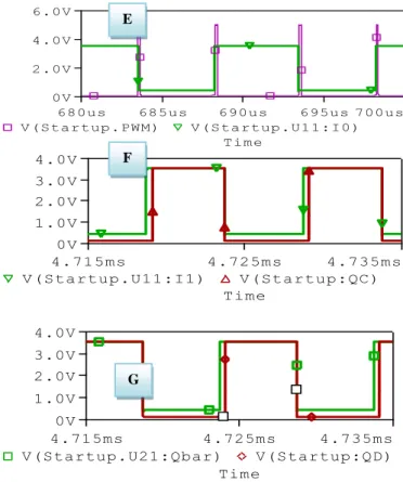
The simulation results are shown in Figure 7, by connecting the PWM signal obtained to a JK flip flop, we obtain the signal from Figure 6 in green. One notices the JK has a rising edgebehavior .for its state changes . The outputs Q and Q-, at the output of the JK flip flop, are shifted at each front up to 60ns.(7 F and G). U21 JKFF_ABM J CLK K Q Q PWM VBIAS U11 AND2 1 2 3 U12 AND2 1 2 3 QC QD U25 360ns DELAY U26 360ns DELAY
Figure.6 PWM signals connected to transistors TC et TD.
Time
680us 685us 690us 695us 700us V(Startup.PWM) V(Startup.U11:I0) 0V 2.0V 4.0V 6.0V Time 4.715ms 4.725ms 4.735ms V(Startup.U11:I1) V(Startup:QC) 0V 1.0V 2.0V 3.0V 4.0V Time 4.715ms 4.725ms 4.735ms V(Startup.U21:Qbar) V(Startup:QD) 0V 1.0V 2.0V 3.0V 4.0V
Figure 7. Signals generated by the circuit in Figure 5: E: PWM signal connected to the flip flop JK input (pink) and the one at its output (green); F: PWM signal QC (in red) of the JK flip flop (in green); G: QD PWM signal (in red).the output (Qbar) of the JK flip flop (in green).
Following the same principle, we generated the other two second-arm PWM signals from the Full Bridge DC/DC converter (Figure 8). Such as, by connecting a CLK signal of cyclic ratio of 0.05 to the CLK input of the Flip Flop JK, resulting in two output Q and (Qbar) . By imposing in the same way a delay of 360ns on the front amount of each output, we deduct the other two PWM signals (QA and QB) of the primary part. Figure 9 shows the simulation results of the signals generated by the circuit in Figure 8.
U27 A ND2 1 2 3 U28 A ND2 1 2 3 U29 3 60 n s DEL A Y U30 3 60 n s DEL A Y Q B Q A CLK V BIA S U17 JKFF_A B M J CLK K Q Q 0 V 42 T D = 0 T F = 25 n P W = 4 .5 u P ER = 5 u V 1 = 5 T R = 25 n V 2 = 0 CLK
Figure.8 PWM signals connected to transistors TA et TB C D E G B F
Time 4.715ms 4.725ms 4.735ms V(Startup.CLK) V(Startup.U27:I1) 0V 2.0V 4.0V 6.0V Time 4.715ms 4.725ms 4.735ms V(Startup.U27:I1) V(Startup:QA) 0V 1.0V 2.0V 3.0V 4.0V Time 4.715ms 4.725ms 4.735ms V(Startup.U17:Qbar) V(Startup:QB) 0V 1.0V 2.0V 3.0V 4.0V
Figure.9 H: Clock signal (in green)) connected to the flip flop JK input and
the one to its output (red);
I: QA (green) PWM signal at the output of the JK flip flop (in red)
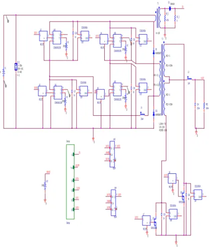
III. SIMULATION RESULTS AND INTERPRETATION Fig 10, represents the complete circuit of the switching mode power supply, implanted in the PSPICE simulator. We represent in the following the different simulation results obtained.
III.2
Performance comparison of the designed control and the UCC28950 controllerIn order to show the performance of the analog control designed during this work, we compared the different signals of the Full Bridge converter in Figure 1b, controlled by the designed control and the UCC28950 controller. The different results obtained are shown in Figure 11.Il is to note that the results of the system controlled by the analog control designed are shown in Figure 11 on the left and those of system controlled by UCC28950 [11] are shown on the Same figure on the right. Based on the results obtained:
0 0 0 C19 5n U37 C3D10065A A 1K 2 CASE3 C20 5n U38 C3D10065A A 1K 2 CASE3 L3 2uH L6 26uH I V V V V C15 5n C16 5n C17 5n C3_2 ESR = 0.01 X = 1 C = 330u IC = 400 C18 5n V1 410Vdc OUTC U39 C2M0080120D D 1 G 2 S 3 TJ4 TC 5 U40 C2M0080120D D 1 G 2 S 3 TJ4 TC5 U41 C2M0080120D D 1 G 2 S 3 TJ4 TC5 U42 C2M0080120D D 1 G 2 S 3 TJ4 TC5 R52 240m CS VOUT V2 25Vdc V3 25Vdc V4 25Vdc V5 25Vdc 0 0 R1_2 8 0 0 0 U6 IR2111 1 1 22 3 3 U7 IR2111 1 1 22 3 3 0 0 OUTF D1 DN4148 Q6 FDP032N08 Q5 FDP032N08 T1 N = 100 R2_2 4.87k C14 125m D11 MURS360T3 D5 MURS360T3 OUTE OUTB OUTA VOUTP CS Startup Startup Cs Vout QC QD QA QB OUTC OUTD U43 RSFF SE 1 CLK 2 RE 3 Q4 Q5 U44 RSFF SE 1 CLK 2 RE 3 Q4 Q5 VBIAS2 VBIAS2 OUTA OUTC OUTB OUTD OUTF OUTE V37 5Vdc VBIAS2 0 U22 C3D10065A A 1K 2 CASE 3 T2 LLEAK = 7.5u NP1 = 21 RP1 = 0.215 LM = 2.6m NS1 = 1 RCORE = 100K RS1 = 0.58m NS2 = 1 RS2 = 0.58m U2 IR2111 1 1 22 3 3 U3 IR2111 1 1 22 3 3 U4 IR2111 1 1 2 2 3 3 U5 IR2111 1 1 2 2 3 3 U23 C3D10065A A 1K 2 CASE3 OUTA OUTB OUTD U24 C3D10065A A 1K 2 CASE3 U25 C3D10065A A 1K 2 CASE3
Figure. 10 Complete circuit of the Supply switch mode
➢ The comparison of the OUTA PWM signal generated by the two controls shows that they have the same cyclic ratio of 0.47, the same frequency of 100kHz.
Time 5.00ms 5.01ms 5.02ms 5.03ms V(OUTA) V(OUTB) 0V 1.0V 2.0V 3.0V 4.0V
Time
5.00ms
5.01ms
5.02ms 5.03ms
V(OUTA)
V(OUTB)
0V
4V
8V
12V
16V
Figure 11. OUT A PWM signal,
H
I
➢ The currents (Figure 12A and B), which flow in the transistor TF of the second part, generated by the two commands are identical
Time 5.00ms 5.01ms 5.02ms 5.03ms I(T2:S1A) 0A 10A 20A 30A 40A 50A 60A Time 5.00ms 5.01ms 5.02ms 5.03ms I(T2:S1A) 0A 10A 20A 30A 40A 50A 60A
Figure .12 Output transformer current generated
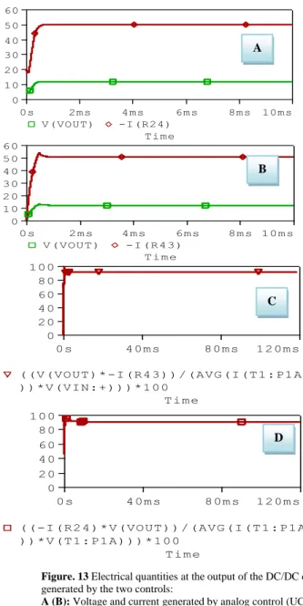
➢ The electrical quantities at the output (voltage, current) generated by the analog control designed (Figure 13 A) are identical with those generated by the UCC28950 (Figure 13 B). Then, the electrical quantities generated by the controls respond well to the defined load specification: a voltage, a currentand a power output of 12V, 50A and 600W respectively
➢ The analog control designed in this work has a satisfactory performance, it is higher than 90% (figure 13C). It is identical to that generated by the UCC28950 controller (figure 13D).
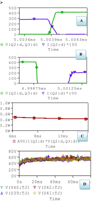
➢ The analog control designed during this work generates well-synchronised PWM signals, which ensures smooth switching to the transistors of the DC/DC converter. In order to clearly show these advantages, we have shown in Figure 12 and F, the power losses and the junction temperature of the four transistors, of the Full Bridge DC/DC converter (Figure 1), during the transistor switching. It appears that, the power losses in each transistor is low, they do not exceed 0.5W. Then the junction temperature of each transistor is about 50 °C. The results obtained clearly show the advantage of the control designed during this work
Time 0s 2ms 4ms 6ms 8ms 10ms V(VOUT) -I(R24) 0 10 20 30 40 50 60 Time 0s 2ms 4ms 6ms 8ms 10ms V(VOUT) -I(R43) 0 10 20 30 40 50 60 Time 0s 40ms 80ms 120ms ((V(VOUT)*-I(R43))/(AVG(I(T1:P1A ))*V(VIN:+)))*100 0 20 40 60 80 100 Time 0s 40ms 80ms 120ms ((-I(R24)*V(VOUT))/(AVG(I(T1:P1A ))*V(T1:P1A)))*100 0 20 40 60 80 100
Figure. 13 Electrical quantities at the output of the DC/DC converter
generated by the two controls:
A (B): Voltage and current generated by analog control (UCC28950)
C (D): Overall output of the converter controlled by the digital control (UCC28950).
III.2
Power losses study of the DC/DC converterThe analog control designed during this work generates well-synchronized PWM signals, which ensures soft switching of the transistors of the DC/DC converter. In order to clearly show these advantages, we have shown in Figure 14, the drain current C and the VDS voltage of the DC/DC converter. It should be noted that the current is multiplied by 100 in order to clearly notice the power losses during the transistor switching. It appears that: ➢ At the opening of the TA transistor (Figure 14 A), it is
noted that the VDS voltage toggles from 0 to 400V in few
nanoseconds time and the current ID changes from the max
to 0 gradually, leading to a very small power loss. While
B A D C A B
at the closing (Figure 14 B), the VDS voltage diverges
directly to 0. On the other hand, the current ID is delayed (1.5 µs) so that it toggles from 0 to its maximum value giving also a very small power loss(Figure 14 C) Then the junction temperature of each transistor is about 50 °C(figureD). The results obtained show clearly the advantage of the control designed during this work ➢ Time 5.0036ms 5.0039ms 5.0043ms V(Q2:d,Q3:d) I(Q2:d)*100 0 100 200 300 400 500 Time 4.99875ms 5.00125ms V(Q2:d,Q3:d) I(Q2:d)*100 0 100 200 300 400 500 Time 6ms 8ms 10ms 12ms AVG(I(Q2:d)*V(Q2:d,Q3:d)) 0W 0.2W 0.4W 0.6W 0.8W 1.0W Time 0s 20ms 40ms 60ms 80ms V(U40:TJ) V(U42:TJ) V(U39:TJ) V(U41:TJ) 0V 20V 40V 60V 80V
Figure 14 : Voltage VDS and current ID of the DC/DC converter TA in Figure 1: A and B: Voltage VDS and current ID at the opening and closing of the
transistor. C: Dissipated losses in the TA transistor. D: Temperature junction (1V=1°C)
IV. CONCLUSION
The development of a power supply with a relatively high current is presented. It allows to generate a voltage of 12v and a current of 50A, ( 600kW). It operates at a switching frequency of 100 kHz. The used structure is a Full Bridge DC/DC converter controlled by an analog control, developed and designed during this work. The challenge was to show that the analog control could advantageously be used instead of a digital one as the one commercialized by the Texas Instrument (UCC28950. The different results obtained show that the proposed control has relevant results similar to those obtained by the digital control.
References
[1] E. Baghaz, M. Melhaoui, M. F. Yaden and K. Kassmi. Photovoltaic System Equipped with a DC/DC Buck Converter and a MPPT
[2] http://vincent.boitier.free.fr/TER/809PET-boost-converter-efficiency-calculations.pdf
[3] Elhadi BAGHAZ. Architectures discrétisées de gestion de l’énergie fournie par les systèmes photovoltaïques. Thèse soutenue à l’université Mohamed Premier d’Oujda, Juin 2015.
[4] Cedric Cabal. Optimisation énergétique de l'étage d'adaptation électronique dédié à la conversion photovoltaïque. Thèse Délivrée par l’Université Toulouse III – Paul Sabatier, décembre 2008.
[5] L. Balogh, “The current-doubler rectifier: An alternative rectification technique for push-pull and bridge converters,” Unitrode Integrated Circuit Corporation, Design note, DN-63, 2001, pp.1–5.
[6] L. Balogh, “Design Review :100 W, 400 KHz DC-DC converter with current doubler synchronous rectification achieves 92% efficiency”. Texas Intrument, Design Review, 2001, pp.1–40.
[7] Z. Sun, B. Eng, “Full bridge DC/DC converter with zero current switching synchronous rectification for auxiliary power units, ”McMaster University, 2014.
[8] X. Zhao, J.M. Guerrero, and X. Wu ,’’Review of aircraft electric power systems and architectures,’’ in Proc. IEEE International Energy Conference (EnergyCon’14), 2014.
[9] N. Kutkut, “A full bridge soft switched telecom power supply with a current doubler rectifier,” in Proc. Telecommunications Energy Conference, 1997. INTELEC 97., 19th International, Melbourne, Vic., 19–23 Oct 1997, pp.344–351
[10] M. O’Loughlin, “UCC28950 600-W, phase-shifted, full-bridge application report,” TI Lit. No. SLUA560B, pp. 1–30, Sept. 2010. [11] http://www.ti.com/lit/ds/symlink/ucc28950.pdf [12] http://www.wolfspeed.com/media/downloads/161/C2M0025120D.pdf A B C D