RESEARCH OUTPUTS / RÉSULTATS DE RECHERCHE
Author(s) - Auteur(s) :
Publication date - Date de publication :
Permanent link - Permalien :
Rights / License - Licence de droit d’auteur :
Bibliothèque Universitaire Moretus Plantin
Institutional Repository - Research Portal
Dépôt Institutionnel - Portail de la Recherche
researchportal.unamur.be
University of Namur
Experimental evidence of surface-plasmon coupling in anisotropic hollow
nanoparticles
Kociak, M.; Stéphan, O.; Henrard, L.; Charbois, V.; Rothschild, A.; Tenne, R.; Colliex, C.
Published in:
Physical review letters
Publication date: 2001
Link to publication
Citation for pulished version (HARVARD):
Kociak, M, Stéphan, O, Henrard, L, Charbois, V, Rothschild, A, Tenne, R & Colliex, C 2001, 'Experimental evidence of surface-plasmon coupling in anisotropic hollow nanoparticles', Physical review letters, vol. 87, no. 7, 075501, pp. 075501/1-075501/4.
General rights
Copyright and moral rights for the publications made accessible in the public portal are retained by the authors and/or other copyright owners and it is a condition of accessing publications that users recognise and abide by the legal requirements associated with these rights. • Users may download and print one copy of any publication from the public portal for the purpose of private study or research. • You may not further distribute the material or use it for any profit-making activity or commercial gain
• You may freely distribute the URL identifying the publication in the public portal ?
Take down policy
If you believe that this document breaches copyright please contact us providing details, and we will remove access to the work immediately and investigate your claim.
Experimental Evidence of Surface-Plasmon Coupling in Anisotropic Hollow Nanoparticles
M. Kociak,1O. Stéphan,1L. Henrard,2 V. Charbois,1A. Rothschild,3R. Tenne,3and C. Colliex1,4
1Laboratoire de Physique des Solides, Associé au CNRS, Bâtiment 510, Université Paris-Sud, 91405, Orsay, France 2Laboratoire de Physique du Solide, Facultés Universitaires Notre-Dame de la Paix, 61 rue de Bruxelles, 5000 Namur, Belgium
3Weizmann Institute, Rehovot 76100, Israel
4Laboratoire Aimé Cotton, Bâtiment 505, Université Paris-Sud, 91405 Orsay-Cedex, France
(Received 2 March 2001; published 26 July 2001)
We report on the investigation of surface-plasmon excitation of anisotropic WS2hollow nanoparticles
in a near-field geometry by means of a scanning transmission electron microscope. The shell thickness influence on the electron-energy-loss-spectroscopy spectra is experimentally observed and is analyzed within a classical dielectric formalism. As for the isotropic case, we evidence one symmetric (tangential) and one antisymmetric (radial) mode. We point out the intriguing fact that, for the anisotropic case, one can relate these modes to the interband transition of the in-plane component of the dielectric tensor and to the bulk-plasmon energy of the out-of-plane component.
DOI: 10.1103/PhysRevLett.87.075501 PACS numbers: 61.46. +w, 68.37.Ef, 78.67.Ch
As the size of artificial or natural nanostructures de-creases, it is important to understand their intrinsic prop-erties compared to bulk ones. It is particularly the case for their optical and dielectric properties, i.e., the response of the valence electrons of the nanostructure to a given applied electromagnetic field. This has been clearly emphasized in recent experiments involving photon beams, both in far-field [1] and near-far-field [2 –4] geometries, as well as in elec-tron spectroscopy on thin films [5] and nanospheres [6].
The electromagnetic response of such nanoparticles is described by their polarizability, which is defined as the proportionality coefficient connecting the external applied potential to the induced one. The surface-plasmon excita-tions that are the main concern of this Letter are described in terms of resonances in the polarizability. Hereafter, we deal with the classical dielectric model for which the polar-izability is obtained from the bulk dielectric tensor e共v兲. For isotropic materials, the common interpretation scheme of the v dependence of the bulk dielectric function e共v兲 is that the maxima of the imaginary part e2are associated with interband transitions (IT) and describe macroscopi-cally the resonant absorption of photons by the medium. The zeros of the real part e1 (combined with a vanishing e2) are called volume plasmon excitation and correspond to the polarization eigenmodes of the infinite medium. For anisotropic materials, the previous considerations re-main valid but imply various combinations of the tensor component.
In finite systems, where boundaries play a large role, surface and interface excitations add their contributions to the bulk excitations. These resonances (modes) are red-shifted compared to bulk-energy modes and directly reflect the geometry of the object: for example, translationally (rotationally) invariant objects have modes indexed by a kinetic (angular) momentum. For isotropic media, this can be illustrated within a simple Drude model for which sur-face modes arise at vpp
2 in the case of a half-space or at q
l
2l11vp for a filled sphere (l is the angular momentum
and vp is the plasma frequency of the bulk material). For
an object of finite thickness, a slab (or a hollow sphere) for example, such modes split into two branches, one sym-metric (tangential) and one antisymsym-metric (radial), which merge for high thickness of the object or, equivalently, for large momentum transfer [7,8]. The existence of these symmetric and antisymmetric branches was demonstrated experimentally in thin Al foils [5] by electron-energy-loss spectroscopy (EELS) in transmission. The influence of the geometry on the surface-plasmon energy of nanospheres has been shown by spatially resolved EELS in a scanning transmission electron microscope (STEM) [6,9].
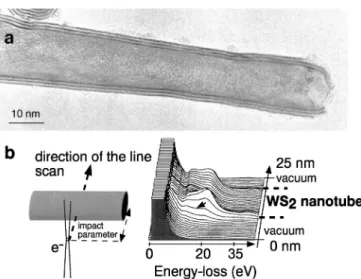
In a hollow nanostructure, such as nanotubes or hyper-fullerenes, the role of surface is even more pronounced and the understanding of the surface effect on the electro-magnetic response of the nanoparticle becomes essential. Moreover, the anisotropy of the nanostructure, which can be local (i.e., the principal crystallographic axis changes rapidly on the scale of the nanostructure), can also greatly affect this surface coupling phenomenon and then the di-electric response of a nanostructure [10– 15]. As a mat-ter of fact, when anisotropy is concerned, the connection between the anisotropy, the symmetry, and the energy of the excitations has to be reconsidered. In this Letter, we address these questions by means of an investigation that combines experimental and theoretical approaches to the surface coupling effect in a cylindrical anisotropic mate-rial (WS2nanotube) in a near-field geometry. WS2 nano-structures were selected to perform this study because they offer the best versatility in terms of accessible inner and outer diameters, and allow us to distinguish anisotropy and surface coupling effects. WS2nanotubes were synthesized according to the procedure described in [16]. Typically, a synthesis yields a large variety of tube diameters, from the thinnest constituted by two or three walls (see a TEM image of a three-wall nanotube in Fig. 1a) to the thickest 075501-1 0031-9007兾01兾87(7)兾075501(4)$15.00 © 2001 The American Physical Society 075501-1
FIG. 1. (a) High-resolution image of a three-wall WS2
nano-tube. (b) A series of spectra acquired while scanning the STEM probe, with corresponding geometry. The arrow indicates the surface of the tube, which can be accurately determined.
having 20 walls. WS2nanotubes are made up of rolled-up
WS2hexagonal sheets interacting weakly via van der Waals forces. Each sheet is a sandwich of three layers (S-W-S) with covalent tetrahedral W-S bonds. Such structure is lo-cally preserved in the nanotubes, which then are lolo-cally anisotropic. The anisotropic axis (c axis) is defined as the axis locally perpendicular to the sheets. In the following, parallel (perpendicular) means parallel (perpendicular) to this axis.
EELS in a STEM is an appropriate tool to investigate such polarizability properties [17– 19]. Moreover, its analysis ability at a nanometer scale makes it a per-fectly suited technique for the investigation of individual nanoparticles for which strong surface effects are expected. In order to record low-loss EELS spectra (1– 50 eV), we have used a STEM in a near-field geometry, where a 0.5-nm probe is positioned at grazing incidence (about 0.5 nm) of a tube (see inset of Fig. 2). The probe position can be monitored with an accuracy better than 0.25 nm. Figure 1b shows a collection of spectra acquired every 3 nm along a line scan across a nanotube of the same di-mensions as the one in Fig. 1a. The spectrum acquired at grazing incidence is shown by an arrow. In such geometry only surface modes are excited. The spectra were acquired using a Gatan 666 parallel EELS spectrometer, providing a 0.5-eV resolution with an acquisition time of 0.4 s.
In our previous studies [10] on carbon and boron nitride (BN) nanotubes and nanospheres the coupling effects were not investigated because only thick hollow nanoparticles were fully analyzed. Here, we will show that (1) as for the isotropic and ideal case (i.e., where bulk and thus surface modes are well defined), the surface coupling is revealed by the occurrence of two distinct intensity bands in the EELS spectrum for small wall thickness, with either pure symmetric or antisymmetric character. These bands merge (for thicker wall objects) into a single band. (2)
More-FIG. 2. Experimental (upper curves) and simulated (lower curves) loss spectra for thin (left side) and large (right side) WS2 nanotubes. Geometry of the experiment and of the tubes
are schematically described in the insets.
over, for small shell thickness, the excitation modes of the anisotropic nanoparticles present the following peculari-ties: low-energy (symmetric) excitation modes occur at the position of the IT associated with the in-plane component of the dielectric tensor, while the high-energy (antisymmet-ric) excitation modes occur at the position of the bulk plas-mon energy associated with the out-of-plane component.
Experimental data for two extreme situations are shown in Fig. 2. The EELS spectrum from the thinnest tube (Fig. 2a), with external and internal radii R 苷 7.4 nm and r 苷 6.0 nm, respectively, presents a forest of peaks from 0 to 15 eV, and an isolated peak at 22 eV, while that of the thicker nanotube [(see Fig. 2b) R 苷 20.5 nm,
r 苷 10.5 nm] shows a broad maximum centered about
16 eV and weaker oscillations at lower energy. Although they mostly differ by the wall thicknesses of the particles, these spectra are strikingly different, and such large varia-tions do not seem to have ever been observed for any type of nanoparticles or thin films.
For the sake of interpreting the data, we have performed EELS simulations by using the dielectric model in the elec-trostatic limit [7,12,14,20], which proved to be reliable for both isotropic [6] and anisotropic [10] nanoparticles. Briefly, an electron traveling aloof a particle along a clas-sical trajectory excites its surface dielectric modes, which gives rise to an induced field acting back on the electron, producing an energy loss. In [10], we have shown that the main features of the EELS spectra of carbon and BN cylin-ders can satisfactorily be accounted for, using a simulation for a sphere. As this last geometry is more convenient to deal with, we have therefore performed EELS simulations for WS2spheres. The dielectric tensor for bulk planar WS2 was used for all additional simulations of polarizabilities. It was computed in the optical limit with ab initio cal-culated wave functions using the density functional theory within the local density approximation. Our choice of such a dielectric tensor relies on a satisfactory agreement with experimental values of e共v兲, when available, i.e., for the e⬜ case.
The EELS spectrum for a sphere is given by [20]
P共v, b兲 苷 SlCl共v, b兲 Im关al共v兲兴, where l is the angular
momentum transfer, Cl is the kinematic factor, b is the
impact parameter (i.e., distance from the beam to the cen-ter of the particle), and al is the response of the particle
to a multipolar field of order l. Cl depends on the
experimental conditions (impact parameter, acceleration voltage). The polarizability al depends uniquely upon
the aspect ratio of the particle (inner and outer radii), and on the dielectric tensor of the bulk material [12,14]. Applied to our case, both thin and thick anisotropic shell simulated spectra are shown in Fig. 2, and fit surprisingly well with experimental data despite the lack of similarities between the two cases. This shows that the dissimilarities observed for a specimen of the same nature but different thickness are not due to microscopic phenomena and can be interpreted within the dielectric formalism.
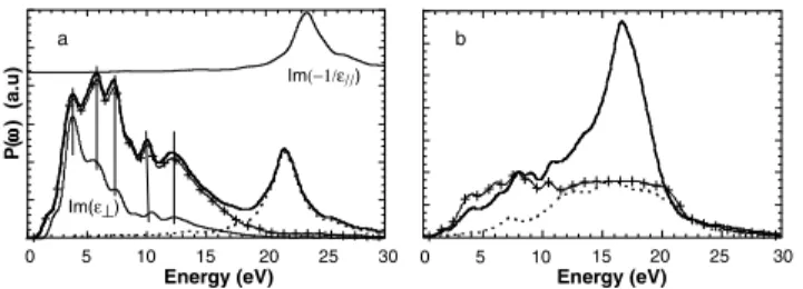
In order to attribute different features of the spectra to specific excitations, we computed the spectra for both the thin and thick tubes, while setting successively either ek or e⬜ equal to unity. In such a description, the material cannot be polarized along one (parallel or perpendicular) crystallographic axis. In Fig. 3a, we show that the spec-trum of the thin shell tube is the sum of the two contribu-tions. Then, one can directly attribute the high-energy peak to excitations related to ek, and the low-energy features to those of e⬜. On the other hand, such a decomposition fails to describe the thick tube features, as proven by Fig. 3b.
The thickness of the particle seems to be the parameter of importance, much more than the geometry — spherical, cylindrical, or planar. Consequently, we propose to further develop our interpretation by using a simple anisotropic
0 5 10 15 20 25 30 Energy (eV) 30 P( ωωωω ) (a.u) 0 5 10 15 20 25 Im(ε⊥) Im(−1/ε//) Energy (eV) a b
FIG. 3. Calculated spectra for small (a) and thick (b) nano-tubes using a dielectric model for spherical particles. Solid lines: calculated spectra using ab initio dielectric constant. Dashed lines: same calculations, with e⬜苷 1. Cross dots: same
calcu-lations with ek苷 1. Im共e⬜兲 and Im共21兾ek兲 are also shown in
the left panel.
slab model, which can be analytically worked out much more easily than a curved shell model. Let us assume that we are studying a WS2 slab of thickness d, with an elec-tron traveling parallel to the slab at an impact parameter
b, a situation which will prove to account for the main physics of our experiment. In this case, the c axis of the material is perpendicular to the slab surface. This situation remains locally valid in spherical and cylindrical geometry. The geometrical out-of-plane (in-plane) direction is then equivalent to the anisotropic parallel (perpendicular) direc-tion. The EELS spectrum can then be computed as [21]
P共v, b兲 苷Z
`
0
dk CK共v, b兲 Im关gK共v兲兴 ,
where K 苷pk21 v2兾y2 is the modulus of the trans-ferred momentum, k is its component within the plane of the surface, and the response function [the formal equiva-lent of al共v兲 for the planar case] reads [13]
gK共v兲 苷 2 关1 2 ek共v兲e⬜共v兲兴sh共Kdpl兲 关1 1pek共v兲e⬜共v兲 兴2eKd兾 p l2 关1 2pe k共v兲e⬜共v兲 兴2e2Kd兾 p l, where l 苷 ek共v兲 e⬜共v兲 and CK共v兲 ~ e 2Kb is the kinematic factor.
A direct comparison between the slab parameter, Kd, and the sphere parameters l, r, R can be made by means of the relation 关共1 2 Rr兲l 苷 Kd兴 [22]. Knowing that ex-perimentally l # 5 [10], we derive Kd # 0.5 for thin tubes (r兾R 艐 0.9) and 0.5 , Kd , 2.5 for thick ones (r兾R 艐 0.5). Let us comment on the two situations:
Kd ø 1 (thin tubes) and Kd ¿ 1 (thick tubes).
For Kd ¿ 1, the limit of gK共v兲 gives
gK共v兲 苷 2
1 2pek共v兲e⬜共v兲 1 1pek共v兲e⬜共v兲
which depends only on the geometrical average of the di-electric component, as was already shown for anisotropic half-space [13,23]. For an isotropic material (e⬜ 苷 ek 苷 e), one retrieves the standard surface dielectric response gK共v兲 苷 2
12e
11e [18]. If the resonances of the parallel and perpendicular dielectric components overlap in energy, as is the case for WS2, there is no possibility to discriminate between excitations related to an in-plane or out-of-plane
component of the dielectric tensor. This explains why the decomposition of the spectrum for a thick tube in Fig. 3b does not work.
In the limit Kd ø 1, we find gK共v兲 苷 Kd4 关e21k共v兲 1
e⬜共v兲兴, which is clearly disymmetric with respect to the ⬜ and k components. Resonances of Im关gK共v兲兴, and then
of P共v兲, occur at maxima of Im关e⬜共v兲兴 and Im关2e1k共v兲兴. In Fig. 3a we compare the calculation of the two terms of the analytical expression in the small Kd limit to the full simulation for a WS2 nanosphere. Considering that (i) the above expression has been obtained for an anisotropic slab and (ii) the small Kd limit is not fully reached, we clearly evidence two bunches of modes, as-sociated with resonances of Im关e⬜共v兲兴 and Im关2e1
k共v兲兴,
which merge in the case of thick tubes.
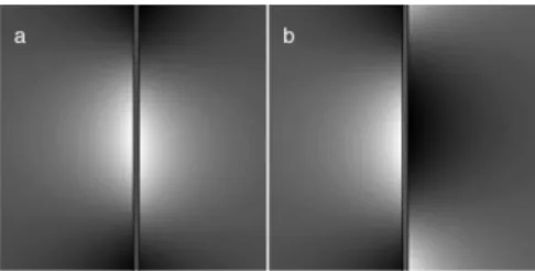
For ideal isotropic thin films, the surface coupling is re-sponsible for two branches of modes which are associated with the symmetric and antisymmetric behavior of the electric potential. As emphasized by the induced potential maps of Fig. 4, this association can be generalized to a real
FIG. 4. (a),(b) Maps of the induced potential of a WS2slab for
energies 7.8 and 23 eV. The maps are computed using an ab ini-tio dielectric constant and the electrostatic dielectric model, with no other fitting or approximation. Note the symmetric (antisym-metric) behavior of the low-energy (high-energy) excitation.
and anisotropic thin material. Indeed, the induced potential associated with any of the low energy modes [for instance, 7.8 eV (Fig. 4a)] and the one associated with the high-energy modes [for example, 23 eV Fig. 4b)] display, respectively, symmetric and antisymmetric behavior. Moreover, the link between the anisotropy and the sym-metry is clearly revealed, since we can associate the symmetric mode to a maximum of Im关2e1k共v兲兴 (Fig. 4a) and the antisymmetric mode to a maximum of Im关e⬜共v兲兴 (Fig. 4b). Further calculations show that a complete anal-ogy to the case of a slab can be made for an anisotropic shell: the tangential mode and the radial modes (as defined in the isotropic case [8]) are the counterparts of the symmetric and antisymmetric modes. This description is very similar to that for phonon excitation modes, where, for small thickness, modes decouple into longitudinal and transverse optical phonons [24].
In conclusion, the puzzle of the effect of surface cou-pling in anisotropic media has been solved by studying the surface modes of WS2 nanostructures with different geometries, using spatially resolved EELS. Beyond the isotropic case, we have shown that the surface coupling in an anisotropic nano-object results in the existence of sym-metric (tangential) and antisymsym-metric (radial) modes, even in real solids. Moreover, we reconsidered the definition of surface-plasmon resonances, as they arise at the
bulk-plasmon resonance of the parallel dielectric constant, and
at the interband transition of the perpendicular component of the dielectric tensor. The classical model is quite suc-cessful in interpreting our data even when the layers are a few atoms thick, similar to the case encountered when de-scribing optical properties of small clusters with dielectric theories [25].
We acknowledge E. Sandré for providing us with the
ab initio calculations, and Ph. Lambin and A. A. Lucas for
fruitful discussions. L. H. was supported by the Belgian National Fund (FNRS). This work was partly funded by
the Belgian Interuniversity Research Project on Reduced Dimensionality Systems (PAI-UAP P4-10).
[1] T. W. Ebbesen, H. J. Lezec, H. F. Ghaemi, T. Thio, and P. A. Wolff, Nature (London) 391,667 (1998).
[2] T. Klar, M. Perner, S. Grosse, G. von Plessen, W. Spirkl, and J. Feldmann, Phys. Rev. Lett. 80,4249 (1998). [3] N. Nilius, N. Ernst, and H. J. Freund, Phys. Rev. Lett. 84,
3994 (2000).
[4] J. R. Krenn, A. Dereux, J. C. Weeber, E. Bourillot, Y. Lacroute, J. P. Goudonnet, G. Schider, W. Gotschy, A. Leitner, F. R. Aussenegg, and C. Girard, Phys. Rev. Lett. 82, 2590 (1999).
[5] R. B. Pettit, J. Silcox, and R. Vincent, Phys. Rev. B 11,
3116 (1975).
[6] D. Ugarte, C. Colliex, and P. Trebbia, Phys. Rev. B 46,
1794 (1992).
[7] H. Raether, Surface Plasmon, Springer Tracts in Modern Physics Vol. 3(Springer-Verlag, Berlin, 1988).
[8] Ph. Lambin, A. A. Lucas, and J. P. Vigneron, Phys. Rev. B
46,1794 (1992).
[9] M. Achéche, C. Colliex, H. Kohl, A. Nourtier, and P. Treb-bia, Ultramicroscopy 20,99 (1986).
[10] M. Kociak, L. Henrard, O. Stéphan, K. Suenaga, and C. Colliex, Phys. Rev. B 61,13 936 (2000).
[11] T. Stöckli, J. M. Bonard, A. Châtelain, Z. L. Wang, and P. Stadelmann, Phys. Rev. B 61,5751 (2000).
[12] A. A. Lucas, L. Henrard, and Ph. Lambin, Phys. Rev. B 49,
2888 (1994).
[13] Ph. Lambin, P. Senet, A. Castiaux, and L. Philippe, J. Phys. I (France) 3,1417 (1993).
[14] L. Henrard and Ph. Lambin, J. Phys. B 29,5127 (1996). [15] C. Yannouleas, E. N. Bogachek, and U. Landman, Phys.
Rev. B 50,7977 (1994).
[16] R. Tenne, L. Margulis, M. Genut, and G. Hodes, Nature (London) 360,444 (1992).
[17] R. H. Ritchie, Phys. Rev. 106,874 (1956). [18] Z. L. Wang, Micron 27,265 (1996).
[19] H. Cohen et al., Phys. Rev. Lett. 80,782 (1998).
[20] T. L. Ferrell and P. M. Echenique, Phys. Rev. Lett. 55,1526 (1985); P. M. Echenique, A. Howie, and D. J. Weathley, Philos. Mag. B 56,335 (1987).
[21] P. E. Batson, Ultramicroscopy 11, 299 (1983); A. Howie and R. H. Milne, Ultramicroscopy 18,427 (1985). [22] L. Henrard, O. Stéphan, and C. Colliex, Synth. Met. 103,
2502 (1999).
[23] A. A. Lucas and J. P. Vigneron, Solid State Commun. 49,
327 (1984).
[24] K. L. Kliewer and R. Fuchs, Adv. Chem. Phys. XXVII,
355 (1974).
[25] C. Bréchignac, Ph. Cahuzac, and N. Kéba˝ıli, J. Leygnier, and H. Yoshida, Phys. Rev. B 61,7280 (2000).