Discovery of robust in-plane ferroelectricity in atomic-thick SnTe
The MIT Faculty has made this article openly available. Please sharehow this access benefits you. Your story matters.
Citation Chang, Kai et al. “Discovery of Robust in-Plane Ferroelectricity in Atomic-Thick SnTe.” Science 353, 6296 (July 2016): 274–278 © 2016 American Association for the Advancement of Science
As Published http://dx.doi.org/10.1126/SCIENCE.AAD8609
Publisher American Association for the Advancement of Science (AAAS)
Version Author's final manuscript
Citable link http://hdl.handle.net/1721.1/117744
Terms of Use Creative Commons Attribution-Noncommercial-Share Alike
Discovery of robust in-plane ferroelectricity in
atomic-thick SnTe
Kai Chang,
1,2∗Junwei Liu,
1,2,3∗Haicheng Lin,
1,2Na Wang,
1,2Kun Zhao,
1,2Anmin Zhang,
4Feng Jin,
4Yong Zhong,
1,2Xiaopeng Hu,
1,2Wenhui Duan,
1,2Qingming Zhang,
4,5Liang Fu,
3Qi-Kun Xue,
1,2Xi Chen,
1,2†Shuai-Hua Ji,
1,2,6‡1State Key Laboratory of Low-Dimensional Quantum Physics,
Department of Physics, Tsinghua University, Beijing 100084, China
2Collaborative Innovation Center of Quantum Matter, Beijing 100084, China 3
Department of Physics, Massachusetts Institute of Technology, Massachusetts 02139, USA
4
Department of Physics, Beijing Key Laboratory of Opto-electronic Functional Materials &Micro-nano Devices,Renmin University of China, Beijing 100872, China
5
Collaborative Innovation Center of Advanced Microstructures, Shanghai 200240, China
6
RIKEN Center for Emergent Matter Science (CEMS) - Wako, Saitama 351-0198, Japan
∗These authors contributed equally to this work
†Corresponding author. E-mail: xc@mail.tsinghua.edu.cn(X.C.) ‡Corresponding author. E-mail: shji@mail.tsinghua.edu.cn(S.-H. J.)
November 13, 2015
Stable ferroelectricity with high transition temperature in nano-structures are
long desired for miniaturizing future ferroelectric devices. The ultra-thin film
with nano-meter thickness is one of the promising directions. Here, we report
the discovery of the stable in-plane spontaneous polarization in atomic-thick
SnTe, down to 1 unit cell (UC) limit. The ferroelectric transition temperature
SnTe is only 98 K ). Moreover, 2-4 UC SnTe films show robust ferroelectricity
at room temperature. The interplay between semiconducting properties and
ferroelectricity in this two-dimensional material may enable a wide range
ap-plications in non-volatile high density memories, nano sensors and electronics.
Two-dimensional (2D) materials exhibit a wide range of symmetry breaking quantum phe-nomena such as crystalline order (1, 2), superconductivity (3, 4), magnetism (5, 6) and charge-density wave (7, 8), which persist in the limit of a single-unit-cell thickness. Compared with the aforementioned orders, ferroelectric order with long range dipolar interaction is more strongly coupled to the change of composition, surface charge and strain induced by external effect. It makes the studies on the ultra-thin ferroelectric film more complicated and difficult.
Intensive efforts have been made to explore the ferroelectricity in the ultra-thin film, even near the atomic limit thickness. For the perovskite ferroelectric materials, stable out-plane spontaneous polarization has been discovered in the thin films of few unit cells (UCs) thick-ness (9–12). Theoretical studies point out that the charge screening, chemical bonding and mis-fit strain at the interface may play a role in stabilizing ferroelectric states (13–18). The transition temperature in those ultra-thin films usually decreases as the thickness is reduced (10–12, 19), which could be understood by the depolarization field effect. In contrast, the transition temper-ature of ferroelectric polymer film is nearly thickness independent indicating two dimensional behavior (20).
Both synthesis and characterization of such ultra-thin ferroelectric sheets with atomic scale precise control pose great challenges. In this work, by using the state-of-art molecular beam epi-taxial technique, we prepare atomic thick ferroelectric SnTe films and discover stable in-plane spontaneous polarization in SnTe film of only one UC thickness, 0.63 nm. In order to avoid external strain effect, we employ the graphitized 6H-SiC(0001) substrate in epitaxial growth to obtain stress-free thin films. The substrate surface is mainly covered by the monolayer/bilayer
graphene. The weak Van der Waals bonding between substrate and SnTe film largely reduces the strain effect and helps to preserve the in-plane component.
In the bulk form, SnTe is a narrow-gap (∼ 0.2 eV) semiconductor (21) and possesses the rock salt structure with a lattice constant of 6.32 ˚A (Fig. 1A) at room temperature. SnTe is al-ways heavilyp-type doped because of the negative formation energy of Sn vacancy (22). At the ferroelectric transition temperatureTc, the crystal goes through a cubic-to-rhombohedral
struc-tural phase transition and the two sub-lattices of Sn and Te atoms are displaced from each other along the [111] direction, forming the ferroelectric state (23, 24). Due to the screening effect of charge carriers, Tc drops rapidly as the concentration of Sn vacancy increases (25) and the
highest transition temperature of bulk SnTe is only 98 K (26). Recently, interests in the ferro-electric structural distortion in SnTe are rekindled by its strong impact on electronic properties of the topological crystalline insulator phase newly discovered in IV-VI semiconductors (27).
The SnTe films grown on SiC are characterized by the in situ reflective high energy elec-tron diffraction (RHEED) (Fig. S1(a)) and scanning tunneling microscopy (STM) topography images (Figs. 1B, S1(b)). At low coverage, the (001)-orientated islands are formed on the sub-strate. In contrast to the case involving strong directional covalent bonds, the lattice matching conditions are largely relaxed in the Van der Waals epitaxy. As a consequence, the in-plane orientation of the SnTe islands is randomly distributed. The weak bonding is also demonstrated by the fact that an entire island in size of 100 nm can be displaced by the STM tip (Fig. S2). By carefully controlling the substrate temperature and SnTe flux, the size of an island can be as large as ∼ 1 µm (Fig. S13). The facet edges along the [100] and [010] directions are clearly seen in the STM images. The island thickness corresponds to an integer multiple of the SnTe unit-cell (no half layer), being consistent with the formation energy calculation (Fig. S4). The topography images (Fig. S5(a)) also indicate that the formation of Sn vacancies is greatly sup-pressed in the atomic-thin SnTe films. The surface defect density is1010
∼1011
UC film and even lower for the 1 UC one. Both are much lower than that of the bulk material (∼ 1013
cm−2). The electronic density of states of 1 UC SnTe film is measured by scanning
tunneling spectroscopy (STS). The arrows in the dI/dV curve (Fig. 1C) indicate the band edges. The energy gap of 1 UC film rises to 1.5 eV from its bulk value 0.2 eV.
It is challenging to probe the ferroelectric properties of an ultrathin film because of the sig-nificantly reduced signal magnitude comparing with the bulk. Usually, more sensitive probes, such as the synchrotron X-ray scattering (10), ultraviolet Raman spectroscopy (12), the po-larized second harmonic generation measurement (28) and the piezoresponse force micro-scope (29), are employed to detect such weak signal. Furthermore, the small island size re-quires even more sensitive measurement with high spatial resolution. For the present study, we use STM and STS to probe the ferroelectricity of SnTe in the two dimensional limit. The ob-served evidences for ferroelectricity include the formation of domain structure (Fig. 1D), lattice distortion (Figs. 1E, 1F), band bending (Figs. 2A-D) and polarization manipulation by electric field (Fig. 2E).
The domain structure in 1 UC SnTe film is resolved in the STM image (Fig. 1D) at certain sample bias voltage (for example, −0.2 V). The parallel stripes are along the [010] direction. The atomically resolved image (Fig. 1D, left inset) shows a quasi-square lattice of Te atoms (the negative bias corresponds to the filled states mainly contributed by Te). The lattice constant ∼4.5 ˚A is in good agreement with the Te-Te distance in the (001) plane of bulk SnTe. The lattice is continuous across the domain boundary (Fig. 1D, left inset). Nevertheless, the Fourier transform of an area containing two domains (STM image in the inset of Fig. 1E) clearly exhibits two sets of Bragg peaks split along the [100] direction (Fig. 1E). Each set of the Bragg peaks is contributed by one domain (see the right panels of Fig. 1E). The lattice is slightly distorted from a perfect square to a parallelogram (Fig. 1F). From the Fourier transform, the two basis of the Te sub-lattice at liquid helium temperature are found to be 4.58 ± 0.05 ˚A and
4.44 ± 0.05 ˚A, respectively. The parallelogram is elongated along the [110] and its equivalent orientations (indicated by arrows in Figs. 1D-F). The elongated diagonals for two adjacent domains are perpendicular to each other. As shown later, the in-plane polarization is along those diagonals.
The domain formation and lattice distortion are still not adequate to serve as the conclusive evidence for ferroelectricity. A more direct manifestation comes from the band bending at the edge of an island. In general, the discontinuity of polarization on the border of a dielectric induces the polarization charge, whose density is given by P · n. Here P and n are the po-larization and the normal direction, respectively. So if one surface is positively charged, the opposite surface must be negatively charged. The electric field generated by the polarization charge shifts the bulk electronic bands (Fig. 2A). If there are free carriers owing to doping, the screening effect confines the band bending within the vicinity of the borders (Fig. 2A). Band bending has various origins and is commonly observed on surfaces. However, the unique fea-ture on the surfaces of a ferroelectric is that the bending directions are opposite to each other on the opposite surfaces of a domain; one side is upward and the other side is downward (30).
As a matter of fact, the signature of band bending has already emerged in Fig. 1D. In the STM image (constant current mode at −0.2 V), the height of the island edge is different from that of the bulk and the edges for two adjacent domains show opposite variation in height. The observed pattern can be easily explained by the band bending effect if the polarization direction is indeed given by the arrows in Fig. 1D. As illustrated in Fig. 2B, the band gap at an edge is shifted by the polarization charge. The positive charge moves the band downward and there is less density of states between the bias voltage Vs and the Fermi level. Therefore the apparent
height of a positively charged edge is lower than that of the bulk. Similarly, a negatively charged edge appears higher.
curve as a function of the distance to an edge (Fig. 2C). Spatially resolved dI/dV spectra are taken along the lines perpendicular to the edges of two adjacent domains. The peaks shift to opposite directions up to 0.2 eV with a screening length of about 10 nm. For comparison, the dI/dV mapping is also performed on a 1 UC PbTe island and shows no band bending effect (Fig. S13). PbTe is paraelectric, otherwise very similar to SnTe.
The above observations do not uniquely determine the orientation of polarization. Any configuration of polarization gives rise to similar band bending pattern if the projections of polarization on the normal direction of edge are opposite to each other between two adjacent domains in Fig. 1D. The polarization orientation is unequivocally determined by the band bending pattern on a single domain island (Fig. 2D). The reversed bending on the opposite edges of the squared island clearly demonstrates that the polarization of 1 UC SnTe film has in-plane component along the [110] diagonal.
With the in-plane polarization determined by lattice distortion together with the sign change of polarization charge on edges, we are able to classify the different types of domain walls. The straight domain walls in Fig. 1D belong to the 90◦ “head-to-tail” type. The “head-to-head” domain wall in Fig. 2E shows the zigzag pattern to minimize the electrostatic energy (31). Occasionally, the in-plane 180◦domain wall is also observed (Fig. 2E). More images of domain
structures can be found in Figs. S14 and S16.
One more important criterion for ferroelectricity is that the polarization can be manipulated by electric field (31). A ferroelectric crystal should have two or more orientational states for polarization, which can be shifted from one to another by an electric field. To tune the ferro-electric state, we applied a voltage pulse between the STM tip and the 1 UC SnTe film. The domain structure of the film is distinctly changed by the pulse (compare the upper and lower panel of Fig. 2E). Such tunability distinguishes ferroelectric from other polar states.
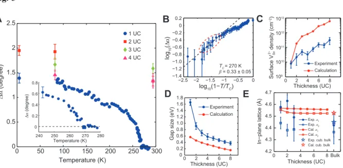
bending, and polarization manipulation by electric field, strongly support the occurrence of ferroelectricity in the 1 UC SnTe film. However, all the evidence so far is still at the liquid helium temperature. At higher temperature, the spontaneous polarization P diminishes and eventually disappears at the ferroelectric transition temperatureTc. During the variable
temper-ature measurement, the distortion angle∆α of the rock salt unit cell is conveniently determined by the separation between the two sets of Bragg peaks (Fig. S9). The polarization is then derived through the relation P2
∝ ∆α (32). The temperature dependence of ∆α is plotted in Fig. 3A. For the 1 UC film, ∆α drops as the temperature increases and becomes zero at Tc = 270 K. The critical temperature for 1 UC film is much higher than the bulk value of about
100 K (25). Within the precision of measurement,∆α approaches zero continuously at Tc (see
inset of Fig. 3a), which is in agreement with the behavior for a second order phase transition. The critical indexβ = 0.33 ± 0.05 (P ∼ (Tc −T )β) is extracted by plotting∆α versus T on
a log-log scale (Fig. 3B). The critical exponent here is identical to the value, 0.33, observed in the PbZr0.9Ti0.1O3bulk material (33) and larger than the values of current available two
dimen-sional models with short range interaction, such as 1/8 of 2D Ising model (31). It indicates that long-range correlated microscopic model is required to fully account the observed result here.
For thicker films from 2 to 4 UC,Tc is even higher than the room temperature (RT).
Vari-able temperature STM measurement above RT is beyond the capability of current instrument. However, domain structures and lattice distortion (Fig. S17), as well as the band bending (Fig. S18), have all been observed at RT for 2 to 4 UC films. The evidence for ferroelectric phase at RT also comes from the Raman spectroscopy. Ferroelectric phase transition can be viewed as a condensation of transverse optical (TO) phonon near the Brillouin zone center. The Raman spectroscopy directly probes the TO mode softening in ferroelectrics. For SnTe, the Raman signal is inactive aboveTc because of the crystalline symmetry of the rock salt structure. Below
The spectra of 2 UC SnTe film show that the TO mode persists up to RT with only slightly softening (Fig. S19). For comparison, Tc of the 20 nm thick film extracted from the TO mode
peak shift (Fig. S20) is found to be 130 K and consistent with previous report (23).
Generally speaking, reduced dimensionality leads to lower phase transition temperature. The strong ferroelectricity enhancement in atomic-layer-thick SnTe films is unusual and may have its origin in the lower Sn vacancy density, larger energy gap and expanded in-plane lat-tice. The ferroelectric transition strongly depends on the screening effect of free carriers on the dipole-dipole interaction. For example, the bulk transition temperature of SnTe reaches 100 K only when the carrier density has been reduced to 1020cm−3. Both experiment and density
functional theory (DFT) calculation (Fig. 3C) reveal that the density of Sn vacancies (so the free carriers) drops by 2∼3 order of magnitude in the SnTe ultra-thin film. So a higher Tc is
expected. It is worth to note that the Tc of 1 UC film is lower than that of the2 ∼ 4 UC films,
probably because the effect of reduced dimensionality becomes more prominent in the case of 1 UC. Besides the lower carrier density, larger energy gap also helps to make SnTe thin film less conductive. The bulk IV-VI semiconductors such as SnTe usually have narrow band gaps. However, the gap of SnTe is dramatically increased when the film thickness is less than 8 UC as shown in Fig. 3D. The large band gap may facilitate theTc enhancement.
Both experiment (with slightly large uncertainty) and the DFT calculation suggest that the in-plane lattice constants of SnTe increase when the film becomes thinner (Fig. 3E). The lat-tice constants tune the interactions, including the long-range Coulomb attraction (LRA) and short-range repulsion (SRR), between ions. The LRA tends to drive the ions away from the centrosymmetric positions and favors the ferroelectric phase while the SRR tends to push them back and reduce polarization. LRA and SRR scale as r−3 andr−n(n ∼ 10) (34), respectively,
where r is the distance between a cation and an anion. Therefore, if the lattice expands, SRR is overwhelmed by LRA and ferroelectricity is enhanced. Such mechanism was previously
applied to perovskites to explain the ferroelectric phase in their thin films (12, 35).
Based on the in-plane polarized ferroelectric thin film, a non-volatile ferroelectric random access memory (FeRAM) device (Fig. 4A) can be designed to take advantage of the miniature size and high transition temperature. The voltage pulses VW and VR are applied only during
the writing and reading processes, respectively. The writing voltageVW generates the in-plane
electric field to flip the in-plane polarization of the ferroelectric film. The two opposite direc-tions of polarization represent the ON and OFF states of the memory unit. The states are read by electron tunneling into an edge driven by the voltageVR. The tunneling currentItstrongly
depends on the band bending. The dependence can be easily understood by the band structure on the edges (see the schematic in Figs. 4B, 4C). To demonstrate the mechanism and simulate the reading process, theI −V curves (Fig. 4D) on the edges of a 3 UC SnTe film were measured by STM. During the measurement, the gap distance between tip and sample was fixed. From 0.5 to 0.7 eV, the ON/OFF ratio can reach as high as 3000 (Fig. 4E). Similar measurement is also performed on 1 UC film, which shows much lower ON/OFF ratio. Compared with the con-ventional FeRAM, where reading is destructive, the memory based on the in-plane polarization and tunneling does not reverse the polarization and is non-destructive. Moreover, the fact that the ferroelectricity and band bending could exist in the SnTe nanowire of only 16 nm width (Fig. S22) shows the potential to fabricate devices with high density.
References and Notes
1. K. Novoselov, et al., Nature 438, 197 (2005).
2. Y. Zhang, Y.-W. Tan, H. L. Stormer, P. Kim, Nature 438, 201 (2005). 3. A. Gozar, et al., Nature 455, 782 (2008).
5. W. D¨urr, et al., Phys. Rev. Lett. 62, 206 (1989).
6. M. Farle, K. Baberschke, Phys. Rev. Lett. 58, 511 (1987). 7. X. Xi, et al., Nature Nanotechnol. 10, 765 (2015).
8. M. M. Ugeda, et al., arXiv preprint arXiv:1506.08460 (2015).
9. T. Tybell, C. H. Ahn, J.-M. Triscone, Appl. Phys. Lett. 75, 856 (1999). 10. D. D. Fong, et al., Science 304, 1650 (2004).
11. D. D. Fong, et al., Phys. Rev. Lett. 96, 127601 (2006). 12. D. A. Tenne, et al., Phys. Rev. Lett. 103, 177601 (2009). 13. P. Ghosez, K. M. Rabe, Appl. Phys. Lett. 76 (2000). 14. J. Junquera, P. Ghosez, Nature 422, 506 (2003). 15. Z. Wu, et al., Phys. Rev. B 70, 104108 (2004).
16. N. Sai, A. M. Kolpak, A. M. Rappe, Phys. Rev. B 72, 020101 (2005). 17. N. Sai, C. J. Fennie, A. A. Demkov, Phys. Rev. Lett. 102, 107601 (2009).
18. Y. Zhang, G.-P. Li, T. Shimada, J. Wang, T. Kitamura, Phys. Rev. B 90, 184107 (2014). 19. E. Almahmoud, I. Kornev, L. Bellaiche, Phys. Rev. B 81, 064105 (2010).
20. A. V. Bune, et al., Nature 391, 874 (1998).
21. J. O. Dimmock, I. Melngailis, A. J. Strauss, Phys. Rev. Lett. 16, 1193 (1966). 22. N. Wang, et al., Phys. Rev. B 89, 045142 (2014).
23. S. Sugai, K. Murase, H. Kawamura, Solid State Commun. 23, 127 (1977).
24. W. Jantsch, Dielectric properties and soft modes in semiconducting (Pb, Sn, Ge) Te (Springer, 1983).
25. K. L. I. Kobayashi, Y. Kato, Y. Katayama, K. F. Komatsubara, Phys. Rev. Lett. 37, 772 (1976).
26. M. Iizumi, Y. Hamaguchi, K. F. Komatsubara, Y. Kato, J. Phys. Soc. Japan 38, 443 (1975). 27. T. H. Hsieh, et al., Nature commun. 3, 982 (2012).
28. Z. Sheng, N. Ogawa, Y. Ogimoto, K. Miyano, Adv. Mater. 22, 5507 (2010). 29. V. Garcia, et al., Nature 460, 81 (2009).
30. J. L. Giocondi, G. S. Rohrer, Top. Catal. 49, 18 (2008).
31. M. E. Lines, A. M. Glass, Principles and applications of ferroelectrics and related materi-als(Oxford University Press, 1977).
32. R. Clarke, Phys. Rev. B 18, 4920 (1978).
33. R. Clarke, A. M. Glazer, J. Phys. C: Solid State Phys. 7, 2147 (1974). 34. G. A. Samara, T. Sakudo, K. Yoshimitsu, Phys. Rev. Lett. 35, 1767 (1975). 35. K. J. Choi, et al., Science 306, 1005 (2004).
Acknowledgements
We thank H. J. Xiang, Y. G. Zhao, P. Yu, G. M. Zhang and B. F. Zhu for discussions. We thank Y. Wang for sample characterization by transition electron microscope. The work is financially supported by National Natural Science Foundation and Ministry of Science and
Technology of China. Q. M. Z. was supported by the Ministry of Science and Technology of China (973 projects 2012CB921701 and 2011CBA00112) and the NSF of China. J.W.L and L.F were supported by the DOE Office of Basic Energy Sciences, Division of Materials Sciences and Engineering under Award No. DE-SC0010526.
Figure Captions
Fig. 1, structure and lattice distortion of SnTe film.
A,Schematics of the SnTe crystal structure (upper) and the SnTe film (lower).
B, Typical STM topography image of SnTe film (sample bias 3.0 V, tunneling current 30 pA, temperature 4.7 K). The dotted line in red indicates the steps of substrate.
C, dI/dV spectra acquired on the surface of a 1 UC film at 4.7 K. The dI/dV of conduction and valence bands has large difference in intensity. For clarity, the spectra above and below the Fermi level are measured under different tunneling conditions: 3.0 V, 100 pA above and −0.5 V, 100 pA below. The arrows indicate the edges of the valance and conduction bands, respectively.
D, The stripe domain of a 1 UC SnTe film (imaging conditions: −0.2 V, 30 pA, 4.7 K). The arrows in each domain indicate the direction of lattice distortion. Upper inset: topography image across a domain boundary (−0.2 V, 100 pA). Lower inset: the graphene substrate (−0.1 V, 200 pA).
E, Fourier transform (left) of an area (inset, 4.7 K) crossing a domain boundary. The Bragg peaks are associated with the Te sublattice. The parallel lines in the inset indicate the moir´e stripes in each domain. The atomically-resolved image right on the domain boundary is shown in Fig. S6(b). The Te(10) peaks for the whole image, the left domain and the right domain are enlarged in the right panels, respectively.
F, Schematic of the lattice distortion and atom displacement in the ferroelectric phase. The solid lines indicate the rock salt unit cell and the dashed lines indicate the primitive cell of the Te sublattice. The arrows point to the directions of distortion. aL1, aL2, aR1 and aR2 are the basis of the primitive cell, and∆α is the distortion angle of the rock salt unit cell.
Fig. 2, band bending induced by spontaneous polarization and manipulation of the
do-main walls.
A,Schematics showing the band shift of a bulk ferroelectric with and without internal screening charge.
B,The apparent height of edge. If an edge is negatively charged (top panel), more states between EF and eVs are available for tunneling. Therefore the STM tip has to be lifted up to keep a
constant current during scanning, giving rise to a higher apparent height. The positively charged edge has the opposite trend.
C, Spatially resolved dI/dV spectra obtained along the two arrows in the image (1 UC, 3.0 V, 100 pA, 4.7 K) on the left.
D, Image of a 1 UC single domain island (−0.2 V, 100 pA, 4.7 K). The polarization is un-ambiguously determined to be along the [110] direction. The image is a combination of nine smaller scans. The “+” and “−” signs on the edges indicate the positive and negative polariza-tion charges.
E,Topography images (−0.2 V, 50 pA, 4.7 K) of the same area before (upper) and after (lower) a voltage pulse is applied on the 1 UC film. The arrows indicate the direction of polarization.
Fig. 3,Tc enhancement in the1 ∼ 4 UC SnTe films.
A, Temperature dependence of the distortion angle for the 1 ∼ 4 UC SnTe films. Inset: the distortion angle near Tc = 270 K for the 1 UC film exhibiting the behavior of a second-order
phase transition. The2 ∼ 4 UC films show significant distortion even at room temperature. B, Power-law fitting of the data for 1 UC SnTe film near Tc. The critical exponent of P is
derived using the approximation P2
∝ ∆α. The ellipse with red dash line indicates the data points for linear fitting.
D, Experimentally measured and DFT calculated thickness dependence of the electronic band gap.
E, Thickness dependence of the lattice constants determined by experiment data and DFT cal-culation.
Fig. 4, non-volatile memory device based on the ferroelectric tunnel junction with in-plane
polarization.
A, Schematic of the device structure. VRandVW are the reading and writing voltages;Itis the
tunneling current.
B, Band diagram of the tunneling process between the ferroelectric thin film and a top electrode. µ is the chemical potential of the film. For the positively (negatively) charged state, a threshold voltageVR= Ec+/e (Ec−/e) is needed to open the tunneling channel between the top electrode
and the conduction band of the edge.
C, Threshold voltages measured by STM. For a 3 UC film,E+
c andEc−are measured by dI/dV
(set point: 1.0 V, 100 pA) and found to be 0.36 eV and 0.76 eV, respectively.
D, Simulation of the reading process by STM. When the tip moves from one edge to another, the feedback loop of STM is turned off to maintain the same distance of tunneling junction. The tunneling current increases rapidly after the bias voltage reaches the corresponding threshold E+
c /e or Ec−/e. Large ON/OFF ratio is achieved between E +
c /e and Ec−/e.
Fig. 1 A B C [001] [100] [010] 50 nm` P 1 UC SnTe Graphene 1.05 0.95 −0.9 −1.0 1.05 0.95 1.05 0.95 −0.9 −1.0 −0.9 −1.0 Whole image Left domain Right domain 2 nm 1 nm Te Sn [010] [100] −1.5 −1 −0.5 0 0.5 1 1.5 −1.5 −1 −0.5 0 0.5 1 1.5 qy ( Å -1) q x (Å -1) Te (10) Te (01) Te (10) Te (01) [010] [100] 30 nm P Dom P a in w a ll 100 nm ∆α L1 a L2 a ∆α Domain wall R1 a aR2 R × o Graphene 6H-SiC 1 UC SnTe −0.5 0 0.5 1 1.5 2 Sample bias (V) d I/d V (a .u .) D E F 2 UC 2 UC 1 UC Graphene [010] [100]
Fig. 2
A
B
10 nm + + + + + + + + + [010] [100]P
− − − − − − − − − Sa mp le b ia s (V) 1.9 1.8 1.7 1.6 1.5 Distance (nm) 0 5 10 15 20 25 30 35 Distance (nm) Sa mp le b ia s (V) 0 5 10 15 20 25 30 35 1.7 1.6 1.5 1.4 1.3 40 nmC
D
50 nmE
E C E V x P P x E C E V −Without screening With screening
− − − − − + + + + + + − − − − − − + + + + + + +++ + ++ − − − − − − Up Down d I/d V (a .u .) High Low E F eV S E F eV S E V E V I t I t
Fig. 3 A B C D E 0 50 100 150 200 250 300 0 0.5 1 1.5 2 2.5 Temperature (K) ∆ α (d e g re e ) 1 UC 2 UC 3 UC 4 UC 240 250 260 270 280 0 0.2 0.4 0.6 0.8 Temperature (K) ∆ α (d e g re e ) Thickness (UC) G a p si ze (e V) 2 4 6 8 0 0.2 0.4 0.6 0.8 1.0 1.2 1.4 1.6 1.8 0 Calculation Experiment 0 2 4 6 8 109 1010 1011 1012 1013 Thickness (UC) Su rf a ce VSn d e n si ty (cm −2) Calculation Experiment 2 − 0 2 4 6 8 4.2 4.3 4.4 4.5 4.6 4.7 Bulk Cal. a1 Cal. a2
Cal. cub. bulk Exp. a1 Exp. a2
Exp. cub. bulk
Thickness (UC) In −p la n e la tt ice ( Å) −2.5 −2 −1.5 −1 −0.5 0 −1.4 −1.2 −1.0 −0.8 −0.6 −0.4 −0.2 0.2 log10(1−T/TC) lo g10 (∆ α ) T C= 270 K β = 0.33 ± 0.05 0
Fig. 4
Ferroelectric semiconductor
Large band gap insulator
Substrate P Top electrodes Graphene V R V W A I t
A
B
C
10−6 10−4 10−2 100 102 T u n n e lli n g cu rre n t (n A) I ON I OFF 10−2 100 102 104 IO N /IO F F 0 0.2 0.4 0.6 0.8 1 Sample bias (V) 103 101 10−1 eV R µ e– GND E C E V + + E C EC GND + − µ GND E C E V + + µ GND E C E V − − eV R µ GND E C E V − − 10−3 10−2 10−1 100 101 d I/d V (a .u .)Positive polarization charge without bias voltage
Positive polarization charge with bias voltage
Negative polarization charge without bias voltage
Negative polarization charge with bias voltage
e–
D
Supplementary Materials for
Discovery of robust in-plane ferroelectricity in
atomic-thick SnTe
Kai Chang, Junwei Liu, Haicheng Lin, Na Wang, Kun Zhao,
Anmin Zhang, Feng Jin, Yong Zhong, Xiaopeng Hu, Wenhui Duan,
Qingming Zhang, Liang Fu, Qi-Kun Xue, Xi Chen,
†Shuai-Hua Ji,
‡†Corresponding author. E-mail: xc@mail.tsinghua.edu.cn(X.C.)
‡Corresponding author. E-mail: shji@mail.tsinghua.edu.cn(S.-H. J.)
November 12, 2015
This PDF file includes: Materials and Methods Supplementary Text Figs. S1 to S22 Full Reference List
1
Materials and Methods
1.1
Sample preparation and characterization
The strain-free SnTe films were grown on the n-doped 6H-SiC(0001) substrate terminated with epitaxial monolayer or bilayer graphene. The SiC substrate was annealed under Si flux at 850
∼ 950◦C for at least 10 min to form a Si-rich surface with(3 × 3) reconstruction, and then
heated up to 1400◦C for 10 min to make the surface graphitize. The surface of the substrate is
covered by monolayer/bilayer graphene after the treatments. The growth and characterization of the SnTe samples were performed on a Unisoku system combining low-temperature STM and
molecular beam epitaxy, whose base pressure is1×10−10Torr. SnTe molecules were evaporated
from a BN crucible. The temperature of source is 450◦C, giving rise to a slow growth rate of
∼ 2.5 UC per hour. The substrate temperature varies from room temperature to 200◦C. Low substrate temperature leads to fractal growth, forming terraces and islands with irregular edges, and the film thickness is relatively uniform. In contrast, the islands grown under high substrate temperature have straight edges, and the film thickness varies between islands. The large area
1 UC films in the main text were obtained under substrate temperature of 130 ∼ 180◦C, while
the films for Raman experiments were grown under ∼ 50 ◦C. Both the Reflective High Energy
Electron Diffraction (RHEED) pattern and STM topography reveal polycrystalline nature of the film, as Fig. S1 shows. The Van der Waals bonding between the film and the substrate is evidenced in Fig. S2, in which a 200 nm × 100 nm sized island drifts on the substrate smoothly. After the growth, the samples were immediately transferred into the STM without taking out of the ultra-high vacuum environment. The STM uses Pt-Ir alloy tips modified and checked
on the surface of Ag(111) islands. The dI/dV spectra were recorded with a Signal Recovery
lock-in amplifier with the modulation frequency 913 Hz. The variant temperature experiments were performed between liquid nitrogen temperature and room temperature. At the beginning,
the dewar was filled with liquid nitrogen, and stayed stable for at least two days to let all the components cool down sufficiently. Then we blew the liquid nitrogen out and let the whole system warm up naturally. The thermal shield of the STM is good enough to keep the heating
process slower than 15 K per day, which leads to an acceptable lateral thermal drift of<40 nm
per hour. During the whole heating process, we scanned the sample at least once in every 4 hours. Thermal drift during the waiting time was compensated by manually moving the XY stage of the STM. All the data in one dataset was collected from the same area. As Fig.
S3 shows, the domain wall disappears when the temperature is higher than Tc. The variant
temperature experiment was repeated 3 times, and the results are well reproducible.
The thickness was determined by the combination of the STM topography and first-principle calculations. Since the local density of states of SnTe films and the graphene substrate are
different, the height of the film edges are not exactly the integer multiply of 6.32 ˚A. As Fig.
S4 shows, the height of 0.75 nm could be either 1 UC or 1.5 UC, and the height of 1.38 nm could be either 2 UC or 2.5 UC. However, the height of the step between two SnTe terraces is exactly 0.63 nm. When the thickness of the film is lower than 5 UC, the height of the SnTe steps is always 0.63 nm, which implies that the thickness of all the films should be odd or even atomic layers. In order to unambiguously determine the thickness, we calculated the surface formation energy of the films with different thickness. The surface formation energy is defined as ES = [E0,F −E0,B ·d]/S, where E0,F is the total energy of the film with the thickness of
d, E0,B is the total energy of one atomic layer in bulk SnTe, and S is the surface area of the
film. The lattice constants are relaxed to the lowest energy. The method of calculation will be further explained in section 2.5. The result shows oscillation behavior: the formation energy of an even-atomic-layer thickness is lower than the neighboring odd-atomic-layer thicknesses. Therefore, our SnTe films should have the thickness of even atomic layers, i.e., integer unit cells.
The defect density was determined by counting the Sn vacancies at the topmost atomic layer in the experiments. Both the results from experiments and calculations were converted into the two-dimensional density of a single atomic layer. Fig. S5 shows an example of the STM topography of a 6 UC film. The bright defects are identified as Sn vacancies in the topmost atomic layer, which has negative charge and locally bend the bands upwards. Some dim defects can also be seen in the image, which are probably the Sn vacancies beneath the topmost layer.
1.2
Fourier transformation analysis
The original image of Fig. 1E (main text) is shown in Fig. S6, which contains two domains. Its Fourier transformed image shows 3 types of spots, 1) quasi-square shaped spots at larger
q, 2) hexagonal shaped spots at small q and 3) some other irregular spots at small q, as Fig.
S6 indicated. Spots 1) are obviously from the quasi-square SnTe lattice quasi-square lattice.
The hexagonal spots 2) correspond to the(6 × 6) superstructure in the buffer layer of the SiC
substrate with |q| = 0.39 ˚A. The irregular spots 3) come from the moir´e pattern between the
quasi-square SnTe lattice and hexagonal graphene lattice. The simulation of the moir´e pattern is shown in Fig. S7.
Apparently, each dot of SnTe has split into two (as well as the spots from moir´e pattern) in Fig. 1E (main text). We split the original figure into two parts along the domain wall, and
performed FT respectively on them. The q axes were recalculated based on the size of each
part. The FT results reveal the origin of the splitting, as Fig. 1E (main text) shows.
The lattice parameters of the distorted SnTe lattice were determined from the FT images. All
the FT images are corrected by the spots of the(6 × 6), which act as a natural in situ reference
system.
The distortion angle∆α of the rock salt unit cell can be determined in better precision than
calculated by ∆α = saRS/2, in which s is the splitting of the spots and aRS = 6.32 ˚A is the lattice constant of the undistorted rock salt unit cell, an acceptable approximation within the resolution of the instrument. As Fig. S9 shows, although the spots are broadened along the slow-scan direction, the resolution along the fast-scan direction is still good. The fast-scan direction was kept parallel with one base of the rock salt unit cell in all the images. When
the temperature is close to Tc, the splitting becomes smaller and smaller. In order to correctly
identify the spots, we performed FT on each domain and measured the (lateral) coordinates of the spots respectively.
One may have noticed that the splitting of the Te(10) spots is a little larger than the Te(01) spots in Fig. 1E (main text). This is the result of the nonlinear response of the piezoelectric scanner. As shown in Fig. S10, when the fast-scan direction is reversed, the magnitude of the splittings of Te(10) and Te(01) is also exchanged. A simple method to correct this error is to average the splitting values measured from the images with opposite fast-scan directions.
Since moir´e pattern is very sensitive to the change of the lattice parameters of SnTe, the splitting of the spots from moir´e pattern is even larger than the spots from SnTe lattice in the FT images. Fig. S11 clearly shows how the split moir´e pattern spots getting closer as the
temperature increases, and finally merging with each other aboveTc.
1.3
Determining the polarization direction of each domain
In order to determine the polarization direction of each domain, we first measure the lattice parameters within each domain to decide along which direction the lattice is elongated. There are only two possibilities once the elongating direction is fixed. Then we refer to the band bending at the edge of the island to fix the polarization direction. Fig. S12 shows an example of determining the polarization directions of the domains in Fig. 1D (main text).
2
Supplementary Text
2.1
1 UC PbTe film
For comparison, no band bending is observed in 1 UC PbTe film as shown in Fig. S13, which has identical NaCl structure and very similar electronic structure with paraelectric SnTe films. Both the bulk material and films of PbTe are paraelectric. This result further supported that the band bending in SnTe films is induced by spontaneous polarization.
2.2
The domain walls in 1 UC SnTe film
Most of the domains in 1 UC SnTe film are 90◦ domains, as Fig. 1D (main text) and Fig. S14.
This is quite different from the usual ferroelectrics, in which 180◦ domain walls dominate. This
can be understood from the two-dimensional nature of the 1 UC film, in which the polarization charges distribute on a line at the edge, rather than on a plane as in bulk ferroelectrics. When no screening is considered, the depolarization field in a two-dimensional ferroelectric film
de-cays with Ed ∝ x−1, thereby the electric potential varies with ϕ ∝ ln(x/λ), in which λ is a
feature length. In contrast, the depolarization field does not decay at all in bulk ferroelectrics
without screening. In realistic films, Eddecays faster than logarithmic function because of the
screening effect of the conducting substrate and finite carrier density in the film. Our spatially
resolved dI/dV spectra imply exponential decay of the electric potential. As Fig. S15 shows,
the depolarization field only influences the region ∼20 nm away from the edge. Therefore, it is
not necessary to form 180◦domains, which lower depolarization energy but have higher domain
wall energy than 90◦domains.
In fact, 180◦ and 90◦wedge-shaped domain walls are occasionally observed in 1 UC SnTe
2.3
Room temperature ferroelectricity of 2∼4 UC SnTe films
The domain walls and the splitting of the SnTe Bragg spots of 2∼4 UC SnTe films at room
temperature are shown in Fig. S17. Although it is difficult to measure dI/dV spectra at room
temperature, the band bending of 2∼4 UC SnTe films can still be revealed from the topography images collected at certain bias, as Fig. S18 shows.
2.4
Raman spectroscopy
Confocal micro-Raman measurements were performed in a backscattering configuration using a Jobin Yvon HR800 single-grating-based micro-Raman system equipped with a volume Bragg grating low-wavenumber suite, a liquid-nitrogen cooled back-illuminated CCD detector and a 633 nm laser (Melles Griot). The laser was focused onto the samples with a spot size of 510
µm2
. The laser power was maintained at a level of 1 mW and monitored with a power meter (Coherent Inc.).
The Raman spectroscopy directly probes the TO mode softening in ferroelectrics. For SnTe,
the Raman signal is inactive above ferroelectric transition temperatureTc because of the
crys-talline symmetry of the rock salt structure. BelowTc, the TO mode becomes Raman active and
its frequency is given byωT O ∝ (Tc −T )1/2(1). The Raman spectra from a sample with the
thickness of ∼20 nm reveals the softening of the TO mode (Fig. S20). The Tc of the 20 nm
thick extracted from the TO mode peak shift (Fig. S20) is found to be 130 K and consistent with previous report (1).
The ultra-thin film for Raman experiments were grown at the substrate temperature of
∼50◦C to make it as uniform as possible. As Fig. S19 shows, 66% area of our sample was
covered by the 2 UC SnTe thin film, which would contribute most signal for the Raman spectra.
As the spectra in Fig. S19 indicate, peak appears at ∼46.8 cm−1at 10 K (the background of
magnitude. The peak position shifts to the higher energy comparing with the ∼ 26.8 cm−1 Raman shift of 20 nm thick film. This shift is consistent with the conclusion from STM,
which indicates the Tc should be higher than room temperature. By the rough estimation from
ωT O ∝(Tc−T )1/2, the transition of 2 UC film should be around 400 K. The measurement also
has been performed on 1 UC thin film with nearly 50% coverage. However, even with half hour integration time, no signal could be detected in our current instrument, which may come from the relatively weak polarization and reduced thickness. The specific reason is unclear in current stage.
2.5
First-principles calculations
All the first-principles calculations are based on density functional theory as implemented in the Vienna ab initio simulation package (VASP) (2, 3), by using the Perdew-Burke-Ernzerhof (PBE) generalized gradient approximation (4) and the projector augmented wave potential (5).
We use (001) slab model up to 8 UC with 10 ˚A vacuum layer to study the lattice distortion
varying with the thickness. The corresponding Monkhorst-Pack k mesh is16 × 16 × 1, and the
convergence are tested up to 26 × 26 × 1. The energy cutoff of the plane-wave basis is 400
eV. The crystal structures are fully optimized with forces converged to less than 0.001 eV/ ˚A.
The polarizations were calculated using the modern theory of polarization (6) as implemented in VASP.
During growth (substrate temperature 180◦C), SnTe is highly possible to exist in the
rock-salt structure, thus we constrain our defect study within the rock-rock-salt structure and take3 × 3
in-plane supercell with single defect at different depth to study the defect formation. The formation energy of defects is calculated as (7, 8)
∆H[Xq] = Etot[Xq] − Etot[per] + µSn+ q(Ev+ ∆V ), (1)
one defectX and without a defect, respectively. µSnis the chemical potential of the elemental bulk Sn (diamond cubic phase of Sn (9)), representing Sn-rich condition as Te can easily form
Te2 gas desorbing from the surface. q is the charge on the defect, and Ev, in our expressions
for formation energies of charged states, is chosen to be the VBM of the perfect slab. ∆V is to
align the reference potential in our defect supercell with that in the bulk (7, 8) which has been found to be very small (∼0.01 eV). Moreover, the error associated with charged defect-defect interaction (10, 11) has been tested to be smaller than 0.01 eV and can be safely ignore. The
de-fect concentration can be calculated by the Boltzmann distributionnV = NSnexp(−EV/kBT )
, in whichN = 5 × 10¹⁴
cm−2is the density of Sn sites,EV is the vacancy formation energy,kB
is the Boltzmann constant andT is the substrate temperature of growth. One can refer to Phys.
Rev. B 89, 045142 (2014) for more information on the calculation of defect formation energy in
the bulk materials. And the formation energy of thin films is defined as the total energy of the thin films minus the corresponding bulk energy (12, 13).
2.6
The lateral size of the device
Due to the high quality of the film, band bending is robust even if the size of the island is small. Since the depolarization field only influences the region ∼20 nm inside the edge, the magnitude of band bending is not likely to decrease until the island width is smaller than ∼40 nm. Fig. S22 shows an example of a 3 UC SnTe island with the width of only 16 nm. The band bending across this island is larger than 0.4 eV. Therefore, such atomic-thick ferroelectric islands are compatible with the miniaturized device size in modern electronics.
References and Notes
1. S. Sugai, K. Murase, H. Kawamura, Solid State Commun. 23, 127 (1977). 2. G. Kresse, J. Furthm¨uller, Computational Materials Science 6, 15 (1996).
3. G. Kresse, J. Furthm¨uller, Phys. Rev. B 54, 11169 (1996).
4. J. P. Perdew, K. Burke, M. Ernzerhof, Phys. Rev. Lett. 77, 3865 (1996). 5. P. E. Bl¨ochl, Phys. Rev. B 50, 17953 (1994).
6. R. D. King-Smith, D. Vanderbilt, Physic. Rev. B 47, 1651 (1993). 7. C. G. Van de Walle, J. Neugebauer, J. Appl. Phys. 95, 3851 (2004). 8. N. Wang, et al., Phys. Rev. B 89, 045142 (2014).
9. R. W. G. Wyckoff, Crystal structures, vol. 1 (Interscience New York, 1960). 10. H.-P. Komsa, A. Pasquarello, Phys. Rev. Lett. 110, 095505 (2013).
11. C. Freysoldt, J. Neugebauer, C. G. Van de Walle, Phys. Rev. Lett. 102, 016402 (2009). 12. J. Wang, et al., Phys. Rev. B 89, 125308 (2014).
Figures of Supplementary Materials
Fig. S1. The RHEED pattern and STM topography of the polycrystalline SnTe films. a, RHEED patterns of the substrate (upper) and the as-grown SnTe film (lower). The average thickness of the SnTe islands is more than 10 UC when no stripe from the substrate appears any more. The SnTe stripes on the RHEED pattern can be seen from any incidental azimuth, imply-ing that the in-plane orientations of the SnTe islands are random. b, Several STM topography images of the SnTe films. All the images have the same size 500 nm × 500 nm. The substrate
Fig. S2.
1 UC SnTe island with the size of about 200 nm × 100 nm. Tunneling conditions: 3.0 V, 20 pA. The island can be moved by the STM tip.
Fig. S3.
The domain wall disappears when the temperature is higher thanTc. All the images are acquired
from the same area, which can be confirmed by the distribution of the bright spots (defects on the
substrate). Thermal drift has been corrected according to the hexagonal(6 × 6) superstructure
on the substrate. Tunneling parameters: left, −0.5 V, 10 pA; middle, −0.2 V, 20 pA; right,
−0.1 V, 30 pA. 2 3 4 5 6 7 8 9 10 11 12 12 14 16 18 20 22 24 26
Number of atomic layers
Su rf a ce fo rmat ion e n erg y (me V/ Å 2) Undistorted lattice Distorted lattice 0.75 nm 0.63 nm 1.38 nm a 100 nm b Fig. S4.
Determining the thickness of the SnTe films. a, STM topography of the SnTe film. The height of the steps are labeled. b, the surface formation energy of SnTe films with different thickness, calculated by density functional theory.
Fig. S5.
The Sn vacancies at the surface of a 6 UC film. a, STM topography of a 100 nm × 100 nm area. b, a 10 nm × 10 nm zoom-in image of a single defect. The tunneling condition of both
the images is −0.2 V, 20 pA.
Fig. S6.
The spots in the Fourier transformed images. a, the same STM image as the inset of Fig. 1e
square in the left figure. c, the Fourier transformed image of a. The quasi-square spots from
SnTe lattice and the hexagonal spots from SiC-(6 × 6) superstructure are indicated.
Fig. S7.
The simulation of the moir´e pattern. a, the same STM image as the inset of Fig. 1e (main text). b, the FT image of the left-domain in a. c, the simulated moir´e pattern, with lattice parameters
a1S = 4.6 ˚A, a2S = 4.4 ˚A for SnTe anda1G = a2G = 2.46 ˚A for graphene. The angle between
a1S and a1G is 50◦. The fluctuation induced by the SiC-(6 × 6) superstructure, whose basis
rotate 30◦ about that of graphene, is also superposed. d, the FT image of c. e, the FT image
of the right domain in a. f, the simulated moir´e pattern with a1S = 4.4 ˚A, a2S = 4.6 ˚A and
Fig. S8.
A schematic drawing explaining how the distortion angle is calculated from the splitting of the SnTe spots. The red and blue parallelograms represent the SnTe spots from the left- and right-domain, respectively.
Fig. S9.
The splitting of the Te(10) spots at different temperature. The thermal drift has been corrected
according to the hexagonal spots from the(6 × 6) superstructure. All the images are in the same
Fig. S10.
The FT images from two atom resolved topography images recorded at the same time, with opposite fast-scan directions.
Fig. S11.
The splitting of the moir´e pattern spots at different temperature. The thermal drift has been
Fig. S12.
Determining the polarization direction of each domain. a, STM topography the same as Fig. 1b. The letters U, D and N stand for upward, downward and no obvious band bending, respectively. b, the lattice parameters of the domains 1∼6 indicated in a. The basis along [110] and [110]
are elongated alternatively. These lattice parameters have not been corrected by the (6 × 6)
superstructure because only the relative magnitude is cared here.
Fig. S13.
There is no band bending at the edge of a paraelectric 1 UC PbTe island. PbTe is grown on the same substrate as SnTe films and shows the same growth mode. The left panel shows the
typical image of PbTe film (550 nm × 550 nm, 3.0 V, 20 pA, 4.7 K). The spatially resolved dI/dV (right panel) along the line perpendicular to the edge of a 1 UC PbTe island shows no
bending.
Fig. S14.
The domains in a large 1 UC island. The images are acquired under −0.2 V and 20 pA.
Deriva-tive mode is used to display the images so that the domain walls can be clearly seen. The arrows
indicate the directions of polarization. Note that almost all the domains are 90◦. The two steps
0 5 10 15 20 25 30 35 40 1.55 1.6 1.65 1.7 1.75 1.8 Sa mp le b ia s (V) Distance (nm) 0 5 10 15 20 25 30 35 40 1.25 1.2 1.35 1.3 1.45 1.5 1.55 1.6 1.65 Distance (nm) Sa mp le b ia s (V) Fig. S15.
Fitting the band bending profiles near the edges of a 1 UC SnTe film by an exponential model:
V = ae−x/λ + c. Left: a = 0.198 V, λ = 4.85 nm, c = 1.57 V; right: a = −0.329 V,
λ = 6.12 nm, c = 1.57 V. The red circles are the energies of the DOS peak near CBM, and the
Fig. S16.
Various types of domain boundaries in the 1 UC SnTe films. a-c, Atomically resolved
topogra-phy images of the domain boundaries (a,b: −0.2 V, 100 pA; c: −0.5 V, 200 pA). The arrows
indicate the directions of polarization. d-f, Fourier transform of the Te sublattices in a-c. g-i,
Fig. S17.
Domains and splitting of the Bragg spots at room temperature. a-c, Topography images of the
domain boundaries for 2 UC (a, −30 mV, 100 pA), 3 UC (b, −30 mV, 20 pA) and 4 UC (c,
−50 mV, 2.0 nA) SnTe films, respectively. d-f, Fourier transform of a-c.
Fig. S18.
Band bending on the edges of 2∼4 UC SnTe islands at room temperature. The [100] and [010] edges are alternatively bright and dark, implying upward and downward band bending. The [110] edges are always bright because of the existence of dangling bonds. The tunneling
parameters are −0.2 V, 10 pA for a and b, and −0.1 V, 10 pA for c. The brightness of the
straight [110] edges do not obey the polarization direction because of the imbalanced local charge, i.e., the [100] edges has alternatively arranged Sn and Te atoms, while the [110] edge
have only one type of atoms. 25 50 75 100 In te n si ty Raman shift (cm-1) 10 K 20 K 40 K 60 K 80 K 100 K 120 K 140 K 160 K 180 K 200 K 220 K 240 K 260 K 280 K 300 K 2 2 2 2 2 2 2 2 2 2 2 2 2 2 3 3 3 3 3 3 3 2 1 S S S S S S >3 >3 >3 >3 >3 a b 100 nm Fig. S19.
The Raman spectroscopy experiment on a SnTe film, whose thickness is dominated by 2 and 3 UC. a, the STM topography of the sample. Film thickness has been labeled on the image, in
which “S” stands for substrate. The percentage of the substrate, 1 UC, 2 UC, 3 UC and>3 UC
films are 12%, 2%, 66%, 13%, and 7%, respectively. b, Raman spectra of this film. The TO
mode at ∼ 46.8 cm−1 persists up to room temperature. The peak position of the TO mode in
the Raman spectra shifts slightly as temperature increases from 10 K to room temperature.
0 20 40 60 80 100 120 140 0 100 200 300 400 500 600 700 800 (T O -p h o n o n e n e rg y) 2 (cm -2) T (K) 20 40 60 80 100 300 K 280 K 260 K 240 K 220 K 200 K 180 K 160 K 140 K 120 K 100 K 90 K 80 K 70 K 60 K 50 K 40 K 30 K 20 K 10 K In te n si ty ( a rb . u n its ) Raman shift (cm-1) TO mode ~ 130 K Fig. S20.
Raman spectra of a ∼ 20 nm thick SnTe film. The TO mode at ∼ 27 cm−1 shows softening
as the temperature increases. Usingω2
T O ∝(Tc −T ), the transition temperature Tc ∼130 K is extracted from the fitting.
0 2 4 6 8 0.015 0.02 0.025 0.03 0.035 0.04
Film thickness (UC)
a1 − a2 ( Å) 0 2 4 6 8 12 14 16 18 20 22
Film thickness (UC)
Po la ri za tio n ( µ C /cm -2) Fig. S21.
The calculated spontaneous polarization and lattice distortion of SnTe films. The polarization is defined as the polarization charge divided by the area of the cross section of the film.
Fig. S22.
The band bending of a narrow 3 UC SnTe island. a, the STM topography of the island (−200 mV,
20 pA). The width of this island is 16 nm. b,c, the spatially resolveddI/dV spectra in the
con-duction band and nearEF, acquired along the arrow in a. The white dashed lines indicate the
edge. The total band bending is over 400 meV across the island.
![Fig. 2 A B 10 nm++++ + + + ++[010] [100] P−− − − − − −−− Sample bias (V) 1.91.81.71.61.5 Distance (nm)05 10 15 20 25 30 35 Distance (nm)Sample bias (V)05 10 15 20 25 30 351.71.61.51.41.340 nmC D 50 nmEECEVxPPxECEV−](https://thumb-eu.123doks.com/thumbv2/123doknet/14748006.578913/18.892.117.790.184.653/fig-sample-bias-distance-distance-sample-bias-nmeecevxppxecev.webp)