ATAC: A 1000-Core Cache Coherent Processor with
On-Chip Optical Network
by
George Kurian
Submitted to the Department of Electrical Engineering and Computer
Science
in partial fulfillment of the requirements for the degree of
Master of Science
at the
MASSACHUSETTS INSTITUTE OF TECHNOLOGY
September 2010
ARCHNES
MASSACHUSETTS INSTITUTE OF TECKOLOGYOCT D 5 2010
LIBRARIES
@
George Kurian, MMX. All rights reserved.
The author hereby grants to MIT permission to reproduce and distribute
publicly paper and electronic copies of this thesis document in whole or in
part.
Author ....
Certified by
. . . . . ...- . . . . . . .. . .. . . . . ....
Department of Electrical Engineering and Computer Scienc
September 3, 201
..
...
...
..
e
Anant Agarwal
Professor
Thesis Supervisor
/) A ccepted by ...r ...Terry P. Orlando
Chairman, Department Committee on Graduate Theses
ATAC: A 1000-Core Cache Coherent Processor with On-Chip Optical
Network
by
George Kurian
Submitted to the Department of Electrical Engineering and Computer Science on September 3, 2010, in partial fulfillment of the
requirements for the degree of Master of Science
Abstract
Based on current trends, multicore processors will have 1000 cores or more within the next decade. However, their promise of increased performance will only be realized if their in-herent scaling and programming challenges are overcome. Fortunately, recent advances in nanophotonic device manufacturing are making CMOS-integrated optics a reality-interconnect technology which can provide significantly more bandwidth at lower power than conventional electrical signaling. Optical interconnect has the potential to enable mas-sive scaling and preserve familiar programming models in future multicore chips.
This thesis presents ATAC [13], a new multicore architecture with integrated optics, and ACKwise, a novel cache coherence protocol designed to leverage ATAC's strengths.
ATAC uses nanophotonic technology to implement a fast, efficient global broadcast
net-work which helps address a number of the challenges that future multicores will face. ACKwise is a new directory-based cache coherence protocol that uses this broadcast mech-anism to provide high performance and scalability. Based on 64-core and 1024-core simu-lations with Graphite [20] using Splash2, Parsec, and synthetic benchmarks, we show that
ATAC with ACKwise out-performs a chip with conventional interconnect and cache
coher-ence protocols. On 1024-core evaluations, ACKwise protocol on ATAC outperforms the best conventional cache coherence protocol on an electrical mesh network by 78% with Splash2 benchmarks and by 61% with synthetic benchmarks. Energy simulations show that the energy consumption of the ATAC network that assumes aggressive optical tech-nology predictions is 2.24x lower than that of an electrical mesh network. However, with conservative optical technology predictions, the energy consumption of the ATAC network is 1.5 1x higher than that of an electrical mesh network.
Thesis Supervisor: Anant Agarwal Title: Professor
Acknowledgments
I would like to thank Prof. Anant Agarwal for his enthusiatic support towards my research
and all the technical/presentation skills I have learnt from him. I would like to thank Jason Miller for all the discussions I had with him and for his willingness to explain technical details clearly, precisely and patiently to me. I would also like to thank Nathan Beckmann, Harshad Kasture and Charles Gruenwald for all the interesting discussions I had during the Graphite project. I thank Hank Hoffmann, James Psota, David Wentzlaff, Lamia Youseff, Jason Ansel, Cree Bruins and Marco Santambrogio for all the many ways they have con-tributed to my learning process at MIT. I cannot stop thanking my parents and my brother for everything they have been to me thoughout my life and for making me the person I am today.
Contents
1 Introduction 15
2 Optical Devices Background 19
3 Architecture Overview 23
3.1 ONet Optical Network . . . 24
3.2 Cache Subsystem . . . 27
3.3 External Memory Subsystem . . . 27
4 Cache Coherence Protocol 29 4.1 Operation of the ACKwisek Protocol . . . 30
4.2 Silent Evictions . . . 31
5 Power Modeling 33 5.1 Electrical Mesh Network . . . . 33
5.2 ATAC Network . . . . 36 5.2.1 E N et . . . 36 5.2.2 O N et . . . 37 5.2.3 BNet . . . 39 6 Evaluation 43 6.1 Methodology . . . .. 44 6.2 Performance Evaluation. . . . 45
6.2.2 Synthetic Benchmarks . . . . 55
6.3 Energy Evaluation . . . . 59
7 Related Work 65
List of Figures
1-1 ATAC architecture overview
. . . 20
2-1 Optical transmission of a single bit . . . .
3-1 Hub-to-hub communication over the ONet . . .
4-1 Structure of an ACKwisek directory entry . . .
5-1 Electrical Mesh Network connecting 16 tiles
5-2 Routing of a Packet between tile A and tile B 5-3 Electrical Mesh Router Microarchitecture . . .
5-4 ATAC Network Architecture . . . .
. . . 26
. . . 34 . . . . 34
. . . 36
6-1 Performance of Splash2 and Parsec benchmarks when using the DirkNB
protocol on the ANet and EMesh networks. Results are normalized to the
performance of EMesh-Dir2NB. The number of hardware sharers are
var-ied as 2, 3, 4, 8, 16, 32 and 64. The x-axis values take the form benchmark -network. A and E stand for ANet and EMesh networks respectively. . . . .
6-2 Performance of Splash2 and Parsec benchmarks when using the DirkB
pro-tocol on the ANet and EMesh networks. Results are normalized to the
per-formance of EMesh-Dir2NB. The number of hardware sharers are varied
as 2, 3, 4, 8, 16, 32 and 64. The x-axis values take the form benchmark
-network. A and E stand for ANet and EMesh networks respectively. . . . . .
6-3 Performance of Splash2 and Parsec benchmarks when using the ACKwisek
protocol on the ANet and EMesh networks. Results are normalized to the
performance of EMesh-Dir2NB. The number of hardware sharers are
var-ied as 2, 3, 4, 8, 16, 32 and 64. The x-axis values take the form benchmark -network. A and E stand for ANet and EMesh networks respectively. . . . . 47
6-4 Cache miss rates observed when Splash2 and Parsec benchmarks are run using the DirkNB protocol. The number of hardware sharers are varied as
2, 3, 4, 8, 16, 32 and 64... 48
6-5 Percentage of invalidation broadcasts generated due to memory requests at
the directory of a broadcast enabled cache coherence protocol (ACKwisek or D irkB ). . . . 48
6-6 Performance of Splash2 when using the DirkNB protocol on the ANet and
EMesh networks. Results are normalized to the performance of EMesh-Dir2NB. The number of hardware sharers are varied as 2, 3, 4 and 64. The
x-axis values take the form benchmark -network. . . . 52
6-7 Performance of Splash2 when using the DirkB protocol on the ANet and
EMesh networks. Results are normalized to the performance of EMesh-Dir2NB. The number of hardware sharers are varied as 2, 3, 4 and 64. The
x-axis values take the form benchmark -network. . . . 53
6-8 Performance of Splash2 when using the ACKwisek protocol on the ANet
and EMesh networks. Results are normalized to the performance of EMesh-Dir2NB. The number of hardware sharers are varied as 2, 3, 4 and 64. The
x-axis values take the form benchmark -network. . . . 54
6-9 Performance of the synthetic benchmark running on 64 cores with six
dif-ferent combinations of networks and cache coherence protocols. The
6-10 Performance of the synthetic benchmark running on 1024 cores with 4
dif-ferent combinations of networks and cache coherence protocols. The
per-formance is normalized to that of EMesh-Dir4NB. ACKwise4 and Dir4B
protocols perform poorly on a pure electrical mesh with this synthetic bench-mark as discussed in Section 6.2.2. . . . 58
6-11 Energy Comparison of ANet and EMesh networks. The x-axis values take
the form benchmark -network. EMesh, ANet-Agg and ANet-Cons stand for
the EMesh network and the aggressive and conservative ANet networks
respectively. . . . . 62
6-12 Energy Comparison of ANet and EMesh networks. The x-axis values take
the form benchmark -network. EMesh, ANet-Agg and ANet-Cons stand for
the EMesh network and the aggressive and conservative ANet networks respectively. . . . 63
List of Tables
5.1 256-bit wide Electrical Mesh Energy Parameters . . . 34
5.2 Dynamic Energy per bit on a 256-bit wide Electrical Mesh Network. . . . . 36
5.3 128-bit wide ENet (Modified Electrical Mesh) Energy Parameters . . . 37
5.4 Optical Waveguide Losses . . . 37
5.5 On-Chip Laser Power Calculation . . . 37
5.6 ONet Power Components . . . 38
5.7 128-bit wide BNet (Pipelined Broadcast Tree) Energy Parameters. C stands for the number of clusters (C = 64). n stands for the number of tiles in each cluster (n = 16). . . . 40
5.8 Energy/bit computation for the ANet network assuming aggressive optical technology predictions. . . . 41
6.1 Target System Architecture Configuration Parameters . . . 44
Chapter 1
Introduction
The trend in modem microprocessor architectures is clear: multicore is here. As silicon resources become increasingly abundant, processor designers are able to place more and more cores on a chip with massive multicore chips on the horizon. Many industry pundits have predicted manycores with 1000 or more cores by the middle of the next decade. But will current processor architectures (especially their interconnection mechanisms) scale to thousands of cores, and will such systems be tractable to program? This thesis argues that current multicore architectures will be challenged to scale to thousands of cores and introduces ATAC (pronounced R-tack), a new processor architecture that addresses these issues. ATAC integrates an on-chip optical broadcast communication network within a mesh based tiled multicore architecture to significantly improve the performance, energy scalability, and ease of programmability of multicore processors [19, 18].
Although Moore's Law enables increasing numbers of cores on a single chip, the ex-tent to which they can be used to improve performance is limited both by the cost of com-munication among the cores and off-chip memory bandwidth. Although our research is investigating the application of optical technology to both problems, this thesis focuses on the on-chip interconnect challenge. As computation is spread across multiple cores on a chip, distribution of instructions to the cores, and communication of intermediate values between cores account for an increasing fraction of execution time due to both latency and contention for communication resources. The outlook is particularly dismal for applica-tions that require a lot of global communication operaapplica-tions (e.g., broadcasts to maintain
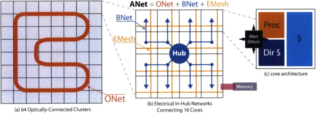
Net = ONet + BNet + EMesh
BNet
O-Net
(c) core architecture
( L ) %etra n- u etVwr s (a) 64 Optically-Connected Clusters Connecting 16 Cores
Figure 1-1: ATAC architecture overview
cache coherence) because each such operation ties up many resources and consumes a lot of energy.
State-of-the-art multicore chips employ one of two strategies to deal with interconnec-tion costs. Small-scale multicores typically use a bus to interconnect cores. This simple design does not scale to large numbers of cores due to increasing bus wire length and con-tention. Another strategy is to use point-to-point networks such as the ring employed by the Cell processor [22]. This avoids long global wires but has the drawback that commu-nication between distant cores requires multiple routing hops and overlapping messages experience significant contention and latency at large numbers of cores. Another such
point-to-point network is the mesh employed by the Raw Microprocessor [25]. Although
the mesh alleviates some of the bandwidth bottlenecks associated with the ring, it still suf-fers from contention with high traffic workloads.
Aside from interconnect scalability challenges, multicore architectures also face pro-gramming challenges. Programmers must spatially and temporally orchestrate computation and communication to extract high performance from the hardware. Even a simple function like broadcasting common data to all cores is difficult to perform efficiently. Broadcast and all-to-all communication operations in popular coherence and synchronization protocols present even greater challenges.
The ATAC processor architecture addresses these issues using on-chip optical com-munications technologies. Optical comcom-munications technologies have made tremendous
... .. .. ... . . ... ...... - ... . . ...
'AJ
V V
strides toward integrating optoelectronic components with standard CMOS fabrication pro-cesses. ATAC leverages these advances to eliminate communication contention using Wavelength Division Multiplexing (WDM). WDM allows a single optical waveguide to simultaneously carry multiple independent signals on different wavelengths. For example, a single waveguide with the same switching speed as its electrical counterpart and with 64 WDM channels would match the bandwidth of a 64-bit electrical bus. Optical waveguides, however, can also transmit data at higher speeds than electrical wires (a function of the index of refraction of the waveguide material for the optical signal; and a function of the RC delays, the dielectric material (SiO2) surrounding the wires, and the delay of required
repeaters for the electrical signal). This virtually eliminates the need for multiple hops be-tween cores and the resulting contention at large scales. Optical signaling can also use less power (especially compared to long wires) because optical waveguides have relatively low
loss and therefore do not require periodic repeaters or high-power drivers.
The ATAC processor is a tiled multicore processor augmented with an optical broad-cast network. Each tile is interconnected electrically to its neighbors by a mesh network and optically through a global network that is low-latency and contention-free. The optical network consists of a set of optical waveguides that snake through the chip making a con-tinuous loop as shown in Figure 1-1(a). Optical Hubs transmit data by modulating a laser light source and injecting it into the loop. The signal quickly propagates around the loop and can be received by all of the other Hubs in a single operation. Thus every message on the optical network has the potential to be an efficient global broadcast. Filtering at the receiving Hubs is used to limit the scope of the message for multicast or unicast messages. ATAC's optical network is designed to provide the programming benefits of a bus in-terconnect while mitigating the scalability drawbacks. Like a bus, the optical network
supports broadcast and provides uniform latency between network endpoints - two
im-portant properties for programming simplicity. Unlike a bus, it allows multiple senders to communicate simultaneously and without contention and is scalable to thousands of cores. Optical networks in Corona [11] and other works are tailored for point-to-point messages which do not confer these advantages.
1. Proposes the novel ATAC opto-electronic network that leverages the recent advances
in nanophotonic technology to solve the performance and energy problems that future multicore architectures will face.
2. Proposes ACKwise, a novel directory-based cache coherence protocol that leverages the broadcast capability of the ATAC network to provide efficient cache coherence across 1024 cores along with a programming environment where widespread sharing of data isn't frowned upon.
3. Evaluates the performance of the ATAC network and the ACKwise protocol against
an electrical mesh network and conventional directory-based cache coherence pro-tocols using Splash2, Parsec and synthetic benchmarks on 64-core and 1024-core processors.
4. Evaluates the energy consumption of the ATAC network using aggressive and conser-vative photonic technology predictions and compares that against an electrical mesh network.
The remainder of the thesis is organized as follows. Chapter 2 gives nanophotonics background, focusing on physical constraints imposed on the ATAC architecture. Chapter 3 provides an overview of the ATAC architecture, including its processing, communication, and memory mechanisms. Chapter 4 introduces the ACKwise cache coherence protocol.
Chapter 5 describes in detail the power modeling methodology for the ATAC network and
the electrical mesh network, stating clearly all the assumptions made regarding the under-lying optical and electrical technology. Chapter 6 evaluates the ATAC architecture using the ACKwise protocol and provides a preliminary set of results using Splash2, Parsec and synthetic benchmarks focusing on how ATAC enables high performance cache coherence across 64 and 1024 cores. Chapter 6 also includes a energy analysis comparing the ATAC network against an electrical mesh network. Chapter 7 follows with a detailed discussion of related work, and Chapter 8 concludes the thesis.
Chapter 2
Optical Devices Background
Advances in electronic-photonic integration have enabled optical interconnect technologies with greater integration, smaller distances, and higher bandwidths [23], [24], [17], [30]. Further, recent research [21] has shown that optical devices can be built using standard
CMOS processes, thereby allowing optics to replace global wires and on-chip buses [1].
The integration of photonic interconnects into chips has the potential to address some of the greatest challenges facing future large-scale multicore processors.
This section presents a brief overview of these CMOS compatible devices and their constraints. The key elements in a nanophotonic network such as the one employed by the
ATAC chip include: the "optical power supply" light source; waveguides to carry optical
signals; filters and modulators to place signals into the waveguides; and detectors to re-ceive signals from the waveguides. This section discusses each of these components and describes the complete path for transmitting data optically.
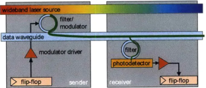
In ATAC the light source, or "optical power supply", is generated by off-chip lasers and coupled into an on-chip waveguide. On-chip light sources exist, but consume large quantities of precious on-chip power and area. The power consumption of an off-chip laser is roughly 1.5 W, with 0.2 W of optical power ending up in the on-chip waveguide.
Waveguides are the on-chip channels for light transmission. They guide and confine light by a combination of a high-refractive--index material on the inside of the waveguide and a low-refractive-index material on the outside (the cladding). Waveguides can be made out of either silicon (Si) or polymer. Due to the fact that Si waveguides can be packed onto
Figure 2-1: Optical transmission of a single bit
a chip at much higher densities and that modulators for Si can be made much more com-pactly, the ATAC design employs Si waveguides. These waveguides can be manufactured in a standard CMOS process, as both the waveguide and cladding materials are commonly used elsewhere. ATAC requires waveguides with losses of less than 0.3dB/cm and total power capacity of about 10 mW, both of which are achievable with Si.
The optical filter is a ring resonator that couples only a specific wavelength from the power supply waveguide to the data waveguide. The exact wavelength, as well as the spacing between wavelengths, is determined by the ring resonator dimensions and is fixed during manufacturing. Limited tuning can be achieved by changing the ring's temperature or by injecting charge into the ring. The modulator is an optical device that imprints a digital signal on the light extracted by the filter by varying the absorption in the device. Modulators are used to translate an electrical signal (amplified by the modulator driver) into an optical signal, and can therefore be thought of as an "optical switch", placing values onto optical waveguides. The modulators are Ge based electro-absorption modulators with integrated filters. The ring resonators are not used for modulation but just for wavelength filtering. It is assumed that athermal design [33] is implemented, so that the rings do not need to be tuned. The modulators used in the ATAC design have characteristics that are expected to be reached by designs available in 2012: insertion loss of 1dB; area less than
50 pm2; modulation rate of 1 Gbps; energy required to switch less than 25 fJ; and power
consumption of 25 pW at 1 GHz [16].
At the receiving end of a waveguide, additional components are used to receive the signal and convert it to an electrical signal. An additional optical filter is used to extract
light of a particular wavelength from the data waveguide and transfer it to a photodetector. The filter can be designed to extract any fraction of the total signal by adjusting the size of the gap between the waveguide and the filter. The photodetector is an extremely sensitive optical device which absorbs photons and outputs an electrical signal. The photodetector proposed for ATAC has a responsivity of greater than 1 Amp/Watt and 3dB bandwidth performance at 1 GHz. It has an area footprint of less than 20 pm2. Furthermore, the
ex-pected capacitance of the photodetector is less than 1 fF [8]. In current technology nodes, the output of the photodetector would need to be amplified by a power-hungry TIA (tran-simpedance amplifier) before it could be used to drive a digital circuit. However, starting with the 22nm node, the smaller transistor input capacitances will allow the photodetector to directly drive a digital circuit, greatly reducing power consumption.
Figure 2-1 puts all of these elements together, showing how one bit is transmitted from a flip-flop of one core to a flip-flop of another core. In this figure, the core on the left shows the components relevant to sending and the core on the right shows the components relevant to receiving; however, in the actual chip all cores would contain both sets of components. From end to end, the process for sending a bit on the ATAC's optical network is as follows. The flip-flop signals the modulator driver to send either a 0 or a 1. The modulator driver, which consists of a series of inverter stages, drives the modulator's capacitive load. The modulator couples light at its pre-tuned wavelength Ai from the optical power source and encodes either a 0 or 1 onto the data waveguide. The optically-encoded data signal traverses the waveguide at approximately one-third the speed of light and is detected by a filter that is also tuned to wavelength Ai. Photons are detected by the photodetector and received by a flip-flop on the receiver side.
Chapter 3
Architecture Overview
As previously illustrated in Figure 1-1, the ATAC processor uses a tiled multicore archi-tecture combining the best of current scalable electrical interconnects with cutting-edge on-chip optical communication networks. The ATAC architecture is targeted at 1000-core chips implemented in a 16nm process. However, it can also be scaled down to smaller chips. In this thesis we describe and evaluate 64- and 1024-core versions. We first review the baseline electrical architecture, and then describe how it is augmented with the optical interconnect.
The underlying electrical architecture consists of a 2-D array of processing cores con-nected by a point-to-point, packet-switched mesh network (called the EMesh) like those seen in other multicore processors [25, 14, 12]. Each core in ATAC contains a single- or dual-issue, in-order RISC pipeline with data and instruction caches (Figure 1-1(c)). ATAC uses a novel directory-based cache coherence scheme with a portion of the directory in each core (see Chapter 4).
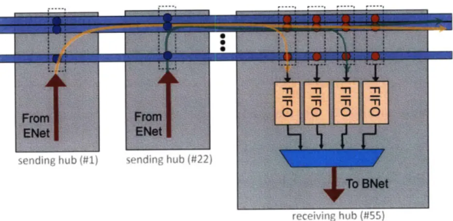
To this electrical baseline, we add a global optical interconnect-the ANet-based on state-of-the-art optical technology. Whereas the EMesh is ideal for predictable, short-range point-to-point communication, the ANet provides low-latency, energy-efficient global and long-distance communication. The key component of the ANet is the all-optical ONet shown in Figure 1-1(a). In the 1024-core ATAC architecture (called ANet'024), cores are grouped into 64 "clusters", each containing 16 cores. Each cluster contains a single ONet endpoint called a Hub. The Hub is responsible for interfacing between the optical
compo-nents of the ONet and the electrical compocompo-nents within a cluster. The ATAC architecture can be scaled down by reducing the number of cores with each cluster. A 64-core chip (called ANet64) would connect each core directly to a Hub.
In ANet10 2 4, individual cores are connected to the Hub in two ways: data going from
a core to the Hub uses the standard EMesh (described above); data going from the Hub to the cores uses the BNet, a small electrical broadcast network (Figure 1-1(b)). In the 22nm node, the clusters are small enough that a flit can travel from the Hub to all cores in a cluster within one clock cycle. Because the BNet is dedicated to broadcasts, it is essentially a fanout tree and requires no routers, crossbars, or internal buffering. It requires only a small amount of buffering and arbitration at the Hub and receiving buffers at the leaves. We estimate that a BNet requires less than one-eighth the area of a full EMesh of the same bitwidth.
The ANet1024 uses a 128-bit wide ONet (128 optical waveguides for data); one 128-bit wide electrical EMesh; and two parallel 128-bit wide BNets. The Hub arbitrates between the two BNets using a static policy: packets sent from clusters with even number IDs on the first BNet and odd number IDs on the second BNet. Together, the ONet, EMesh and
BNet form the complete ANeto24.
3.1
ONet Optical Network
The key to efficient global communication in a large ATAC chip is the optical ONet. The ONet provides a low-latency, contention-free connection between a set of optical endpoints called Hubs. Hubs are interconnected via waveguides that visit every Hub and loop around on themselves to form continuous rings (Figure 1-1(a)). Each Hub can place data onto the waveguides using an optical modulator and receive data from the other Hubs using optical filters and photodetectors. Because the data waveguides form a loop, a signal sent from any Hub will quickly reach all of the other Hubs. Each Hub's filters are tuned to extract approximately 1/64th of the signal, allowing the rest to pass on to the downstream Hubs. Thus every transmission on the ONet is actually a fast, efficient broadcast.
Each Hub has modulators tuned to a unique wavelength to use when sending and contains filters that allow it to receive signals on all of the other wavelengths. This eliminates the need for arbitration in the optical network. Taken together, these features mean that the ONet is functionally similar to a broadcast bus, but without any bus contention.
WDM is a key differentiator of the ATAC architecture from a performance scalability perspective. WDM allows a single waveguide to simultaneously carry bits of many overlap-ping communications. To contrast, an electrical wire typically carries a single bit. Whereas
ATAC may share a single waveguide medium between a large number of simultaneous
communication channels, implementing multiple simultaneous communication channels in the electrical domain requires additional physical wires. For network operations that are expensive to implement in the electrical domain (such as broadcast), the ATAC approach greatly improves efficiency.
The broadcast mechanism of the ATAC architecture is another key differentiator. Opti-cal technology provides a way to build fast, efficient broadcast networks whereas electriOpti-cal mechanisms do not. When using optical components instead of electrical components, signals may travel farther and be tapped into by more receivers before they need be regen-erated. With electrical components, regeneration is accomplished via buffers or sizing-up of transistors for increased drive strength. When these electrical mechanisms are exten-sively employed, as they would be in a large electrical broadcast network, it leads to high energy consumption and poor scaling.
Besides broadcasts, optical technology also allows efficient long-distance point-to-point communication. Initiating an optical signal (i.e., switching the modulator) requires more energy than switching a short electrical wire. However, once generated, the optical signal can quickly travel anywhere on the chip without the need for repeaters. To avoid wasting power and resources delivering these unicast messages to all cores, ATAC includes filtering at the receiving Hubs and cores. Packets labeled as intended for a single core are only rebroadcast on the BNet of the cluster containing that core. In addition, the other cores in
that cluster will drop the packet immediately, rather than processing it.
The ATAC architecture was carefully designed taking into account the physical limi-tations and constraints of both the optical (see Chapter 2) and electronic devices. Based
Figure 3-1: Hub-to-hub communication over the ONet
on these constraints, the ONet as described above should scale to at least 64 (and
possi-bly as many as 100) Hubs. This limit is based on several factors: 1) the total range of
wavelengths over which the optical devices can be tuned divided by the minimum spacing between wavelengths, 2) the total amount of optical power a waveguide can carry divided
by the minimum amount that each photodetector needs to receive to reliably register a
signal, and 3) the maximum length of a waveguide based on the acceptable propagation losses.
These limits can be overcome using multiple waveguides and dividing the communica-tion channels between them. However, eventually the area needed for the optical compo-nents will become the limiting factor. The ONet's optical compocompo-nents and photonic inter-connect can be placed on a separate layer in the CMOS stack, and can therefore overlap the
electrical components to which they connect. However, for a 400 mm2 chip, the entire area
would be consumed by an ONet with approximately 384 Hubs. Since we believe that chips will eventually grow to thousands of cores, some sharing of Hubs will certainly be needed. Therefore, for the purposes of this thesis, we take the simple approach and assume that the ONet is limited to 64 Hubs.
Sending data using the ONet is shown in more detail in Figure 3-1. To provide adequate on-chip bandwidth, the ONet uses a bundle of waveguides, each waveguide containing 64 wavelengths. The ONet contains 128 waveguides for data, one for backwards flow con-trol, and several for metadata. The metadata waveguides are used to indicate a message
type (e.g., memory read, barrier, raw data) or a message tag (for disambiguating multiple messages from the same sender). ATAC, thus uses multiple waveguides to increase the bandwidth of its optical network (ONet) and keeps the network operating frequency at the frequency of the core (1 GHz). Hence, ATAC does not require any sophisticated clock synchronization schemes for the optical network. Each of the 64 Hubs transmits data on its unique wavelength without interference. Figure 3-1 shows two Hubs sending their data simultaneously without interference. The receiving Hub captures both of the values simul-taneously into sender-Hub-specific FIFOs. These values are then propagated to the cores using the BNet.
3.2 Cache Subsystem
The data caches across all cores on the ATAC chip are kept coherent using a directory-based coherence protocol called ACKwise described in more detail in Chapter 4. The directory is distributed evenly across the cores. The directory in each core is stored in SRAM memory and is organized as a directory cache. Furthermore, each core is the "home" for a set of
addresses (the allocation policy of addresses to homes is statically defined).
3.3 External Memory Subsystem
When cores need to communicate with external memory, they do so via several on-chip memory controllers. Each cluster has one core replaced by a memory controller. After receiving requests through the ANet, the memory controller communicates with external DRAM modules through 1/0 pins. Replies are then sent back to the processing cores through the ANet. Other ATAC chips with different memory bandwidths are possible by varying the number of cores replaced by memory controllers.
The primary task of the memory controller is to translate requests from the process-ing cores into transactions on a memory I/O bus. The choice of 1/0 bus technology is independent of the on-chip network architecture since the memory controller is performing a translation. However, to support the large number of memory controllers needed for a
1000-core chip, we assume that the connection to memory is optical as well.
A detailed design for an optical memory subsystem is left to future work. However, we
can assume that an optical memory bus would consist of some number of on-chip waveg-uides that are coupled to external fibers, effectively creating optical "pins." Each optical pin could carry up to 64 wavelengths of light at speeds of up to 20 GHz. The actual trans-mission speed would likely be limited by design trade-offs in the electrical circuits driving the optical components. We estimate that optical 1/0 pins operating at 5 GHz (yielding 40 GB/s of bandwidth) should be practical. Thus each off-chip memory bus can be imple-mented using a single optical pin. This makes it practical to integrate the large number of memory controllers needed to meet the bandwidth needs of future 1000-core chips.
Chapter 4
Cache Coherence Protocol
This chapter presents ACKwise [13], a novel cache coherence protocol derived from a MOESI-directory based protocol [28]. Each directory entry in this protocol, as shown
in Figure 4-1 is similar to one used in a limited directory scheme [2] but with a few modi-fications. The 3 fields in each directory entry are as follows: (1) State: This field specifies the state of the cached block(s) associated with this directory entry (one of the MOESI states); (2) Global(G): This field states whether the number of sharers for the cache block exceeds the capacity of the sharer list. If so, a broadcast is needed to invalidate all the cached blocks corresponding to this address when a cache demands exclusive ownership;
(3) Shareri -Sharerk: These fields represent the sharer list. The ACKwise protocol which
holds the identities of a maximum of k sharers is denoted as ACKwisek.
When the number of sharers exceeds k, the global(G) bit is set so that any number of sharers beyond this point can be accommodated. Once the global(G) bit is set, the Sharerk field holds the total number of sharers. The Shareri -Sharerk_1 fields still hold the identity
of k - 1 distinct sharers.
State 4 G1 Shrctre o ws diet -a r enrk
4.1 Operation of the ACKwisek Protocol
When a request for a shared copy of a cache block is issued, the directory controller first checks the state of the cache block in the directory cache. (a) If the state is Invalid(I), it forwards the request to the memory controller. The memory controller fetches the cache block from memory and sends it directly to the requester. It also sends an acknowledgement to the directory. The directory changes the state of the cache block to Exclusive(E) and sets
the Sharer1 field to the ID of the requester. (b) If the state is one of the valid states (i.e.,
one of MOES), it forwards the request to one of the sharers. The sharer forwards the cache block directly to the requester and sends an acknowledgement to the directory. Appropriate state changes happen in the directory according to the rules of the MOESI protocol [28]. The directory controller also tries to add the ID of the requester to the sharer list. This is straightforward if the global(G) bit is clear and the sharer list has vacant spots. If global(G) bit is clear but the sharer list is full, it sets the global(G) bit and stores the total number of
sharers (in this case, k + 1) in the Sharerk field. If the global(G) bit is already set, then it increments the number of sharers by one.
When a request for an exclusive copy of a cache block is issued, the directory controller first checks the state of the cache block in the directory cache. (a) If the state is Invalid(I), the sequence of actions followed is the same as that above except that the state of the cache block in the directory is set to Modified(M) instead of Exclusive(E). (b) If the state is one of the valid states (i.e., one of MOES), then the directory controller performs the following 2 actions: (i) It forwards the request to one of the sharers. (ii) If the global bit is clear, it sends unicast invalidation messages to each core in the sharer list. Else, if the global bit is set, it broadcasts an invalidation message (to all the cores in the system). Now, the sharer which receives the forwarded request sends the cache block directly to the requester, invalidates the block and acknowledges the directory. The other sharers invalidate their cache blocks and acknowledge the directory. The directory controller expects as many ac-knowledgements as the number of sharers (encoded in the Sharerk field if the global(G) bit is set and calculated directly if the global(G) bit is clear). After all the acknowledge-ments are received, the directory controller sets the state of the cache block to Modified(M),
the global(G) bit to 0 and the Sharer1 field to the ID of the requester. Due to the
broad-cast capabilities of ATAC as described in Chapter 3, the sending of broadbroad-cast messages can be achieved easily. In addition, the ACKwisek protocol requires only as many uni-cast acknowledgements as a full-map directory-based protocol. Hence the name ACKwise since the protocol intelligently tracks the number of sharers of a cache block and requires acknowledgements from only the actual sharers on an invalidation broadcast message.
4.2 Silent Evictions
Silent evictions refer to the evictions of clean shared data from the cache of a core with-out notifying the directory that the core is no longer a sharer of the data. Silent evictions are supported in certain cache coherence protocols since they are found to increase sys-tem throughput by decreasing network utilization. Silent evictions are not supported in the ACKwise protocol since the directory should always have an accurate count of the number of sharers of a cache line for correct operation. However, our measurements show that disallowing silent evictions is not detrimental to the performance of the ACKwise proto-col because: (1) the additional coherence messages do not lie on the critical path of load or store misses and hence do not directly affect the average memory latency and thereby processor performance; (2) these messages do not include data and hence contribute only a small percentage to the overall network traffic and thereby do not really affect the network latency.
Chapter
5
Power Modeling
This chapter discusses the power estimation techniques used to compare the ATAC network (ANet) against an electrical mesh network (EMesh). Section 5.1 talks about the power esti-mation techniques used for the electrical mesh network while section 5.2 details the power estimation techniques for the ATAC network, showing how aggressive and conservative optical technology predictions affect the energy consumption of its constituent optical net-work.
5.1 Electrical Mesh Network
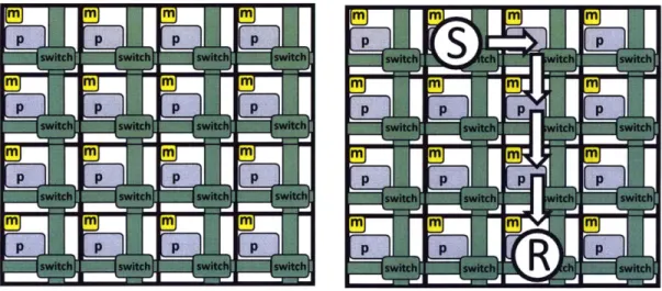
The electrical mesh is composed of routers and links arranged in a mesh topology as shown in Figure 5-1. Communication between tile A and tile B is realized using multiple hops as shown in Figure 5-2. (Here, communication between tile A and tile B takes 4 hops). During each hop, the packet is processed by a router and traverses a link.
The packet processing stages of a router are as follows:
1. Buffer Write (if the downstream link is contended)
2. Switch Allocation
3. Buffer Read (if the downstream link is contended)
Figure 5-1: Electrical Mesh Network con- Figure 5-2: Routing of a Packet between
necting 16 tiles tile A and tile B
The buffer write and read stages only occur if the downstream link is contended. The different components of a router, including the buffer, the switch allocator and the crossbar are shown in Figure 5-3. Static power and dynamic energy for the four processing stages of the router as well as for the link are computed using Orion [5]. Event counters are main-tained during simulation that increment whenever an activity occurs (such as link traversal, buffer write, etc.) and at the end of simulation, the events counters are multiplied by the dynamic energy associated with each event (obtained from Orion citeorion) to get the total dynamic energy. Total static energy is computed by summing the static power associated with each component of the network and multiplying that number by the total simulation time. Static power and dynamic energy estimates for the router and link components of a 256-bit wide electrical mesh are shown in Table 5.1. Dynamic energy estimates are for a
1-flit (256-bit) packet assuming half the bits flip.
Electrical Mesh Component Dynamic Energy Static Power
Buffer (Read + Write) 22.05 pJ 21.98 mW
256-bit 5 x 5 Router Crossbar 59.34 pJ 32.32 mW
Switch Allocator 0.44 pJ 0.41 mW
256-bit Link Link 18 pJ 9.4 mW
Table 5.1: 256-bit wide Electrical Mesh Energy Parameters
E E
Input Otu
Por ---Port + Crossba s Output
Ports
P P
Buffer Bypass Path
Figure 5-3: Electrical Mesh Router Microarchitecture
Energy/bit Calculation The average dynamic energy consumption per bit in an electrical
mesh is given by the following equation:
Average Dynamic Energy per bit
Dynamic Energy per Packet per Hop x Average Number of Hops Packet Size x Flit Size
2VW x (B x (DynamicBuffer + Dynamiccrossbar + DynamicLink) + DynamicsA)
3xBxW
The average number of hops of a packet in an N-tile (vW x vW) electrical mesh
network is . In the above equation, B(= 2) stands for the average number of flits in a
packet; W(= 256) stands for the number of bits in a flit; N(= 1024) is the number of cores; and Dynamiccomponent is the dynamic energy associated with each network router or link component. Dynamic energy values are substituted from Table 5.1. Average dynamic energy per bit is computed to be 8.3 pJ (6.8 pJ from router and 1.5 pJ from link). If the packet traverses only k hops, the average dynamic energy per bit is 390 x k fJ. The results are summarized in Table 5.2.
Modeling Inaccuracies All electrical network power estimates are obtained at 32 nm
from Orion even though 1024 cores cannot be fabricated on a chip until the 22 nm technol-ogy node. Moreover, Orion's models are calibrated at 65 nm and then scaling factors are
Table 5.2: Dynamic Energy per bit on a 256-bit wide Electrical Mesh Network.
applied to get power estimates at 32 nm.
5.2
ATAC Network
The building blocks of the ATAC network (ANet) include a modified electrical mesh net-work, an all-optical network (ONet) and a broadcast network (BNet). Denote the modified
electrical mesh network as ENet for this discussion. There is one ENet, one ONet and C x 2
BNets' in the ATAC network (C being the number of clusters). The topology of the ATAC
network is shown in Figure 5-4.
II
I
L I
1
ONet
(a) 64 Optically-Connected Clusters
ANet = ONet + BNet + EMesh BNet
\EMesh
(c) core architecture
(b) Electrical In-Hub Networks
Connecting 16 Cores
Figure 5-4: ATAC Network Architecture
5.2.1 ENet
The ENet can be modeled as an electrical mesh where two routers is each cluster have an additional output port to connect to the Hub. Since the bandwidth bottleneck is at the Hub and not in the ENet, this will suffice. (The ENet can sustain a throughput of 256 bits/cycle
L
1
IF-jr-1
to the Hub while the Hub can only process 128 bits/cycle). Dimension-order (X-Y) routing is followed to send packets from a tile to the Hub.
ENet Component Dynamic Energy Static Power
Buffer (Read + Write) 11.07 pJ 11.18 mW
128-bit 5 x 5 Router Crossbar 21.21 pJ 16.22 mW
Switch Allocator 0.44 pJ 0.41 mW
128-bit Link Link
j9
pJ 4.7 mWTable 5.3: 128-bit wide ENet (Modified Electrical Mesh) Energy Parameters
5.2.2
ONet
Optical Losses Aggressive
[Conservative
Waveguide Propagation Loss 2 dB (0.2 dB/cm) 10 dB (1 dB/cm)
Modulator Insertion Loss 1 dB 3 dB
Filter Set Through Loss le-2 dB 1 dB
Filter Drop Loss 1 dB 2 dB
Backplane Coupler Loss 1 dB 2 dB
Splitter Loss 1 dB 1 dB
Photodetector Loss 0.1 dB 1 dB
Total 7 dB 20 dB
Table 5.4: Optical Waveguide Losses
The optical network is composed of an off-chip laser source that produces photons, waveguides for the transmission of photons, modulators for imprinting a digital signal on the wavelengths and a photodetector for receiving the data. Refer to Chapter 2 for more details on the optical background. The power consumption of the all-optical ONet can be calculated by adding the static power of the laser and the rings and the dynamic power
Laser Power (per wavelength) Aggressive Conservative
Charge required to flip gate (Qg) 1.88 fC 4.28 fC
Optical Losses 7 dB 20 dB
Frequency (fc) 1 GHz 1 GHz
Responsivity of Photodetector (Rd) 1.1 A/W 1.1 A/W
Number of Detectors (NR) 64 64
Laser Power (per wavelength) 0.55 mW 29.4 mW
Power Component Aggressive Conservative
Sender Dynamic Energy (Modulator + Modulator Driver) 10 fJ 45 fJ
Receiver Dynamic Energy (Photodetector + Receiver) 2.3 fJ 15 fJ
Laser Power (per wavelength) 0.55 mW 29.4 mW
Ring Tuning Power (per ring resonator) 0 mW 0.02 mW
Table 5.6: ONet Power Components
of the modulator, modulator driver, photodetector and photodetector receiver. The ONet power components are listed in Table 5.6.
Laser Power
The total laser power is dependent on the following five factors:
1. Optical Losses (L)
2. Operating Frequency (fc)
3. Number of Receivers (NR)
4. Responsivity of Photodetector (Rd)
5. Laser efficiency (E)
To calculate the optical laser power, first all the optical losses are enumerated. This is done in Table 5.4. Next, the capacitance of the receiver is calculated by summing the capacitance of the photodetector, the wire connecting the photodetector and the transistor and the gate capacitance of the transistor. At 11 nm, this capacitance is aggressively and conservatively estimated to be 2.35 fF and 5.35 fF respectively. With an operating voltage of 0.8 V, the aggressive and conservative estimates for the charge needed to flip a gate,
Q
9 are 1.88 fCand 4.28 fC respectively. The operating frequency,
fc
is I GHz and the number of receiversper wavelength, NR is 64. The responsivity of the photodetector, Rd is 1.1 A/W. The
amount of optical laser power per wavelength per bit is given by the following equation.
Poptical =10 XQgxfcxNR (5.1)
The electrical laser power per wavelength per bit is given by the following equation.
Pelectrical Poptical (5.2)
The above calculations for computing laser power are shown in Table 5.5.
Ring Ining Power
An athermal design of ring resonators has been proposed in [33]. However it is not clear whether such designs are easy to be built and are compatible with a monolithic silicon fabrication process. Hence, a ring tuning power of 0 mW is used as an aggressive estimate. The conservative estimate is calculated by assuming a ring tuning power of 1 pW for a 1 K temperature range. Assuming a normal operating temperature range of 20 K, this comes out to be 0.02 mW per ring resonator.
Modulator + Modulator Driver Power
Based on aggressive and conservative predictions of the capacitance of the devices, the dynamic energy is estimated to be 10 fJ and 45 fJ respectively.
Photodetector + Receiver Power
Based on aggressive and conservative projections of the capacitance of the devices, the dynamic energy is estimated to be 2.3 fJ and 15 fJ respectively.
5.2.3
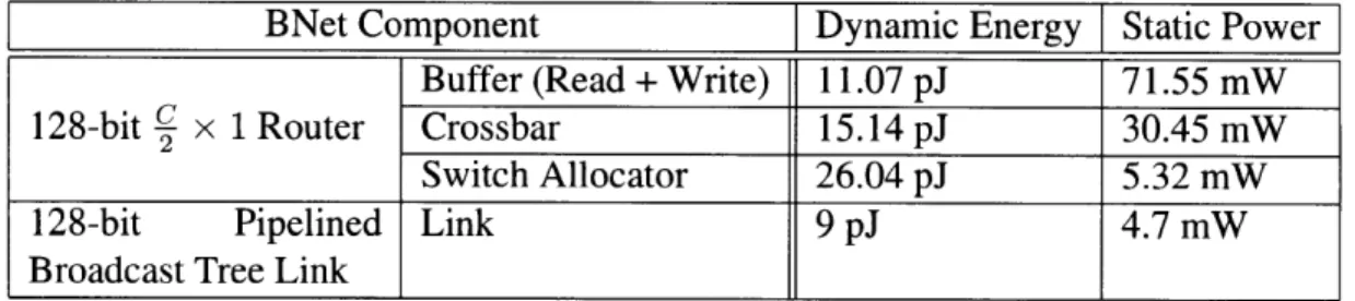
BNet
The BNet connects the Hubs to the cores as discussed in Chapter 3. Since there are only 2 BNets per cluster, the data that arrives on the ONet compete for access to the BNet. The data that arrives from the different clusters is statically partitioned among the BNets according to the sender cluster's ID. A BNet is composed of the following two elements.
1. A ! x 1 router (2 inputs and 1 output) that arbitrates between the data received from2 c
2. A pipelined broadcast bus that transports data from the output port of the router to all the tiles in the cluster.
The C x 1 router is modeled using Orion [5]. The dynamic energies due to the buffers, switch allocators and crossbar are faithfully modeled. The pipelined broadcast bus is mod-eled as a tree of links that connect the Hub to all the tiles in the cluster. There are n + 1 nodes in this tree (n tiles + 1 Hub). Hence, the tree is composed of n electrical links and the length of each electrical link is equal to the width of a tile. Each electrical link is again modeled using Orion [5].
BNet Component Dynamic Energy Static Power
Buffer (Read + Write) 11.07 pJ 71.55 mW
128-bit 2 x 1 Router Crossbar 15.14 pJ 30.45 mW
Switch Allocator 26.04 pJ 5.32 mW
128-bit Pipelined Link 9 pJ 4.7 mW
Broadcast Tree Link
Table 5.7: 128-bit wide BNet (Pipelined Broadcast Tree) Energy Parameters. C stands for the number of clusters (C = 64). n stands for the number of tiles in each cluster (n = 16).
Energy/bit Calculation To calculate energy/bit, the contributions of the three constituent
networks (ENet, ONet and BNet) are considered.
For the ONet network, the average dynamic energy per bit is given by the following equation:
Average Dynamic Energy per bit(ONet)
= Dynamic Energy of Modulator + C x Dynamic Energy of Receiver
For the ONet network, the average static energy per bit is given by the following equa-tion:
Average Static Energy per bit(ONet)
Laser Power (per wavelength per bit)
+
C x Ring Tuning PowerANet Component Dynamic Energy (per bit) Static Energy (per bit)
ONet 157 fJ 550 fJ
ENet 480 fJ
-BNet 1533 fJ
Total 2.72 pJ
Table 5.8: Energy/bit computation for the ANet network assuming aggressive optical
tech-nology predictions.
For the ENet and BNet networks, the average dynamic energy per bit is calculated as illustrated in Section 5.1. The results are summarized in Table 5.8.
Here, 2.72 pJ is the average energy consumed to transmit a bit on the 128-bit wide ANet. 390 fJ is the energy required to transmit a bit across one hop in a 256-bit wide EMesh (see Table 5.2). Hence, transmitting a bit between two cores that are at least 7 hops apart is more energy-efficient on the ANet network.
Chapter 6
Evaluation
The purpose of this section is to: (1) Demonstrate the capabilities of the ATAC network
(ANet) over a pure electrical mesh network (EMesh), (2) Demonstrate the performance
advantages of using the ACKwisek protocol over the DirkB and DirkNB limited directory-based cache coherence protocols [2], and (3) Perform an energy comparison of the ATAC network assuming both aggressive and conservative optical technology predictions with an electrical mesh network.
DirkB is a limited directory based protocol which broadcasts once the capacity of the
sharer list is exceeded and collects acknowledgements from all the cores in the system.
ACKwisek on the other hand, intelligently tracks the number of sharers once the capacity
of the sharer list is exceeded and needs acknowledgements from only the actual sharers of the data on a broadcasted invalidation. Dir NB always ensures that the number of sharers of a cache line is less than the capacity of the sharer list. k denotes the number of hardware sharers in each of the above protocols. This section evaluates the performance of Splash2 and Parsec benchmarks as well as synthetic applications on 64 and 1024 cores using six combinations of on-chip networks and cache coherence protocols: (a) ANet-ACKwisek,
(b) ANet-DirkB, (c) ANet-DirkNB, (d) ACKwisek, (e) DirkB and (f) EMesh-DirkNB. Results demonstrate the advantages of using ANet over EMesh due to its higher
bandwidth, lower latency and broadcast capabilities as well as the performance benefits of the ACKwisek protocol over the DirkB and DirkNB protocols.
Core Model In-Order
Frequency 1 GHz
EMesh Hop Latency 2 cycles(router delay - 1, link traversal - 1)
ONet Hop Latency 3 cycles(E/O + O/E conversion - 2, link traversal - 1)
1024 cores
ANet10 2 4 = ONet + ENet + 64x2 BNets
ONet 128-bit wide
ENet 128-bit wide
BNet 128-bit wide
EMesh for comparison 256-bit wide
Memory Bandwidth 64 memory controllers
5 GBps per controller
L2 Cache Size 32 KB
64 cores
ANet64 = ONet + ENet
ONet 64-bit wide
ENet 32-bit wide
EMesh for comparison 64-bit wide
Memory Bandwidth 4 memory controllers
5 GBps per controller
L2 Cache Size 256 KB
Table 6.1: Target System Architecture Configuration Parameters
6.1 Methodology
The Graphite [20] distributed multicore simulator is used for all evaluations in this section. For the 64 core simulations, the ANet64 network is compared to a 64-bit wide electrical
mesh network. For the 1024 core simulations, the ANet1024 network is compared to a
256-bit wide electrical mesh network. The above comparisons are justified because the optical components of the ONet can be placed on a separate layer, thereby making the ONet have only few area requirements for receiver-side electrical buffering and arbitration. In addition, the area of a 128-bit wide BNet is roughly one-eighth the area of a 128-bit wide electrical mesh (see Chapter 3).
Table 6.1 summarizes the detailed target architectures. In ANet64, short unicast
mes-sages less than four hops away are sent on the EMesh while broadcasts and long unicast
the EMesh network while inter-cluster communication is carried out using the ENet, ONet and BNet networks. Small private L2 cache sizes were assumed for the 64-core study due to the small working set sizes of Splash2 benchmarks. All the references to EMesh in the remaining part of the evaluation section refer to the respective 64-core 64-bit wide
and 1024-core 256-bit wide pure electrical mesh networks against which the ANet64 and
ANet1 024 networks are compared.
6.2 Performance Evaluation
6.2.1
Parsec and Splash2 Benchmarks
Nine applications from the Splash2 benchmark suite and three applications from the Parsec benchmark suite are simulated on 64 and 1024 cores using the 6 combinations of cache coherence protocols and networks mentioned previously.
64 cores
The configurations ANet-Dir64NB and ANet-Dir64B are expected to show the same
perfor-mance as ANet-ACKwise64 since the directory type of the cache coherence protocol does not
play a role when the number of hardware sharers is equal to the number of cores simulated.
Similarly, the performance of EMesh-ACKwise64, EMesh-Dir64NB and EMesh-Dir64B are
expected to be the same. In the following discussion, ANet refers to ANet64 described in
Table 6.1.
Figure 6-1 plots the performance of the twelve benchmarks observed when running with the DirkNB cache coherence protocol on the ANet and EMesh networks. The perfor-mance is plotted as a function of the number of hardware sharers (k). Results are
normal-ized to the performance observed when running with EMesh-Dir2NB. With the DirkNB
protocol, ANet is observed to outperform EMesh at all values of k and the performance difference is observed to decrease with increasing values of k. ANet-Dir2NB outperforms
EMesh-Dir2NB by 30.9% while ANet-Dir64NB outperforms EMesh-Dir64NB by 12.8%.
Dir(k)NB Performance: ANet and EMesh 64 cores S8 96_ k=2 Z 4 - - -k=4 3 - Ek=8 0 2 1 Ek=16 W *k=32 ."S 4 Ek=64 1.8 _ z 1.6 1.4 k= 2 9 1.2 -- ---~ *k=3 2 0.8-0.6 - 6 Mk=16 0 *k=32
Figure 6-1: Performance of Splash2 and Parsec benchmarks when using the DirkNIB pro-tocol on the ANet and EMesh networks. Results are normalized to the performance of EMesh-Dir2NB. The number of hardware sharers are varied as 2, 3, 4, 8, 16, 32 and 64. The x-axis values take the form benchmark - network. A and E stand for ANet and EMesh networks respectively.
of hardware sharers. The performance is extremely poor at low numbers of sharers and gradually improves as the number of sharers is increased. On the ANet network, Dir64NB outperforms Dir2NB by an average of 2.63x and a maximum of 5.51x (in water-spatial). On the EMesh network, Dir64NB outperforms Dir2NB by an average of 3.04x and a maxi-mum of 8.29x (also in water-spatial).
The above results can be understood by observing Figure 6-4 which plots the cache miss rates of the benchmarks when run with the DirkNB protocol. The cache miss rates are observed to decrease as the number of hardware sharers (k) is increased. Hence, the performance increases with an increase in the value of k. High cache miss rates occur at low values of k due to the presence of a large number of true shared reads in these benchmarks.
(A core is said to perform a true shared read when it reads from an address that is cached by
Dir(k)B Performance: ANet and EMesh 64 cores 9 8 f 7 k = 3 %A *k=32 U 4 - - - --- k= 4 3 -~Mk=8 'ii M, k 1
Figure 6-2: Performance of Splash2 and Parsec benchmarks when using the DirkB protocol on the ANet and EMesh networks. Results are normalized to the performance of EMesh-Dir2NB. The number of hardware sharers are varied as 2, 3, 4, 8, 16, 32 and 64. The x-axis
values take the form benchmark -network. A and E stand for ANet and EMesh networks
respectively.
ACKwise(k) Performance: ANet and EMesh 64 cores 2 8 k=2 6 5_ _ _ _ __ _ _ _ __ _ k=3 CO2 'k= 16 0 *k=32 U. or4
4>
C3?_ k~ =64Figure 6-3: Performance of Splash2 and Parsec benchmarks when using the ACKwisek protocol on the ANet and EMesh networks. Results are normalized to the performance of EMesh-Dir2NB. The number of hardware sharers are varied as 2, 3, 4, 8, 16, 32 and 64.
The x-axis values take the form benchmark -network. A and E stand for ANet and EMesh
networks respectively.
invalidations because a large number of cores try to simultaneously read globally shared data and evict each others' cache lines in the process due to the restriction on the number of hardware sharers. The rate of increase of performance with k is directly correlated to the rate of decrease of cache miss rates with k as can be observed from Figures 6-1 and 6-4. This explains why benchmarks like water-spatial show a speedup of 8.29x on EMesh while others like lu.non-contiguous show very little speedup (9% on EMesh) when the number of hardware sharers is increased from 2 to 64. The cache miss rates of all benchmarks except
.