Design of a Low-Voltage Low-Power dc-dc
HF Converter
by
Jingying Hu
B.S., Illinois Institute of Technology (2005)
Submitted to the Department of Electrical Engineering and Computer
Science
in partial fulfillment of the requirements for the degree of
Master of Science
at the
MASSACHUSETTS INSTITUTE OF TECHNOLOGY
February 2008
@ Massachusetts Institute of Technology, MMVIII. All rights
reserved.
Author
Department of Electrical Engineering and
Certified by.
7 /
Computer Science February 1, 2008
David J. Perreault Associate Professor of Electrical Engineering Thesis Supervisor Accepted by. MASSAC8U8WR97WIN$Tfi1e OF TEOHNOLOGY
APR
0 7 2008
LIBRARIES
/ Terry P. OrlandoChairman, Department Committee on Graduate Students
ARRCVES
Design of a Low-Voltage Low-Power dc-dc HF Converter
by
Jingying Hu
Submitted to the Department of Electrical Engineering and Computer Science on February 1, 2008, in partial fulfillment of the
requirements for the degree of Master of Science
Abstract
Many portable electronic applications could benefit from a power converter able to achieve high efficiency across wide input and output voltage ranges at a small size. However, it is difficult for many conventional power converter designs to provide wide operation range while maintaining high efficiency, especially if both up-and-down voltage conversion is to be achieved. Furthermore, the bulk energy storage required at contemporary switching frequencies of a few megahertz and below limits the degree of miniaturization that can be achieved and hampers fast transient response. There-fore, design methods that reduce energy storage requirements and expand efficient
operation range are desirable. This thesis focuses on the development of a High Fre-quency (HF) dc-dc SEPIC converter exploiting resonant switching and gating with fixed frequency control techniques to achieve these goals.
The proposed approach provides high efficiency over very wide input and output volt-age ranges and power levels. It also provides up-and-down conversion, and requires little energy storage which allows for excellent transient response.
The proposed design strategies are discussed in the context of a prototype converter operating over wide input voltage (3.6 - 7.2V), output voltage (3 - 9V) and power (0.3 - 3W) ranges. The 20MHz converter prototype, utilizing commercial vertical MOSFETs, takes advantage of a quasi-resonant SEPIC topology and resonant gat-ing technique to provide good efficiency across the wide operatgat-ing ranges required. The converter efficiency stays above 80% across the entire input voltage range at the nominal output voltage. The closed-loop performance is demonstrated via an imple-mentation of a PWM on-off control scheme, illustrating the salient characteristics in terms of additional control circuitry power dissipation and transient response.
Thesis Supervisor: David J. Perreault
Acknowledgements
First and foremost, I want to thank my thesis advisor, Professor David J. Perreault, for his patience and support throughout the course of this work. I feel extremely blessed to be working under and with such an outstanding engineer, caring advisor and knowledgable individual. I cannot thank him enough for all the extra hours he has spent guiding and assisting me through the course of this project.
My thanks go to the Society of Presidential Fellows at MIT and The Charles Stark Draper Laboratory for sponsorship. To Seth M. Davis, my supervisor at C.S. Draper Laboratory, for providing his valuable time and inputs.
To Juan Rivas and Anthony Sagneri, my knowledgable co-workers, inspiring teachers, and close friends, for their invaluable technical expertise and experience in addition to their constant encouragements. To Grace Cheung, our UROP, for her very much enjoyed company. Thank you all for making the basement laboratory such a pleasant place to work at. I also want to acknowledge the contributions, things I have learned and help I have received from other members of my research group, Yehui Han, Robert Pilawa, David Giuliano, Olivia Leitermann, Brandon Pierquet and Wei Li. I am also grateful for all the assistance the LEES staff has provided.
To Dr. Alexander J. Flueck, Dr. Qing H. Liu and Dr. Loren W. Nolte, for offering their advise, guidance and knowledge throughout my undergraduate years to help me grow as a student and as a person. Without the support and the opportunities they have given me, I would not have been given this chance to study at this institution. To all my friends who have been there for me over the years: Wenting (my closest friend in Shanghai), Chao, Jiang, Rach (my beloved roomie), Gina, Kelly, Sahar, Sushma, Patricia, Devonte, Matt, Nathan, Nick, Justin, Sanj, Richard and Kalvyn. To LP, for always knowing the hottest spots in town, whom I can count on whenever I need a fun night out to relax and recharge. Thank you all for everything! The time that we have shared together will always be a part of my most cherished memories. To Randy, for his selfless friendship during a stressful period when I felt like there was nobody else to turn to. Thanks for being there for me through that difficult phase of my life.
-5-me.
To Rui, my cousin, for being the perfect daughter, setting the standards high, and putting up with me through all these years. To my grandparents, for their balanced encouragement and discipline as I was growing up (in addition for providing a safe haven whenever dad got mad).
I owe my deepest gratitude to my parents, who gave up everything they had in Shanghai(family, friends, career, status, title and reputation) and moved to the US in their late 40s/early 50s so that I can have a place to call home in the US. Thank you for teaching me so much about love, work and life. Without your unconditional love and support, I would be nowhere close to where I am today.
-6-1 Introduction
1.1 Challenges of Increasing Converter Switching Frequency ... 1.2 High Frequency Resonant Power Conversion . ... 1.3 Contributions and Organization of the Thesis ...
2 A Quasi-Resonant SEPIC Converter
2.1 Limitations of conventional SEPIC converters . . . . . 2.1.1 Conventional Hard-switched SEPIC Converters 2.1.2 Multi-Resonant SEPIC converters ... 2.2 A New Quasi-Resonant SEPIC Topology ...
2.2.1 Background . . ... 2.2.2 Converter Design ... 2.2.3 Resonant Rectifier ...
2.2.3.1 Basic Operating Principles ...
2.2.3.2 Rectifier Tuning Procedure . . . . 2.2.4 Matching Network ...
2.2.4.1 Tuning the Matching Network ... 2.2.5 Inverter Design ...
2.2.5.1 Inverter Tuning Procedure ...
2.2.5.2 Other Tuning Considerations . . . . . 2.2.6 Summary . .... ... 27 . . . . . 27 . . . . . 29 .. . . . 30 .. . . . 31 .. . . . . 31 .. . . . 34 .. . . . 35 .. . . . . 36 .. . . . 36 .. . . . . 44 . . . . . 46 .. . . . 47 .. . . . 50 .. . . . 58 .. . . . 70 .. . . . 75 2.3 The Power Stage
-8-2.3.1 Device Selection Considerations . . . . 2.3.2 Converter Design ... ...
2.4 Comparison with other Resonant Topologies . . . .
3 Inductor Design
3.1 Air Core Inductors ... . . . ... 3.1.1 Commercial Air Core Inductors . . . . 3.1.2 Air-cored Solenoid Inductors ...
3.1.3 Multi-layer Air-Cored Toroidal Inductors . 3.2 Planar Spiral Inductor Design . ... .
3.2.1 Hand Calculations . . . .. 3.2.2 Spiral Inductor Implementation ...
4 Resonant Gate Drive
4.1 Hard Gating ... ... 4.2 Resonant Gating ...
4.2.1 A Basic Resonant Gate Drive .. . . . .. ...
4.2.2 Improved Resonant Gate Drive . . . . 4.2.2.1 Tuning the Gate Drive . ...
4.2.2.2 Implementation of a Resonant Gate Drive ... 4.3 Comparison with other Resonant Gate Drive Methods ...
4.3.1 A Simple Self Oscillating Gate Driver . ... 4.3.2 A Multi-Resonant Self-Oscillating Gate Driver ...
5 Control Architecture
5.1 Background . ... 5.2 Burst Mode Control . ...
5.3 PWM On-off Control ... . . ... . .. -9-Contents 75 78 82 87 . . . . . 87 . . . . . . . 88 .. . . . . 88 . . . . . 88 . . . . . 90 . . . . . 90 . . . . . 94 96 96 98 98 99 101 103 106 106 108 111 111 112 112
5.3.1 Implementation ... ... ... 113
5.3.2 Comparison with Hysteretic On-off Control ... 116
6 Converter Prototype 118 6.1 Prototype Layout ... ... ... 118
6.2 Impedance Characterization ... .... 119
6.3 Experimental Results ... ... 127
6.3.1 Open Loop Performance ... .. 127
6.3.2 Closed Loop Performance ... . 129
7 Conclusion 139 7.1 Thesis Summary ... ... 139
7.2 Thesis Conclusions ... ... 140
7.3 Future Work ... . ... 141
A SPICE DECKS AND COMPONENT VALUES 145 A.1 Chapter 2 Data ... ... ... 145
A.1.1 Conventional and Multi-Resonant SEPIC data: . ... 145
A.1.2 Rectifier data: ... .... ... 152
A.1.3 Inverter data: ... ... 156
A.1.4 Converter data: . ... ... 183
A.1.5 Other Topologies data: . ... . . . . . 189
A.2 Chapter 4 Data ... .... ... 203
A.2.1 Sinusoidal Resonant Gate Drive data: . ... 203
A.2.2 Self-Oscillating Gate Drive data: . ... 207
A.2.3 SPICE Model Libraries ... ... 213
B PCB Layout Masks and Schematics 222
-Contents
1.1 Class E Inverter ... ... . 23
2.1 Conventional SEPIC Converter ... . . 28
2.2 Efficiency of Conventional SEPIC Converter . ... 30
2.3 Multi-Resonant SEPIC ... ... 32
2.4 Multi-Resonant SEPIC Converter Operation at Different Output Volt-ages ... ... 33
2.5 Resonant SEPIC topology ... ... 34
2.6 Resonant Rectifier Topologies ... ... 35
2.7 Rectifier Waveforms ... ... 37
2.8 Fundamentals of Rectifier Voltage and Current Waveforms ... 38
2.9 Resonant Rectifier Performance as LRECT Varies ... . 39
2.10 Resonant Rectifier Tuned Inductively vs. Capacitively ... 40
2.11 Rectifier Performance with Two Diodes . ... 41
2.12 Rectifier Waveforms as Fc and Zo varies . ... 42
2.13 Rectifier Phase ... ... . 43
2.14 Matching Network Configurations ... . 44
2.15 Matching Network Impedance ... ... 45
2.16 Inverter Topology ... ... 48
2.17 Inverter with Matching Network ... .. 48
2.18 Inverter Waveforms ... ... . .. . 49
2.19 Inverter Network ... ... .. . . . 50
List of Figures
2.21 Inverters with or without a Matching Network . ... 52
2.22 Resonant frequency of LF and CF at twice the switching frequency . 54 2.23 Resonant frequency of LE and CF higher than twice the switching frequency ... .... .. ... 55
2.24 Resonant frequency of LF and CF lower than twice the switching fre-quency ... . .... . ... 56
2.25 Tuned High Pass Matching Network . ... 59
2.26 Detuned Low Pass Matching Network . ... 61
2.27 Tuned Low Pass Matching Network . ... . . 62
2.28 Boost Inverter Topology Boost ... 63
2.29 Alternative Rectifier Topology . ... ... 63
2.30 Inverter with Low Pass Matching Network with Blocking Capacitor 64 2.31 Effects of Fc of ZIN on Impedance and Drain Voltages ... 65
2.32 Effects of Zo of ZIN on Impedance and Drain Voltages ... 66
2.33 Matching Network Transformation Ratio . ... 68
2.34 Matching Network Transformation Frequency . ... 69
2.35 Effects of Transformation Ratio on Output Power . ... 71
2.36 Effects of Transformation Frequency on Output Power ... 72
2.37 LF and its Impacts on Startup . ... ... 73
2.38 MOSFET parasitic mechanisms ... .. 76
2.39 Drain Voltage with Excessive Parasitics . ... 77
2.40 Device with Ball Grid Array Package . ... 77
2.41 Tuned Rectifier Waveforms ... ... 79
2.42 Waveform Comparisons of Converter vs. Inverter and Standalone Rec-tifier ... .. ... 81
2.43 Alternative Resonant Topologies ... .. 83
2.44 Performance of Alternative Resonant Topologies . ... 85
3.2 Spiral Inductor Parameters ...
3.3 Function P, from Grover . . . . . . .... 3.4 Spiral Inductors . ... ...
Hard-switched Gate Drive Circuitry . . . . Resonant Gate Drives . ... . ... An implementation of Resonant Gate Drive . . . . Impacts of Ls and Lp on Gating Loss . . . . Impacts of Ls and Lp on Gating Loss Comparison Self-Oscillating Gate Driver . . . . . ... Two Self-Oscillating Gate Drive Schemes . . . .
PWM on-off Control Circuitry . . . .. Bode Plot for the Closed-loop System . . . .
. . . . . 97 . . . . . 100 . . . . . 101 . . . . . 104 . . . . . 105 . . . . . 107 . . . . . 109 114 115 6.1 Converter Picture . ... ... 119
6.2 Characterization of Drain-to-source Impedance ZDS Step 1 ... 121
6.3 Characterization of Drain-to-source Impedance ZDS Step 2 ... 122
6.4 Characterization of Drain-to-source Impedance ZDS Step 3 ... 122
6.5 Characterization of Drain-to-source Impedance ZDS Step 4 ... 123
6.6 Characterization of Drain-to-source Impedance ZDS Step 5 ... 123
6.7 Characterization of Drain-to-source Impedance ZDS Step 6 ... 124
6.8 Characterization of Drain-to-source Impedance ZDS Step 7 ... 124
6.9 Characterization of Drain-to-source Impedance ZDS Step 8 ... 125
6.10 Characterization of Drain-to-source Impedance ZDS Step 9 ... 125
6.11 Converter with Parasitic Components . ... 126
6.12 Details of Gate Drive Implementation . ... 129
6.13 Converter Experimental Waveforms . ... . . . 130
6.14 Open-Loop Efficiency ... . . . . . .... 131 93 94 4.1 4.2 4.3 4.4 4.5 4.6 4.7 5.1 5.2
List of Figures
Output Power and Efficiency Measurement . . . . . Details of PWM on-off controller Implementation . Modulation Waveforms . ... . ... Startup Transient . . . . . . .. Shutdown Transient . . . . . . . ..
Closed-Loop Efficiency . . . . ....
Prototype board layout masks . . . .. Prototype board layout masks . . . . Prototype board layout masks . . . ... Schematic of the Quasi-Resonant SEPIC Prototype Details of Gate Drive Implementation . . . . Details of PWM on-off controller Implementation .
131 132 133 135 6.15 6.16 6.17 6.18 6.19 6.20 B.1 B.2 B.3 B.4 B.5 B.6 . . . . . . 136 . . . . . . . 137 . . . . . . . . 223 . . . . . 224 . . . . . . 225 . . . 226 . . . . . . . 226 . . . . . 226
List of Tables
1.1 dc-dc converter specifications ... .. 25
2.1 Values of key device characteristic parameters for different 30V commercial MOSFETs. Note that the values of GWS12N30 are taken directly off the datasheet whereas the parameter values for the other two devices were measured experimentally on Agilent
4195A... .. . ... ... 78
2.2 The components of the dc-dc converter example are listed in this table. More detailed information including the full spice models and values of parasitic inductances may be found in appendix A 82
3.1 Table of Symbols for Inductors . ... . 91
3.2 Planar spiral inductors and their Q at 30MHz . ... 94
4.1 Hard gating requires more than six times as much power for a typical commercial 30V switching device at 20MHz. . ... . 98
6.1 Component values in addition to parasitic inductances for a con-verter prototype board characterized using the techniques
out-lined from Figure 6.2 to 6.10. ... . . . 126
6.2 Component values and part numbers for gate drive circuit . . . . 128 6.3 Component values and part numbers for controller circuit . . . . 132
B. 1 Component values and part numbers for SEPIC converter prototype227
B.2 Component values and part numbers for gate drive circuit . . . . 227 B.3 Component values and part numbers for controller circuit . . . . 228
-Introduction
T
HE demand for battery-powered portable electronic systems having smaller size and more capabilities has imposed challenging requirements for dc-dc power converters. Battery-powered systems must often accept the energy they draw from a wide input voltage range. This is due to both battery voltage variations with state of charge or charging and the possible need to accept varying battery types, config-urations, and sources. Moreover, in systems with communication circuits (e.g. RF power amplifiers) and displays, there is often a need for compact dc-dc converters that can supply power (and control voltage) over a wide output voltage range. These requirements imply a need for dc-dc converters that can function across wide input and output voltage ranges at a high efficiency to allow for longer battery life. Fur-thermore, in some applications there is a need to achieve better transient response, which has previously been acceptable.In spite of the need for smaller and better dc-dc power converters, it is difficult for many existing conventional power converter designs to provide wide operation range while maintaining high efficiency and a small volume, especially if both up-and-down voltage conversion is to be achieved. Furthermore, while switched mode power supplies (SMPS) have taken advantage of scaling trends in the form of improved semiconductors and higher integration, the bulk energy storage (comprising most of the volume) required at contemporary switching frequencies of a few megahertz and below has not scaled to the same degree, leaving most commercial converters with a not-so-subtle footprint. Shrinking passive component volume is one obvious way to target the needs for a smaller converter, however, the fundamental scaling issues that bring efficiency down beyond acceptable limits for modern converters make this approach impractical. An alternative method to resolve the tradeoffs between small size and high efficiency is to reduce the required energy storage and passive component values by increasing the switching frequency.
1.1 Challenges of Increasing Converter Switching Frequency
reduces the energy storage requirements of inductors and capacitors of the circuit. In many cases, this corresponds to a reduction in the size of the passive components. Moreover, a higher switching frequency (and reduced intermediate energy storage) enables faster response to load transient and reduction filter components (e.g. output capacitors). Higher switching frequencies can considerably widen converter control-loop bandwidth, which is typically limited to about a tenth of the switching frequency. The advantages of increasing switching frequency suggest that this method may hold the key to achieving designs that can meet all the demands of the next generation of portable electronic systems. This, in fact, has been an ongoing pursuit in power electronics since at least the 1970's [2] as switching frequencies have risen from tens of kilohertz to a few megahertz. This thesis will explore design methods suitable for implementing a low power dc-dc converter required to operate efficiently across a wide input and output range, and provide both up-and-down voltage conversion.
1.1
Challenges of Increasing Converter Switching
Frequency
A typical switched mode power stage consists of semiconductor devices and passive energy storage elements. While losses are distributed among the active and passive components in the power stage of a converter, the bulk of the system mainly resides in the volume of the passive elements. Increasing operating frequency can significantly improve the size, cost and transient response of the system. However, increasing power loss at higher operating frequency in conventional converters places an upper bound on the switching frequency.
Switching power MOSFETs needed in portable electronic appliances have experienced tremendous improvements in the last few years, yielding devices with lower on-state resistance and smaller packages. However, under high frequency operation, switch-ing loss (includswitch-ing loss associated dischargswitch-ing the output capacitance and overlap loss), instead of conduction loss, becomes the dominant loss mechanism in a conven-tional hard-switched converter. This places an upper bound on acceptable switching frequencies in such converters
as MOSFETs is gating loss, which results from charging and discharging the device input capacitance, CIss. For both lateral and vertical MOSFETs, gating loss has a linear dependency on the switching frequency [3, 4]. In the case of a conventional hard-switched converter, the gating loss is described by the following equation:
PGATE = QGATEVGATEf = CGATEVGATEf (1.1)
For a typical commercial 30V vertical MOSFET with effective gate capacitance of 200 pF operating at a switching frequency of a few megahertz, the loss is measured from hundreds of milliwatts to over a watt, which makes the efficiency (battery life) unacceptable for modern low-power portable electronics.
The energy requirement (the values of passive components) may be reduced as the operating frequency of the converter increases. On the other hand, the core loss of inductors becomes a major concern at high operating frequency. Core loss in even the best magnetic materials rises sharply as the switching frequency goes beyond a few megahertz, imposing a frequency limit. However, as designs move to high switching frequencies, converters employing air-cored magnetics have been successfully imple-mented with reasonable size and performance [5, 6, 7, 4]
These major loss mechanisms associated with conventional converter designs suggest that alternative design methods must be exploited to improve converter performance if we are to increase switching frequency to reduce the volume of modern switch mode power supplies.
1.2
High Frequency Resonant Power Conversion
The predicted poor performance of conventional hard-switched converters at high frequency, exacerbated in the case of low-power converters, suggests that resonant power conversion may be a more viable candidate as the switching frequency moves beyond a few megahertz.
Efficient power conversion at high frequency has been achieved using switched-mode RF inverters taking advantage of zero-voltage switching (ZVS). [8, 9, 10, 11, 12, 13,
1.2 High Frequency Resonant Power Conversion
Figure 1.1: Class E inverter
14, 15, 16, 5, 6, 7, 2, 17, 3, 4, 181 Inverters like the Class E inverter [8, 9, 10], Figure 1.1, have been popular in various applications, ranging from communication systems to biotelemetry instruments. By utilizing reactive elements to shape the voltage and current waveforms, resonant power conversion can eliminate the significant amount of switching loss faced by traditional hard-switched converters at higher operating frequencies. Taking the advantages of resonant network one step further, gating loss can also be significantly reduced when a resonant network recycling a portion of the gate energy each cycle is utilized to drive the gate [3, 4, 19, 20, 21, 22, 17, 18]. However, resonant power conversion has its own challenges, which limits its range of use. Reactive elements in resonant topologies are usually tuned to provide desirable ZVS performance (and high efficiency) at a single operating point. However, as the load moves away from the nominal load value, with which the resonant topology is tuned, converter performance can plummet. Furthermore, Designing a suitable con-trol method is also a non-trivial issue. Duty ratio concon-trol becomes difficult (if not impossible) to implement for resonant converters at high frequencies. Controlling power by varying switching frequency yields varying component stresses and effi-ciency reductions across load control limitations become yet another drawback for high frequency resonant converters.
Burst mode control [5, 23, 17, 3] has been shown to address the control challenges above, by separating the control function from the power stage operation of the con-verter. The converter cell is switched on and off at a modulation frequency, often much lower than the converter switching frequency, to control the average power delivered to the output. When the converter is on, it delivers a fixed power maintaining ZVS characteristics and good efficiency. When off, no power is delivered and there is no associated resonating loss. Although the controllers implemented by [5, 23, 17, 3, 18] are unconditionally stable and provide good performance at a very light load, the input and output waveforms have variable frequency content (owing to the variable-frequency modulation). This shortcoming makes this control method undesirable in
some applications (such as communication systems), and increases the difficulty of designing input and output filters.
1.3
Contributions and Organization of the Thesis
As suggested in the previous discussion, HF or VHF resonant power conversion is a suitable design method for low power converters to meet the two major concerns of future portable electronic systems, namely, efficiency and volume. The primary goal of this thesis is to develop and experimentally demonstrate a circuit topology, gating and control schemes for low-power dc-dc converters. These converter must operate efficiently across a wide input and output voltage range while providing for up and down voltage conversion. To demonstrate the proposed approach, we focus on design of a 3W dc-dc converter operating from a wide input voltage of 3.6 V - 7.2 V and supporting a wide output voltage range of 3 V - 9 V.
In Chapter 2 a quasi-resonant SEPIC topology is introduced and compared with various other topologies that may be suitable for the operating range and power level of the converter. This topology eliminates the need for a bulk inductor and keeps a low component count to simplify the system structure. The converter operates at fixed frequency and duty ratio. A detailed tuning method for this topology, including tuning of the rectifier and the inverter, will be discussed.
Losses associated with inductors is a major loss mechanisms for resonant converters that cannot be neglected, Resonant inductor designs are certainly not trivial issues at the HF and VHF operating regime. Achieving inductors with better Qs directly trans-lates improved converter performance across the entire operating range. Chapter 3 briefly describes the opportunities and challenges in inductor designs via a compar-ison study of commercial off-the-shelf air-core inductors, custom designed air-core inductors and planar spiral inductors.
A low-loss resonant gate drive method and a new fixed-frequency on/off control is introduced in chapter 4. For low-power converters operating at substantial voltages in the HF and VHF regime, traditional hard gating with a totem-pole drive simply incurs too much loss for acceptable efficiency. Resonant gating can reduce the gating loss significantly at these frequencies [7, 6, 24, 19, 20, 21, 22, 251. By recovering a portion of the gate energy each cycle, much lower power is required to drive the gate,
1.3 Contributions and Organization of the Thesis
minimizing the impact that gating loss has on overall converter efficiency.
In order to overcome the challenge (faced by many resonant converters) of maintaining good efficiency across a wide load range, an on-off control scheme is utilized, in which switching of the converter is gated on and off to control the average power delivered to the output. This control approach which we term PWM on-off control is discussed in chapter 5. Unlike voltage hysteretic on-off control, which has been successfully implemented in some previous designs [26, 6, 7, 24, 27, 3], PWM on-off control operates a fixed modulation frequency, leading to well-defined frequency content at the converter input and output.
Chapter 6 presents the design and experimental evaluation of the proposed resonant SEPIC converter. Table 1.1 lists the converter specifications. The converter oper-ates at 20 MHz and utilizes two commercial 30 V vertical MOSFETs in parallel. Open loop performance and closed loop performance are presented and discussed. The performance of the prototype converter will also be discussed in the context of commercial converters operating with similar input ranges and power levels, further demonstrating the design challenges the prototype converter has overcome.
Table 1.1: dc-dc converter specifications
Input Voltage Range 3.6 - 7.2 V
Output Voltage Range 3 - 9 V
Switching Frequency 20 MHz
Output Power 0.3 - 3 W
Resonant power conversion at HF and VHF, along with suitable gating and control schemes, has proven its merits in the context of a low power dc-dc converter with wide input range, wide output range, and up-and-down voltage conversion capability. Chapter 7 summarizes the design considerations for HF resonant power conversion and suggests direction for continued work in this area.
Chapter 2
A Quasi-Resonant SEPIC
Converter
ADVANTAGES
of increasing switching frequency and utilizing resonant powerconversion are described in Chapter 1. Here we demonstrate that high fre-quency resonant power conversion is a suitable converter design method for achieving high efficiency over a wide input and output range. The SEPIC (Single Ended Pri-mary Inductance Converter) converter is often used when the desired output voltage can be higher or lower than the input voltage. However, conventional SEPIC designs suffers from substantial switching loss at HF, slow response speed, poor load-step performance or all of the above performance deficiencies. These drawbacks have pre-vented most existing SEPIC designs from offering acceptable performance when a large operating range and a small size are both required. Here we introduce a new quasi-resonant SEPIC topology that maintains ZVS characteristics (and good effi-ciency) across a wide input and output voltage range and provides excellent dynamics performance, while keeping minimal energy storage requirement and low component count.
2.1
Limitations of conventional SEPIC converters
To illustrate the design challenges that the proposed topology has overcome, the limitations of traditional SEPIC converters are examined and discussed.
VOUT
(a) A Conventional SEPIC Converter Topology
Conventional SEPIC Waveforms
,1 0
Conventional SEPIC Start-up Transient 15
0
50
1111iiihiiIIIIIII~lIIIIII~iII~III~lIIIIIilhIt
0.5 1 1.5 2 2.5 3 3.5 4
time [us]
(b) Conventional SEPIC Waveforms
Figure 2.1: A conventional SEPIC converter hard switching at 20 MHz. Sig-nificantly voltage and current overlap loss is evident at device turn-on/off. In addition, poor dynamic performance due to bulk inductors is apparent at start-up transient. See appendix A for component values and simulation files.
2.1 Limitations of conventional SEPIC converters
2.1.1
Conventional Hard-switched SEPIC Converters
The conventional SEPIC converter has two bulk (ac choke) inductors, shown in Fig-ure 2.1(a), yields hard switching of the switch and diode, FigFig-ure 2.1(a) and incurs significant switching loss at HF and VHF operation regime. If we are to design a conventional SEPIC converter according to [28] to meet the same criteria listed in Table 1.1, the choke inductor values are about 380 nH given by
VIN(MIN) LCHOKE = X Dmax (2.1) AIL x f"w Dmx VOUT + VD
Dol=
(2.2)
VIN(min) + VOUT + VDAIL = OUT X VOUT x 40% (2.3)
VIN(min)
where VD is the forward voltage drop of the diode, f,, is the switching frequency and Dmax is the duty cycle at the minimum Vn,. These bulk inductors severely deteriorates the dynamic performance of the converter (as shown by fig. 2.1(b), with a settling time over 1 y s for a 20 MHz converter) and are extremely difficult to integrate. Furthermore, power dissipation associated with a commercial vertical MOSFET given
by
PSW = Isw(rms) x RDS(ON) x DMAX + (VIN(min) + VOUT) X Isw(peak) (2.4)
Isw(peak) = ILl(peak) + IL2(peak) (2.5)
(VOUT + VIN(min) X VOUT
(2.6)
Isw(rms)= IaoneUT the maximu2m efficiency achievable to barely(2.6)Vlowers
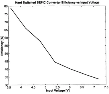
Hard Switched SEPIC Converter Efficiency vs Input Voltage 60 c 55 • 50 5 4 4.5 5 5.5 6 6.5 7 7.5 Input Voltage [V]
Figure 2.2: Efficiency of a hard-switched SEPIC with various input voltages
70% for a 3 W converter, which is simply unacceptable for most (if not all) portable electronic systems. Even if we scale the on-state resistance and the device capaci-tance of the commercial vertical MOSFET (assuming the on-state resiscapaci-tance halves and the capacitance doubles as the device area doubles, and vice versa) to obtain a optimal tradeoff (lowest total loss) between switching loss (given by the first term in equation 2.4) and conduction loss (given by the second term in equation 2.4), the effi-ciency is still only about 74% at the nominal output (See appendix A for component values and simulation files).
In addition, Figure 2.2, which shows the efficiency as a function of input voltage, clearly indicates that performance suffers severely if the converter is to be operating
across a wide input and output voltage range.
2.1.2
Multi-Resonant SEPIC converters
The multi-resonant SEPIC topology [29], fig. 2.3, addresses excessive switching loss by utilizing a multi-resonant network to absorb the parasitic capacitance from the transistor and the diode, and to shape the transistor voltage for zero-voltage turn on. This topology explicitly introduces capacitances in parallel with the switch and
2.2 A New Quasi-Resonant SEPIC Topology
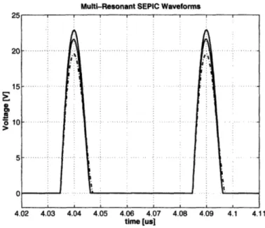
diode along with a resonant inductor Ls in series with the coupling capacitor Cs to achieve zero-voltage soft switching of the switch and diode, as shown in Figure 2.3(b). However, with frequency modulation control, the power stage and control function is tightly coupled, which prevents this converter from maintaining good efficiency as the load condition changes. Figure 2.4 illustrates the operation of the multi-resonant SEPIC converter as the output voltage varies. The multi-resonant SEPIC converter is designed such that the body diode "catches" the ringing across different output voltages. However, using the body diode in such a way can introduce significantly loss due to the diode forward voltage drop. Moreover, when the switch turns on, there is a significant amount of circulating current in the system, introducing yet another loss mechanism that deteriorates the performance. Furthermore, like the conventional SEPIC converters, the bulk inductors limit the response speed of the multi-resonant SEPIC converter.
2.2
A New Quasi-Resonant SEPIC Topology
Here we introduce a new quasi-resonant SEPIC topology, Figure 2.5, suitable for efficient HF resonant power conversion across a wide operating range in addition to providing up-and-down voltage conversion. The topology used here has some topological similarities with both the conventional SEPIC converter [30] and with the multi-resonant SEPIC converter proposed in [31, 29]. However, the detailed component placement and sizing, operating characteristics, and control approach are all very different from these previous designs.
2.2.1
Background
The conventional SEPIC converter has two bulk (ac choke) inductors, and yields hard switching of the switch and diode. The multi-resonant SEPIC [29] utilizes similar bulk inductors, but explicitly introduces capacitances in parallel with the switch and diode along with a resonant inductor in series with the coupling capacitor
CB to achieve zero-voltage soft switching of the switch and diode. Furthermore,
conventional SEPIC converter and multi-resonant SEPIC converter are controlled via frequency modulation. One major drawback associated with frequency modulation control resides in its substantial impact on efficiency under closed-loop operation
SVOUT
(a) A Multi-Resonant SEPIC Converter Topology Multi-Resonant SEPIC Waveforms
Q10 4.05 4.15 -44 4 4.05 4.1 4.15 4.2 4.2 4 4.05 4.1 4.15 4.24.2 201f
Multi-Resonant SEPIC Start-up Transient
LU e
0 10
0 0.5 1 1.5 2 2.5 time [us] 3 3.5 4 4.5(b) Multi-Resonant SEPIC Waveforms
Figure 2.3: A multi-resonant SEPIC converter [29]. ZVS switching characteris-tics are obtained from absorbing device parasitic capacitance by adding external capacitors. Although this converter is not operated under constant frequency, this simulation at 20MHz illustrates the poor transient response due to bulk inductors. See appendix A for component values and simulation files.
-- Vsw --- d(t)
.
...-.
...
... ...
4.25 II fl Lrlll·I····IUI·IIIII1111111111·11·1·1~·· 5I
I·2.2 A New Quasi-Resonant SEPIC Topology
Multi-Resonant SEPIC Waveforms
Figure 2.4: Operation
3V to 7V
4.09 4.1 4.11
of multi-resonant SEPIC as output voltage varies from
due to its tight coupling between the power stage and the control function. As the soft-switching characteristics are closely tied to the impedance of the overall system, any deviation away from this optimal impedance (caused by changes in operating frequency as in the case of frequency modulation) can result in exacerbated circulating current loss and V-I overlap switching loss. Also, at the typical operating frequencies of the frequency conventional SEPIC and multi-resonant SEPIC converter [29], a large amount of output bulk capacitance is needed. This translates to larger size, deteriorated power density and higher cost.
The design introduced here also explicitly utilizes capacitances in parallel with the switch and diode. However, in contrast to previous resonant SEPIC designs [31, 29], the design here has no bulk inductors. Rather, it uses only two resonant inductors: one inductor, LF, resonates with the net switch capacitance, Coss + CEX, for resonant inversion, while the other inductor, LREC, resonates with the rectifier capacitance,
CREC, for resonant rectification. This design method leads to reduced magnetic component count, along with greatly increased response speed.
Operation of this converter can be understood as a linking of three subsystems: a resonant inverter, a matching network and a resonant rectifier (Figure 2.5). A resonant rectifier connected to the inverter via a matching network forms a dc-dc
4.02 4.03 4.04 4.05 4.06 4.07 4.08
VouT
INVERTER MATCHING RECTIFIER
NETWORK
Figure 2.5: Three subsystems of a resonant SEPIC topology
converter when properly tuned can deliver power efficiently at a constant switching frequency and duty ratio. As will be described, the high pass nature of the match-ing/interconnect significantly impacts the system operation.
2.2.2
Converter Design
The design procedure of a full dc-dc converter starts with a rectifier. The rectifier is tuned at the specified output power and voltage to exhibit certain characteristics and behaviors. Once the equivalent impedance at the operating frequency is determined, the rectifier can be replaced with this impedance to a resonant inverter, assuming majority of the output power delivered to the load is transferred at the fundamental. The inverter is then designed following a tuning process described in Section 2.2.5 to achieve desired performance. If the equivalent impedance of the rectifier is too high for a given inverter topology to deliver the required amount of output power, to obtain acceptable efficiency across the whole operating range, or to obtain reasonable component values, a matching network will be necessary to transform the rectifier impedance. The transformed impedance will then be used as the load impedance for the inverter. After a working inverter design is obtained with the equivalent rectifier impedance (with or without a matching network), a full dc-dc converter can simply be obtained by replacing the equivalent impedance with the full rectifier. Additional minor tunings may be required to achieve optimum efficiency and ZVS characteristics due to the interaction between the inverter and the rectifier since the rectifier is a nonlinear device, and is only approximately represented by an equivalent impedance.
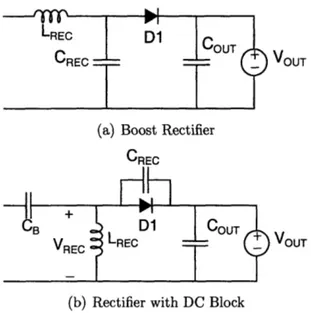
2.2 A New Quasi-Resonant SEPIC Topology LIuv LREC
CREC
T
hJ D1 OUT VOUTT
(a) Boost RectifierCREC
D1
VREC LREc SOUT VoU
7T
(b) Rectifier with DC Block
Figure 2.6: Two resonant rectifier topologies. The boost rectifier can only used in cases where the output voltage is higher than the dc voltage at the rectifier input, and the input provides a dc current path. The rectifier with dc block is
suitable to provide up-and-down voltage conversion.
The following sections will address the detailed tuning of each subsystem and design of a full dc-dc converter by connecting these three subsystems.
2.2.3
Resonant Rectifier
Rectification involves changing ac to dc, which is essential of a dc-dc converter. While classic square wave rectifiers may be a simple and viable solution at low switching fre-quencies, hard-switched rectifiers incur a significant amount of losses when operating at high frequency,. Among them, there are switching losses due to reverse recovery and capacitive charging of the diodes. Furthermore, losses due to low-Q parasitic junction capacitance and package inductance can easily exacerbate the rectifier loss.
It is therefore desirable to design a rectifier topology that provides good efficiency at HF while maintaining a small component count and a small size. While the "series loaded" resonant rectifier [32], Figure 2.6(a) discussed in [3, 33, 32] is a solution proven to meet these three criteria, its inability to provide buck and boost power conversion (due to the de path provided by LREC) makes it an unsuitable candidate
to meet the input and output voltage requirements of this application.
Figure 2.6(b) shows the schematic of the resonant rectifier to be implemented here. This rectifier topology is similar to Figure 2.6(a) except for the change in the location of the resonant inductor and the resonant capacitance. However, this seemingly minor component re-arraignment eliminates the dc path from the rectifier input and enables the topology to be utilized in applications where the output voltage is required to be lower and higher than the dc rectifier input voltage.
2.2.3.1 Basic Operating Principles
The particular resonant rectifier topology of interest here utilizes a resonant tank comprising of a resonant inductor LREC (which provides a dc path for the output current) and a capacitance comprising the external capacitor CREC along with addi-tional parasitic junction capacitance from the diode. To evaluate rectifier operation, the rectifier is driven by sinusoidal current source at the switching frequency, provid-ing an approximate representation of the inverter behavior. The output is modeled as a voltage source of value VOUT, which represents the behavior of the rectifier load when the output voltage is controlled under closed-loop operation. Figure 2.7 illus-trates the rectifier operation via time domain simulation results. VREC is equal to the output voltage when the diode is on; When the diode turns off, LREC and CREC plus junction capacitance resonate until the VREC once again reaches the VOUT. At
turn-off, the voltage across the capacitor equals VOUT and ILREC start decreasing. VREC is
being discharged until the inductor current is lower than the driving current source. Once this condition is reached, ILREC continues to decrease, however, capacitor CREC will start absorbing energy and VREC rings up. Once VREC reaches VOUT, the diode again turns on and the inductor current increases until it exceeds the driving current, then the diode shuts off and the cycle repeats.
2.2.3.2 Rectifier Tuning Procedure
Consider the circuit for rectifier tuning shown in Figure 2.8(a), the amplitude of the current source driving the rectifier is selected such that the output power requirement can be met (Note that a whole range of values may be successfully used). The resonance between LREC and CREC can be selected such that the impedance looking
-2.2 A New Quasi-Resonant SEPIC Topology
Rectifier Voltage and Current Waveforms
I, -10 > -20 4.9 4.92 4.94 4.96 4.98 5 a C. time [us]
Figure 2.7: Rectifier Waveforms
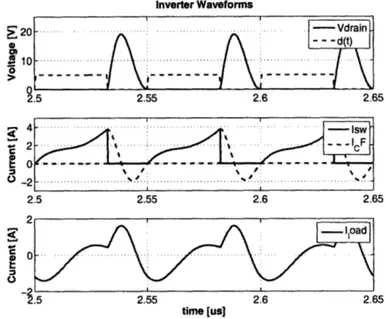
into the input port of the rectifier appear resistive at the fundamental frequency. This equivalent resistance can be readily obtained from the fundamental voltage waveform and the sinusoidal current waveform, Figure 2.8.
A straightforward way to tune this rectifier topology given a specified amplitude of the current source is to adjust CRECT and LRECT until a desired characteristic impedance and center frequency is achieved. The rectifier input impedance can be tuned to look resistive, slightly capacitive or slightly inductive.
To achieve a purely resistive impedance at the fundamental frequency, there are two design handles, the resonant inductor LREC and the resonant capacitor CREC. By adjusting the resonant capacitor along with the resonant inductor, the peak reverse voltage and the length of the conduction interval of the diode can be traded off [27]. While capacitors with Q values in the thousands are relatively easy to obtain, it is much more difficult to obtain small inductors with
Q
of more than 100 at HF. Since it is possible to trade off low-Q inductance with high-Q capacitance to achieve the same impedance, it is generally desirable to do so, as indicated in Figure 2.9 where the rectifier output power and efficiency is plotted for two different values of LREC. It is apparent from Figure 2.9 that a small low-Q inductor with a large high-Q capacitor generally leads to a more efficient rectifier design than a large low-Q inductor with... ..
..
4. .... 4.94.. .96.4.98
.. ...
---.%| | ..Rectifier Voltage and Fundamental
time [us]
(a) Rectifier Tuning Circuit (b) Rectifier Voltage with its Fundamental
Fundamental Rectifier Voltage and Current
Vin V]
(c) Fundamentals of Rectifier Voltage and Cur-rent
Figure 2.8: Rectifier Voltage with its fundamental component extracted. The equivalent impedance of the rectifier can be calculated from the fundamentals of the rectifier voltage and current.The equivalent rectifier resistance REQ is 17.14Qf
CREC
2.2 A New Quasi-Resonant SEPIC Topology
Rectifier Efficiency vs Output Power 92.5 92 91.5 S91 S90.5 89.5 89 88.5 DR 2 2.5 3 3.5 Output Power [W]
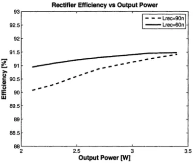
Figure 2.9: Performance comparisons of rectifiers with different values of LRECT.
Better rectifier performance can be obtained by trading off large-valued rela-tively low-Q inductors with large-valued high-Q ceramic capacitance. A switch-ing frequency of 20MHz with an inductor Q of 70 and capacitor Q of 3000 is
assumed in simulations. When LREC = 90nH, CREC is swept from 125pF to 160pF to attain output power from 2W to 3W. When LREC = 60n, CREC is swept from
700pF to 1100pF to achieve similar power levels. Simulation files for this example
may be found in Appendix A
a small high-Q capacitors achieving the same desired rectifier impedance. However, the approach cannot be practiced blindly. Once the required inductance is reduced down to a few nano-henries when the parasitic package inductance and parasitic prototype board inductance (both of which are extremely lossy (low Q) in nature) are on the same order of magnitude as the required resonant inductor, the performance
(waveforms and efficiency) can be tremendously compromised.
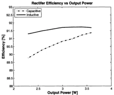
The rectifier can also be tuned to be slightly inductive or slightly capacitive to aid switching. However, for a given output power, the rectifier performance is generally better (more efficient) when it is tuned to be slightly inductive, Figure 2.10. A capacitively-tuned rectifier often has more circulating current loss that deteriorates the performance.
In certain cases, it is more desirable that all of the rectifier capacitance needed by the
- - - Lrec90n ---- Lrec=60n--L -L -· -L -r -r
Rectifer Efficiency vs Output Power 92.5 92 91.5 e 90.5 o , 90 89.5 89 88.5 0n -- .... Capacitive --- Inductive --,
-i
2 2.5 3 3.5 4 Output Power [W]Figure 2.10: Performance comparisons of rectifiers tuned inductively vs capaci-tively. A switching frequency of 20MHz with an inductor Q of 70 and capacitor
Q
of 3000 is assumed in simulations. LREC is kept at 70nH, while the CREC is swept from 260pF to 1200pF to achieve different phases between the fundamen-tal voltage and current. It is obvious that the performance for an inductively tuned rectifier is generally better for a given output power. Simulation files may be found in Appendix Arectifier to be provided by the rectifier device (e.g. a diode) to reduce losses associated with forward conduction drop and to avoid resonances between the capacitors and the device package [27]. However, that external capacitance can achieve much higher Q than lossy parasitic device junction capacitance suggests that adding additional high Q capacitors may result in less losses in some other cases. The decision of whether to add an additional diode in parallel or to add external capacitance entails a careful study of the dominant loss mechanism for each specific design. While in some designs, the circulating current loss associated with the low-Q diode capacitance may be the dominant loss mechanism in a given rectifier; the forward drop associated with the series resistance of the diode may be significant in others. In this case, it is
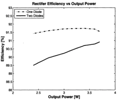
the circulating current that dominates the rectifier loss. Therefore, a better rectifier design can be achieved via adding external high-Q capacitance instead of placing two diodes in parallel, as illustrated in Figure 2.11, where the rectifier performance of utilizing one diode versus two diodes is compared.
2.2 A New Quasi-Resonant SEPIC Topology
Rectifer Efficiency vs Output Power
92.5 92 91.5 2691 E 90.5 o 89.5 89 88.5 AA 2 2.5 3 3.5 4 Output Power [W]
Figure 2.11: Performance comparisons of rectifiers with two diodes vs one diode with additional external capacitance. A switching frequency of 20MHz with an inductor Q of 70 and capacitor Q of 3000 is assumed in simulations. LREC is kept at 70nH, while CREC is swept from 180pF to 300pF when two diodes are employed to achieve similar power levels as the previous plot where only one diode is used. In this case, the performance improvement brought by high-Q external capacitance reducing circulating current losses exceeds the improve-ment brought by reduction in lower forward conduction drop. Simulation files may be found in Appendix A
Although this rectifier topology is highly efficient and simple to tune, it has sev-eral shortcomings. Unlike the rectifier topology in [3], there is no additional tuning knob such as the dc source bias. Instead, once the output power are determined, the properties of the input current source is determined. Changing either the
char-acteristic impedance Zo = / CREC or the center frequency Fc = 21rLRECREcI of the
LC resonance will result a change in the behavior of the rectifier, indicated by the
variations in VRECT waveforms, illustrated in Figure 2.12. Therefore, this topology does not have the flexibility to maintain the overall switching behavior of the rectifier while the characteristic impedance is adjusted up and down, unlike the boost rectifier topology employed in [3].
In addition, as the amplitude of the current source is swept, the nonlinear element (diode and its nonlinear junction capacitance) prevents the impedance from staying
.- - One Diode
S- Two Diodes[
S 0, CL o.r E-Ic 0 0. EI time [us]
(a) Rectifier Waveforms as Fc is swept
3 3.05 3.1
time [us]
(b) Rectifier Waveforms as Zo is swept
Figure 2.12: The rectifier waveforms for various center frequency Fc = 1 and characteristic impedance Zo = LRE. Unlike [3], the
rec-21r LRECT RECT CRECT
tifier does not have the extra degree of freedom from adjusting dc-bias of the source. Therefore, changing either Fc and Zo changes both the current and voltage waveforms. See appendix A for component values and simulation files.
ou 55 50 ~ 45 0 . 40 30 S25 20 15 10
2.2 A New Quasi-Resonant SEPIC Topology
Impedance Phase vs. Output Power
2 2.5 3 3.5 4
Output Power [W]
Figure 2.13: Rectifier Impedance phase (at the fundamental) as a function of
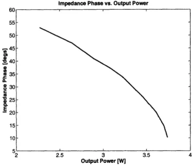
output power. A switching frequency of 20MHz with an inductor Q of 70 and capacitor Q of 3000 is assumed in simulations. Over a wide output power range, changes in the equivalent impedance of the resonant rectifier is significant. Sim-ulation files may be found in Appendix A
purely resistive across different operating conditions. As the amplitude of the current source is increased (the output power is increased), the phase between the voltage and current fundamentals typically increases and the rectifier appears more inductive. On the other hand, as the amplitude of the current sources is decreased (the output power is decreased), the rectifier appears more capacitive indicated by the decreased phase angle between the voltage and current fundamentals. Unlike the high-voltage and high-power rectifier design in [27], this phase change varies significantly across a wide range of output power, as shown in Figure 2.13. This characteristic of the rectifier imposes another challenge on the converter design, requiring an inverter topology that is relatively insensitive to the rectifier phase variation, as will be discussed in Section 2.2.5.
TLMN C
AM
ZLOAD
(a) Low Pass Matching (b) High Pass Matching (c) Low Pass 7r Matching
Net-work work work
LMN LMN LAMN2
CMN ZLOAD CMN ZLOAD
CMN2
(d) High Pass ir Matching (e) Low Pass T Matching Net- (f) High Pass T Matching,
Network work Network
Figure 2.14: Various matching network configurations
2.2.4
Matching Network
The purpose of the transformation stage, a subsystem between the inverter and the rectifier, is to alter the way the rectifier input impedance appears at the output of the inverter, to provide voltage and current level transformation, and to provide elec-trical isolation required by some applications [34]. In some cases, this subsystem is not required. The inverter and the rectifier can be connected merely by adding a dc blocking capacitor, whose capacitive reactance at the switching frequency is substan-tially smaller than the load impedance provided by the rectifier. This transformation stage is useful when the impedance achieved by the rectifier at a given output power level (following the tuning procedure from the previous section) is too high for the inverter to achieve ZVS, provide minimum output power, or operate at acceptable efficiencies. The transformation stage can be realized via conventional transformers, transmission-line transformers, matching network or similar means.
In an application (such as the one pursued in this thesis) where the input impedance provided by the rectifier is too high to deliver the amount of output power required (if to be directly employed at the output of an inverter topology), a matching network which steps down the rectifier impedance is a suitable approach. A matching network is a useful technique to transform impedance with a small number of components and very low loss [35, 34]. A matching network structure is designed to transform a given load impedance to a source impedance at a given frequency. The matching network can take on many forms. Figure 2.14 shows a few examples of matching networks
2.2 A New Quasi-Resonant SEPIC Topology
Matching Network Impedance
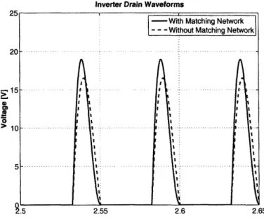
CD M CL E -U0r 0. o OE in 'U 0. U C, El V 0p 0. E, Frequency [MHz]
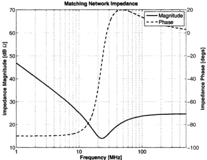
Figure 2.15: Input impedance of a matching network with Figure 2.14(b)
con-figuration. CMN = 720pF, LMN = 70nH and ZLOAD = 17Q.
that reduce the load impedance. The effects that a given matching network has at frequencies besides the switching frequency are very important. Among these match-ing network configurations, the ones that provide a dc path between the inverter and the rectifier such as Figure 2.14(a), 2.14(d), 2.14(f) may be used with an additional dc blocking capacitors to provide up-and-down voltage conversion while others may be employed without any extra components. Also, the way in which these networks pass or block harmonic currents and voltages may greatly affect circuit operation. One consideration in determining the matching network topology relates to the fun-damental operating principle of a matching network. The matching network is de-signed to provide a specific transformation ratio at one frequency, and this frequency only. Since matching networks are comprised of reactive elements, the transformation characteristic is bound to change as the frequency moves away from the frequency at which the matching network is designed. When designing an inverter, the rectifier is modeled by its equivalent impedance(complex ratio of fundamental voltage to fun-damental current) to simplify the design process. Given a rectifier input impedance, a matching network can be designed so that the inverter can achieve some desired output power, efficiency requirement and switching characteristics. However, when the inverter is connected to the rectifier, the matching network now sees the actual
voltage and current waveforms of the rectifier (instead of an equivalent resistance) and the voltages and currents of the rectifier are not scaled by the same transformation ratio across the whole frequency spectrum, which may complicate the tuning proce-dure. For example, Figure 2.15 illustrates a matching network designed to provide a transformation ratio from a 17Q resistive load to 5Q (at the input port of the match-ing network) at about 20MHz. However, it is apparent that the this transformation ratio only occurs at one frequency, with the impedance at other frequencies scaled by completely different complex ratios.
Although different configurations can result in the same impedance transformation ratio at a given frequency, the effect of different matching network topologies on a load impedance won't stay the same across a range of frequencies. A matching network capable of achieving multiple resonances from having more than two reactive elements such as the T and 7r networks has lower efficiency and narrower bandwidth [35], is more prone to completely modifying the rectifier characteristic impedance, and complicates the inverter design even more. Therefore, a simple matching network with minimum component count, such as the one in Figure 2.14(b) is desirable for efficiency, size and volume considerations and converter design and tuning simplicity.
2.2.4.1 Tuning the Matching Network
The first step in matching network design is to determine a configuration. For the reasons mentioned previously, Figure 2.14(b) is a suitable matching network topology for this application, and will serve as a starting point for a matching network design. To determine the transformation ratio required, we can begin by assuming that the drain voltage VDS is a triangle wave (which will be apparent from simulation wave-forms shown in Section 2.2.5.1) with 50 % duty cycle and swings between 0 and 82VIN. If we assume that all the ac power is delivered to the load only at the fun-damental of the switching frequency, the maximum load impedance allowed at the
output of the inverter for a pre-determined output power level is given by
V2
RLOAD
RMS
(2.7)
LOAD- POUT