Helmholtz-Zentrum Berlin für Materialien und Energie, Hahn-Meitner-Platz 1, 14109 Berlin, Germany 2Free University Berlin, Department for Geosciences, Malteserstr. 74-100, 12249 Berlin, Germany 3Zentrum für Sonnenenergie- und Wasserstoff-Forschung, Industriestr. 6, 70565 Stuttgart, Germany 4ETH Zurich, Laboratory of Ion Beam Physiscs, Schafmattstrasse 20, 8093 Zurich, Switzerland 5Thermo Fisher Scientific, Im Steingrund 4-6, 63303 Dreieich, Germany
6Thermo Fisher Scientific, Hanna-Kunath Str. 11, 28199 Bremen, Germany
7Thermo Fisher Scientific, The Birches, Imberhorne Lane, East Grinstead, West Sussex, RH19 1UB, UK 8Thermo Fisher Scientific, Takkebijsters 1, 4817 Breda, The Netherlands
9IFW Dresden, Helmholtzstraße 20, 01069 Dresden, Germany
10Universität der Bundeswehr München, LRT2, Werner-Heisenberg-Weg 39, D-85577 Neubiberg, Germany 11Federal Institute for Materials Research and Testing, Unter den Eichen 87, 12205 Berlin, Germany
12Department of Materials Science & Engineering, University of Illinois, 1304 W. Green St., Urbana, IL 61801, USA 13Catalonia Institute for Energy Research (IREC), C. Jardins de les Dones de Negre 1, 08930 Sant Adrià del Besòs
(Barcelona), Spain
14IN2UB, Departament d’Electrònica, Universitat de Barcelona, C. Martí i Franquès 1, 08028 Barcelona, Spain 15Centre de Recerca i Investigació de Catalunya (CRIC), Trav. de Gràcia 108, 08012 Barcelona, Spain 16ETH Zurich, Department of Chemistry and Applied Biosciences, 8093 Zurich, Switzerland 17Max Planck Institute for Iron Research, Max-Planck-Str. 1, 40237 Düsseldorf, Germany
18Otto-von-Guericke-University Magdeburg, Institute of Experimental Physics, Universitätsplatz 2, 39106 Magdeburg, Germany
19Center for Photovoltaics Innovation and Commercialization (PVIC), University of Toledo, Toledo, OH 43606, USA 20centrotherm photovoltaics AG, Technology Thin Film, Johannes-Schmid-Str. 8, 89143 Blaubeuren, Germany
Abstract: The present work shows results on elemental distribution analyses in Cu~In,Ga!Se2thin films for solar cells performed by use of wavelength-dispersive and energy-dispersive X-ray spectrometry ~EDX! in a scanning electron microscope, EDX in a transmission electron microscope, X-ray photoelectron, angle-dependent soft X-ray emission, secondary ion-mass ~SIMS!, time-of-flight SIMS, sputtered neutral mass, glow-discharge optical emission and glow-discharge mass, Auger electron, and Rutherford backscattering spectrometry, by use of scanning Auger electron microscopy, Raman depth profiling, and Raman mapping, as well as by use of elastic recoil detection analysis, grazing-incidence X-ray and electron backscatter diffraction, and grazing-incidence X-ray fluorescence analysis. The Cu~In,Ga!Se2thin films used for the present compari-son were produced during the same identical deposition run and exhibit thicknesses of about 2 mm. The analysis techniques were compared with respect to their spatial and depth resolutions, measuring speeds, availabilities, and detection limits.
Key words: elemental distributions, comparison, depth profiling, chemical mapping, thin films, solar cells, chalcopyrite-type, Cu~In,Ga!Se2
I
NTR ODUCTIONThin-film research and development is performed on a broad range of materials and on individual layers with thicknesses ranging from a few nanometers to several mi-crometers. For all these cases, it is essential to have access to the compositions of the thin films, which may be divided into concentrations of matrix and trace elements. Since the compositions are frequently not distributed homogeneously
in thin films, and since these elemental distributions may affect the electrical and optoelectronic properties of thin-film devices considerably, the analysis of elemental distribu-tions in thin films is an important issue in both research and industry ~Oechsner, 1984; Reniers & Tewell, 2009!. Further comparisons of techniques for elemental distribu-tion analysis have been reported by Ives et al. ~1997!, Hodoroaba et al. ~2001!, Bohne et al. ~2004!, and Escobar Galindo et al. ~2009!.
In the present work, several techniques providing infor-mation on elemental distributions were employed on about
Received November 5, 2010; accepted April 4, 2011
2 mm thick Cu~In,Ga!Se2thin films from the same identical
deposition run and the same identical Mo/soda-lime glass substrate. Cu~In,Ga!Se2 is used as absorber material in
thin-film solar cells, leading to solar-conversion efficiencies of up to 20.1% ~Jackson et al., 2011!. The present work will focus on the elemental distributions of the matrix elements, particularly those of In and Ga. The techniques are com-pared with respect to their spatial and lateral resolutions, their measuring speeds, their availabilities, and their detec-tion limits.
M
ATERIALS ANDS
AMPLEP
R EPARATIONCu~In,Ga!Se2 thin films ~2 mm! were coevaporated from
elemental sources on Mo-coated ~sputtered, 1 mm! soda-lime glass substrates ~2 mm! by a three-stage process ~Kauf-mann et al., 2005!, which consists of coevaporation of In, Ga, and Se ~stage 1!, deposition of Cu and Se until CuxSe is
formed on top of Cu~In,Ga!Se2~stage 2!, and again
coevap-oration of In, Ga, and Se, until CuxSe is consumed and the
Cu~In,Ga!Se2 layer is Cu-poor. According to the
quasibi-nary Cu2Se-In2Se3phase diagram ~Herberholz et al., 1999!,
single-phase CuInSe2~and also CuGaSe2!is present for Cu
concentrations of about 24–24.5 at.%; i.e., Cu~In,Ga!Se2is
substoichiometric with a certain concentration of Cu vacan-cies, which are responsible for the p-type conductivity.
The Cu~In,Ga!Se2/Mo/glass stacks analyzed for the present work were produced in the identical deposition runs for Mo sputtering and Cu~In,Ga!Se2 evaporation. A
part of the Cu~In,Ga!Se2/Mo/glass stacks were further pro-cessed toward completed solar cells by depositing a CdS buffer layer ~about 50 nm! in a chemical bath and then sputtering a ZnO:Al/i-ZnO bilayer ~with thicknesses of about 40 and 500 nm!. Finally, a Ni-Al grid was deposited on top of the ZnO:Al/i-ZnO bilayer to facilitate the current collec-tion. The reader is referred to Figure 1 for a scanning electron micrograph of a completed solar cell produced from this stack. The solar cells produced in the identical run
as the Cu~In,Ga!Se2/Mo/glass stacks studied for the present work exhibited a conversion efficiency of 16.1% ~average from 21 individual cells with areas of 0.5 cm2!.
Due to substrate rotation during the Cu~In,Ga!Se2
evap-oration, the lateral variations in composition are only about 5 rel.%. The integral compositions of the Cu~In,Ga!Se2thin
films were determined by X-ray fluorescence analysis ~XRF! by use of a Cu~In,Ga!Se2standard, sampling the entire 2 mm
thick films, and given in Table 1.
In general, In and Ga are not homogeneously distrib-uted in Cu~In,Ga!Se2 layers; i.e., the Ga concentration is
larger close to the Mo back contact. Since Cu and Se are generally found to be distributed homogenously across the Cu~In,Ga!Se2layers, the In elemental distribution behaves
inversely to that of Ga.
This compositional distribution may be related to differences in Ga-Se/In-Se and Cu-Se bonding lengths. In-Se is much larger than Cu-Se in CuInSe2, whereas Ga-Se
is quite similar to Cu-Se in CuGaSe2. Corresponding
strain in the Cu~In,Ga!Se2solid solution may induce
diffu-sion of In preferentially toward the surface of the grow-ing Cu~In,Ga!Se2 layer ~Gabor et al., 1994!. Another
possible reason for the formation of the In/Ga gradients in Cu~In,Ga!Se2layers may be the smaller formation enthalpy
for CuInSe2 than for CuGaSe2 ~Cahen & Noufi, 1992!.
Considering that the final Cu~In,Ga!Se2layer first forms by
chemical reactions between the CuxSe compounds
men-tioned above and Cu~In,Ga!Se2at the surface of the
grow-ing thin film ~Klenk et al., 1993!, this is where the compound with the lower formation enthalpy, i.e., CuInSe2, is
prefer-entially present.
In and Ga distributions in Cu~In,Ga!Se2layers have an
impact on their optoelectronic properties because the band-gap energy of CuInSe2 is smaller ~1.04 eV! than that of
CuGaSe2~1.68 eV! ~Alonso et al., 2001!. This will be shown
by the cathodoluminescence results further below; i.e., the In/Ga distributions affect the absorption behavior of the Cu~In,Ga!Se2 layer in its volume. Since the local In/Ga
concentrations in Cu~In,Ga!Se2correlate with the position
of the conduction-band minimum, also the band alignment with the n-type CdS layer ~see Fig. 1! is influenced by the in-depth In and Ga distributions. Dullweber et al. ~2000! showed that the open-circuit voltage of a Cu~In,Ga!Se2
solar cell depends on that band-gap energy that corre-sponds to the Ga concentration close to the surface. More-over, these authors found that the short-circuit density of this solar cell relates to the overall minimum of the band-gap energy, i.e., of the Ga concentration across the Cu~In,Ga!Se2layer.
Figure 1. Cross-sectional scanning electron micrograph of the ZnO:Al/i-ZnO/CdS/Cu~In,Ga!Se2/Mo/glass stack studied for the present work. The solar cell is illuminated from the top.
Table 1. Integral Composition of the Cu~In,Ga!Se2Thin Films Studied for the Present Work, as Obtained by XRF.
@Cu# ~%! @In# ~%! @Ga# ~%! @Se# ~%! 23 6 1 17 6 1 9 6 1 51 6 1
macrostrain can be calculated to about 10 . The corre-sponding macrostrain-related errors are substantially smaller than other possible errors for the determination of peak positions in GI-XRD patterns and Raman spectra. However, for the EBSD patterns acquired across individual grains for the present work, the key issue is the microstrain contained in the grains, which may differ considerably from the macrostrain.
It should be noted that the In/Ga gradients in Cu~In,Ga!Se2layers, formed during the film deposition, are
rather stable. For temperatures lower than about 2008C, no substantial change in the In and Ga distributions is ex-pected, which is the case for all characterization techniques applied in the present work. Also the ion bombardment of the Cu~In,Ga!Se2layers taking place during depth profiling
or cross-section polishing does not affect the In/Ga gradi-ents in the about 2 mm thick films. This fact is apparent when comparing results obtained by secondary neutral mass spectroscopy, performed at liquid nitrogen temperatures, and, e.g., secondary-ion mass spectroscopy depth profiling at room temperature, which both exhibit similar Ga/In elemental distributions.
Possible impurities in Cu~In,Ga!Se2/Mo stacks on soda-lime glasses can be traced back to diffusion from these glass substrates, which consist mainly of SiO2, Na2O,
and CaO. Indeed, Na and O are found to be present in all Cu~In,Ga!Se2films deposited on Mo-coated soda-lime glass,
where Na has an important effect on the charge-carrier den-sity because it may occupy Cu vacancies. Typical Na concen-trations in Cu~In,Ga!Se2films deposited on Mo/soda-lime
glass substrates are about 0.1–3 at.% ~Niles et al., 1997; Gra-nata & Sites, 1998; Rockett et al., 2000!, whereas the integral oxygen concentration is assumed to be substantially lower.
Cross-section samples were produced from a part of the Cu~In,Ga!Se2/Mo/glass stacks in the following way. Two stripes of a sample were glued together face-to-face by use of an epoxy glue. Slices were cut from this stack, and their cross sections were polished mechanically and also by means of an Ar-ion polishing machine ~BALTEC RES-100, at ambient temperature!, using 5 kV and 2 mA at a flat incidence angle of 48. One part of the cross sections was coated by a very thin ~4–5 nm! graphite layer, the other part by a thin ~1–2 nm! gold film. For transmission electron microscopy analysis, the slices were mechanically polished
those techniques that we consider not broadly known in more detail. The descriptions of rather established methods are kept short. We included explanatory schematics and raw data of the measurements where appropriate.
Depth-Profiling Techniques
Secondary Ion Mass Spectrometry
Secondary ion-mass ~SIMS! analysis was conducted in a Cameca IMS 5f instrument with a magnetic sector mass analyzer. Secondary ions were accelerated to an energy of 4,450 eV, energy and mass analyzed, and detected by an electron multiplier or Faraday cup. The sputtering ions were Cs⫹ and struck the sample at an energy of 17 keV. The sputtering beam was about 20 mm diameter and was scanned across a 250⫻ 250 mm area, producing a uniform square crater in the sample. The sputtering ion beam strikes the sample surface at an angle of 308 with respect to the surface normal. The secondary ion yields were obtained by compar-ison with other analysis techniques reported here and with reference to compositions obtained by energy-dispersive X-ray ~EDX! spectrometry in scanning electron microscopy ~see also the Energy-Dispersive X-Ray Spectrometry in a Scanning Electron Microscope subsection below!. The total composition is normalized to 100 at.% for the matrix elements. This normalization results in increased noise in the experimental data. Under ideal measurement condi-tions, transitions of about 10 nm per decade of signal change can be obtained with the Cs⫹ion beam. The depth scale was calibrated by measurement of SIMS crater depths using a Tencor Alpha Step microprofilometer.
A primary advantage of the SIMS technique is its high sensitivity to trace impurities. Mass spectra and depth profiles obtained on this sample showed the presence of common alkali metals including K and Na present through-out the sample and Ca present on the surface but decreasing by two orders of magnitude by about 1 mm deep into the sample. Other impurities in the sample studied included Al and Li ~the latter is not commonly observed! as well as O. Ion yields for all electropositive species show clear rises where oxygen is present. Carbon is commonly found and B may be present in some samples. Other impurities are rare. The resulting profiles determined by SIMS and the other depth-profiling techniques are shown in Figure 2.
of the depth profiles. Sensitivity factors for the quantifica-tion of elements in Cu~In,Ga!Se2 absorbers by SNMS are
well known from earlier calibrations by means of EDX and XRF. To compensate for small changes due to instrumental effects, each elemental distribution profile is fitted to the integral elemental concentration as measured by means XRF ~Table 1!.
SNMS allows an easy and accurate quantification in sputter depth profiling. The reasons are that, for most compounds, more than 98% of sputtered particles are neu-trals, and that the post-ionization efficiency by electron impact is independent of the sample composition. There-fore, the sensitivity factors for the elements are—to a first approximation—fixed values. Due to this separation of par-ticle emission and ionization process, matrix effects as known from SIMS analysis, especially by sputtering with Ar ions, are negligible. As the detection limit for SNMS is in the range of 0.05 at.%, simultaneous SIMS measurements are performed for the detection of trace elements of down to 1 ppm. For example, the incorporation of Na in Cu~In,Ga!Se2
can additionally be detected and roughly quantified by SIMS. In the present work, only the quantitative results from SNMS for the matrix elements in the Cu~In,Ga!Se2
thin film are shown.
The information depth of SNMS and SIMS is only one to three atomic layers and thus extremely low, compared with other methods presented in this comparison. The depth resolution is in the range of several nm depending on the sputter conditions, the depths of the sputter craters, and the material properties. For Cu~In,Ga!Se2 solar cells, the
depth resolution is often limited by the roughness of the layers analyzed, especially of the polycrystalline Cu~In,Ga!Se2
absorber.
X-Ray Photoelectron Spectrometry
The X-ray photoelectron spectrometry ~XPS! analysis of the sample was performed using a Thermo Scientific K-Alpha spectrometer ~Thermo Fisher Scientific, East Grinstead, UK!. Photoelectrons were excited by means of a monochromated Al-Ka X-ray source with a photon energy of 1,486.6 eV. The analysis area on the sample is defined by the size of the X-ray spot at the surface, and a spot size of 150 mm was used in the present work ~the spot size is defined by the distance trav-eled across a Cu knife edge, where the XPS signal intensity
geneous etching. Data were collected and processed using the Thermo Scientific Avantage data system. The data were corrected for the lens-transmission function, and background subtraction was performed using a Shirley function calcu-lated from a numerical iterative method. Each element con-centration was obtained by dividing calculated peak areas by the corresponding Scofield cross section. Etch rates were calibrated against the known thin-film stacking sequence obtained using EDX in scanning electron microscopy ~see description in the Energy-Dispersive X-Ray Spectrometry in a Scanning Electron Microscope subsection further below!.
The strength of the XPS technique lies in its ability to quantify both, elemental and chemical state information, from the top 10 nm or less of the surface of a sample. By using ion beam etching, surface layers can be slowly re-moved, at a rate that is comparable with the probe depth of the XPS technique. This allows profiles to be built up that have good depth resolution and rich information content on the elements present and the chemical environment in which they reside. This makes XPS a powerful technique for examining the chemistry at the interfaces of multilayer devices such as solar cells, where the interaction between adjoining compounds can be of marked contrast to the bulk ~in XPS terms! of the layer. These interactions can have significant influence on the ultimate performance of the device.
Auger Electron Spectrometry
The combination of Auger electron spectroscopy ~AES! as a surface sensitive technique, providing information from the uppermost few nanometers of the sample, with Ar-ion sputtering enables us to detect the depth distribution of elements in the sample. For quantitative analysis, matrix effects that influence the Auger sensitivity of elements in dependence on the surrounding material have to be taken into account. Possible changes of the sample composition at the surface due to Ar ion sputtering have to be corrected. Furthermore, Ar-ion bombardment may lead to depth-profile distortions due to surface roughening and/or com-positional intermixing.
The Auger spectra were acquired at a primary electron energy of 5 keV in the dN/dE mode with a modulation voltage of 4 V and lock-in detection. The electron beam was scanned across an area of 100 mm⫻ 100 mm. The electron
energy analyzer was a PHI Mod. 15-155 cylindrical mirror analyzer. Ar-ion sputtering was performed by use of 4 keV Ar⫹ions at an angle of incidence of about 508 with respect to the surface normal. Quantification was performed by relating the averages of the signal intensity distributions to the integral concentrations given in Table 1.
By means of AES, it is possible to determine chemical states of the elements. Due to the small information depth of about 1–3 nm, buried interface layers may be detected when AES is combined with sputter depth profiling. The knowledge about composition at interfaces of multilayer systems is important for the optimization of the perfor-mance of devices as the solar cells studied for the present work.
Glow-Discharge Optical Emission Spectrometry
The glow discharge optical emission spectrometry ~GD-OES! represents a rapid depth-profiling technique capable of qual-itative and quantqual-itative elemental analysis of bulk and lay-ered samples ~Payling & Jones, 1993; Bengtson, 1994; Angeli et al., 2003!. The sample atoms are sputtered in the glow discharge cell under voltages of 600–1,500 V in the atmo-sphere of inert gas ~usually argon!. Then, they are excited by plasma species and emit light of certain wavelengths. This characteristic emission is detected by a spectrometer.
The glow discharge can be powered by direct current ~dc! or by radio frequency ~rf! voltage in a continuous or pulsed mode. By means of rf discharge, also nonconducting samples can be analyzed. The rf mode is more often applied for thin-film analysis, e.g., because of less intense plasma ignition.
For the analysis of nearly all elements ~including light elements H, C, N, O! in the films of 1 nm up to more than 100 mm thickness, GD-OES has shown its advantages of high depth resolution ~5–10% of layer thickness for layers with thicknesses .3 nm!, high sensitivity ~0.1–100 mg/g!, and high dynamic range ~ mg/g up to main components!. The crater shape and consequently the depth resolution must be optimized by variation of the discharge parameters ~rf voltage, Ar gas pressure, pulse frequency, and duty cycle!. The easy application of GD-OES is caused by the experimen-tal simplicity ~e.g., no ultrahigh vacuum is required! and results in high sample throughput.
The disadvantage of the method is low lateral resolu-tion restricted by the anode diameter. To reduce contamina-tions of water and hydrocarbons absorbed at inner walls of the glow discharge source and the sample surface, low evacuation pressure ~ pe⫽1 ⫻10⫺5mbar! and a low leakage
rate ~3.9⫻ 10⫺6mbar L/s! were used. Before each measure-ment, the discharge cell was evacuated ~30 s! and flushed with pure argon gas ~30 s!.
The GD-OES analysis of the Cu~In,Ga!Se2sample was
carried out using a Spectruma GDA 750 spectrometer equipped with a 4-mm Grimm-type rf source. As a power supply the Spectruma free running rf generator ~6.7 MHz! was used in the regime of constant voltage and pressure ~800 V, 1.8 mbar!. When brittle samples with low heat
conductivity ~i.e., glass! are analyzed, softer conditions are needed. In such cases, a pulsed rf discharge may be applied to reduce the introduced power per time. In the present work, pulsed rf discharge was used because of the glassy substrate ~pulse frequency 1,222 Hz and duty cycle 4%!. The measuring duration for the Cu~In,Ga!Se2/Mo stack was 750 s.
The characteristic emission was detected by means of a Spectruma Paschen-Runge type polychromator ~2,400 grooves per mm, 750 mm diameter of the Rowland circle, resolution 0.02 nm! and an Ocean Optics S2000 CCD spectrometer ~wavelength: 200–1,100 nm, resolution 0.5 nm!. The used emission lines were 207.478 nm ~Se!, 324.754 nm ~Cu!, 379.734 nm ~Mo!, 417.204 nm ~Ga!, 450.094 nm ~In!, 588.995 nm ~Na!, where the Mo and Na signals are not shown in the present work. Enhanced Na signals are found in the Mo layer and at the Mo/glass interface. Quantifica-tion of Cu, In, Ga, and Se signals was performed by relating the averages of the signal intensity distributions to the integral concentrations given in Table 1.
Glow-Discharge Mass Spectrometry
The Thermo Scientific ELEMENT GD used in this study is a double-focusing high-resolution mass spectrometer, which features a fast flow GD DC source using argon carrier gas flows of about 400 mL/min. The combination of detectors allows measurements of ultra traces up to matrix elements over a linear dynamic range of 12 orders of magnitude ~from 0.2 to larger than 1012counts/s for the matrix signal!. Ultra
traces and matrix elements can be measured within a single analysis because the detection system switches between de-tection modes within 1 ms. Typical sensitivities are on the order of 1010counts/s for the matrix signal. The main
com-ponents of the glow discharge mass spectrometry ~GD-MS! are sample holder, plasma chamber, ion optic assembly, mag-net, electrostatic analyzer, and detection system. As for GD-OES, the sample ~approximately 20 mm diameter! acts as a cathode, and a differential potential is generated between the anode and the cathode in the plasma chamber. Owing to the high electric field in the sample surface, Ar ions are accelerated toward the sample surface, and various kinds of ionization processes occur. The sample ions are then acceler-ated and focused before entering the magnetic field. They are separated by the analyzer according to their ratios M/z ~mass of the element divided by its charge!. The intensity of the element signal relative to the matrix signal allows for quantification of the concentration of each element.
The discharge current, gas flow, and voltage were ad-justed to achieve sufficient signal intensity ~of the order of 107counts/s for the matrix signal!, while using soft sputter
conditions ~lower discharge current compared with bulk analyses! to achieve a good depth resolution. The sputter rate for the experiment is about 5 nm/s. As the present study focuses on the depth profile of matrix components, only the most sensitive low-resolution mode was used. Any possible interference can be neglected in view of the much more intense matrix signals.
The discharge voltage applied was 650 V, the discharge current 6.5 mA, and the discharge gas flow 450 mL/min. Prior to analyzing the sample, the required isotopes to be detected for the elements of interest as well as the scan and integration durations for the selected isotopes were deter-mined. Care was taken to achieve the maximum scan speed available ~approximately seven scans per s!. Each data point shown in the GD-MS data in Figure 2 represents an average of three scans.
The low current used was also favorable to avoid break-ing the glass substrate due to local thermal stress from the glow discharge. As an additional measure, the Peltier cool-ing device of the instrument was switched to heatcool-ing mode, so that the sample was kept at 408C to achieve a smaller heat difference between sputtered area and the rest of the sample. Data acquisition was started simultaneously with the glow discharge. The resulting profile indicated that the sample substrate was reached after 750 s. For each scan, the instrument yielded a semiquantitative concentration for the matrix elements analyzed.
The basic principle for evaluation in GD-MS is based on ion-beam ratios ~IBR! and relative sensitivity factors ~RSF!. For each scan, the measured intensities for each isotope are normalized to the total ion beam measured. These IBR are multiplied with a sensitivity factor ~RSF! to calculate concentrations. As is common practice in GD-MS, also unknown samples can be analyzed semiquantitatively by using a default set of RSF values. This standard RSFs table was determined for a steel matrix but can also be applied semiquantitatively to other sample compositions. Typical errors introduced are 630 rel.%. As a consequence for time resolved analysis, each data point shown has been quantified based on the default sensitivity factors, according to the IBR measured at this point. Although absolute sensi-tivity may vary over the sputter time, according to the composition of the corresponding layers, the normalization to the total matrix current and subsequent proportional use of RSF values is a valuable approach for depth profile analyses.
Raman Depth Profiling
Raman scattering measurements were performed using a Horiba Jobin-Yvon T64000 spectrometer with an Ar⫹laser excitation source ~514.5 nm! in backscattering configura-tion. The penetration depth of scattered light in CuInSe2is
estimated to below 100 nm, assuming an absorption coeffi-cient at the given wavelength of 105 cm⫺1 ~Firoz Hasan
et al., 1999!. The focused spot size on the surface of the samples was about 100 mm, with an excitation power of 20 mW. In-depth resolved measurements were performed by acquiring sequentially a series of Raman spectra after sputtering the sample with the Ar⫹beam from a Phi 670 scanning Auger nanoprobe ~Álvarez-García et al., 2001!. To minimize damage in the sputtered region, the energy of the Ar⫹beam during ion sputtering was below 5 keV.
The sputter rate can be estimated taking into account that the time required to sputter the whole Cu~In,Ga!Se2
layer is about 53 min. Assuming a thickness of about 1.8 mm ~from the results obtained by EDX in transmission electron microscopy, see the Energy-Dispersive X-Ray Spec-trometry in a Transmission Electron Microscope subsection below!, the sputter rate results in about 34 nm/min.
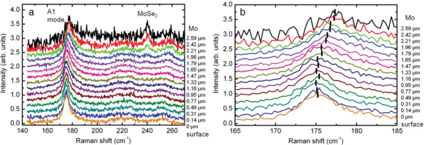
Figure 3 shows the Raman spectra measured after sput-tering the surface of the layer at different depths. All the spectra are normalized to the intensity of the main peak corresponding to the Cu~In,Ga!Se2A1mode, and the
spec-tra measured after various sputter durations are vertically shifted. A contribution to these spectra at the 150–170 cm⫺1 region is visible, which is characteristic for the damage induced by the sputter process. This damaging also induces slight broadening of the peak. However, measurements per-formed in reference samples show not any influence of this process on the position of the main A1mode. The spectrum
acquired after 50 min sputtering exhibits the presence of modes at about 169 and 240 cm⫺1that are characteristic for the MoSe2layer present between Mo and Cu~In,Ga!Se2.
Fitting of these spectra with a Lorentzian curve allows determination of the main A1peak of Cu~In,Ga!Se2. This
A1 peak shifts toward higher frequencies with increasing
Figure 3. a: Raman spectra measured after sputtering the layer down to various depths ~these spectra are shifted vertically!. b: Enlarged section from panel a, between 165 and 185 cm⫺1. Peak shifts of the A1mode with increasing sputtering depths are apparent ~the maxima of the peaks are highlighted by ticks!.
depth ~Fig. 3b!, which is directly related to the increase in the local Ga content in the Cu~In,Ga!Se2alloy toward the
interface with the Mo back contact. Raman scattering mea-surements performed with the same experimental setup on reference CuInSe2 and CuGaSe2 layers give values for the
frequency of the A1 mode of 173 cm⫺1 ~CuInSe2! and
183 cm⫺1~CuGaSe2! ~Rincón & Ramírez, 1992; Caballero
et al., 2010!. In the case of a Cu~In,Ga!Se2alloy, the position
of the A1 mode shows a linear dependence on the relative
Ga content. It increases linearly with the @Ga#/~ @In#⫹ @Ga#! ratio from the position corresponding to CuInSe2 ~ @Ga#/
~ @In#⫹ @Ga#! ⫽ 0! to that characteristic of CuGaSe2~ @Ga#/
~ @In# ⫹ @Ga#! ⫽ 1! ~Tanino et al., 1993!. This allows for obtaining an estimation of the in-depth @Ga#/~ @In#⫹ @Ga#! distribution, and therefore the distributions of @In# and @Ga# in the layers are determined assuming constant Cu and Se distributions and that @Cu#⫹ @In# ⫹ @Ga# ⫹ @Se# ⫽ 1 in the layers.
In the interpretation of the present Raman spectros-copy data, we also assume that there are not any disorder or stress effects present in the Raman spectra affecting the frequency of the A1mode. Higher in-depth spatial
resolu-tions ~up to the order of 100 nm! can be achieved by decreasing the sputter duration between consecutive Raman scattering measurements because of the high light absorp-tion in Cu~In,Ga!Se2.
Nondestructive Techniques
Rutherford Backscattering Spectrometry
Helium-4 Rutherford backscattering spectrometry ~RBS! measurements ~Chu et al., 1978! were performed at the PSI/ETH EN tandem accelerator at beam energies of 2 and 5 MeV. Backscattered He ions were detected by a Si detector under an angle of 1658. The sample was tilted by 108 against normal incidence.
RBS with He has the advantage that elastic scattering cross sections and specific energy loss of these ions in mate-rials are well known. As a consequence, the measured stoichi-ometries and the depth scale of concentration profiles are accurate to better than 5%. The main disadvantage is the insufficient mass resolution to separate Cu and Ga and the fact that the interpretation of the data is not unambiguous due to the superposition of all concentration depth profiles in one single spectrum. This ambiguity can be partly re-solved by using different scattering or target tilt angles and different beam energies. A measurement at 2 MeV beam energy yields the composition at the very surface of the sample, though with very limited mass resolution. With a beam energy of 5 MeV, the He ions penetrate the whole layer, and the mass resolution is 2.5 times better than at 2 MeV. Since the depth scale in RBS is compressed with increasing beam energy, the depth resolution is worse at 5 MeV, though. Even at 5 MeV, the ambiguity of interpreta-tion of the profile is not completely resolved.
To obtain the In in-depth distribution profiles, the stoichiometric numbers of Se and Cu have been set to 2 and
1. Then a number of six sublayers of various @Ga#/@In# ratios were fitted to the spectrum by the RUMP simulation software ~Doolittle, 1986!. By the total energy loss of He ions in the Cu~In,Ga!Se2layer, the thickness is estimated to
be approximately 2.1 mm. Helium-4 energies higher than 5 MeV may not be used because scattering cross sections start to be “non-Rutherford,” and nuclear resonances and reactions become possible.
To enhance the separation of Cu and Ga at the sample surface, heavy-ion backscattering has been performed with 15 MeV28Si projectiles. A high-resolution annular gas
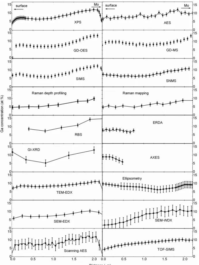
ion-ization detector was used to detect backscattered particles under an angle of 1768. These measurements confirmed the Ga/In ratio found by He-RBS at the layer surface ~approxi-mately 0.5 mm!. In addition, the assumption about the Cu and Se concentrations was confirmed as well in this depth range. The resulting profiles determined by RBS and the other nondestructive techniques are shown in Figure 4.
Heavy Ion Elastic Recoil Detection
Heavy ion elastic recoil detection ~HI-ERD or HI-ERDA! measurements ~L’Ecuyer et al., 1976! were performed at the Munich Tandem accelerator using a DE-Eresdetection
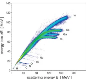
sys-tem described in Bergmaier et al. ~1998!. ERD using swift heavy ions has the advantage that elastic scattering cross sections and specific energy loss of these ions in materials are well known. As a consequence, the measured stoichiom-etries and the depth scale of concentration profiles are as accurate as better than 5 rel.%. See Figure 5 for the raw data of the ERD measurements.
The technique is most suitable for the analysis of light and medium heavy elements ~1ⱕ Z ⱕ ⬃30, where Z is the atomic number! in thin layers. A depth resolution of about 10 nm can be achieved with common detection techniques due to the large stopping forces of the heavy ion beams. On the other hand, these large stopping forces also limit the measurable sample thickness, especially if an elemental dis-crimination of heavy target elements is required, as in the case of the Cu~In,Ga!Se2layer.
For the analysis of the Cu~In,Ga!Se2layer, an ion beam
of 310 MeV197Au was prepared, which is the most heavy ion
beam at maximum energy possible at the Munich accelera-tor. The incident angle of the beam ions was 208 with respect to the sample surface; the elastically scattered sam-ple atoms were detected at an angle of 388. From the energy spectra of the individual elements, quantitative depth pro-files were calculated using the computer code KONZERD ~Bergmaier et al., 1995!.
Angle-Dependent Soft X-Ray Emission Spectroscopy
Angle-dependent X-ray emission spectroscopy ~AXES! is a nondestructive, photon-in, photon-out technique that pro-vides depth-dependent information on the elemental com-position of a sample. It also yields the chemical environment of the probed atoms. However, this information is not used in the context of the present work. To obtain sufficient intensity and tunable excitation energy, synchrotron
radia-tion is desirable as an excitaradia-tion source. Thus, the experi-ments were conducted at the U 41 PGM beamline at the BESSY electron storage ring. The emitted radiation was analyzed using a Gammadata Scienta XES-300 soft X-ray grating spectrometer. The information depth ranges from a few tens up to hundreds of nanometers, depending on the relative sample tilt angle, the excitation and emission ener-gies, as well as the absorption behavior of the sample. When changing the sample tilt angle and keeping all other factors constant, elemental-distribution depth profiles can be ex-tracted from the integrated intensities of the emission peaks. In the used set-up, the angle between excitation and detec-tion is fixed at 908, while the exit angle b is used to control
the information depth ~see Fig. 6!. A minimum information depth can be obtained at grazing incidence ~br 908! and grazing exit ~br 08! geometries, while between these ex-tremes, a maximum of information depth is obtained. To achieve a higher accuracy and to minimize effects due to roughness, relative peak intensities are evaluated at a series of different exit angles b. This implies that the results monitor exclusively relative concentrations.
In our investigation of the depth-dependent elemental distributions of Cu~In,Ga!Se2 thin films, we recorded
Cu-L3M4,5, Ga-L3M4,5, and In-M4,5N2,3emission peaks at
vari-ous emission angles b and used relative intensities to calculate the @Cu#/~ @Ga#⫹ @In#! ratios as a function of sample depth. Figure 4. Elemental distributions acquired by means of “nondestructive” techniques.
To limit the extensive measurement time, we did not mea-sure within an additional energy window covering the Se-L3M4,5 emission line. At excitation energies of 1,200 and
1,080 eV, a minimum information depth below 30 nm is obtained, while the maximum information depth is around 500 nm. With this, AXES covers a depth range that is difficult to probe by other nondestructive techniques.
To extract the depth profiles shown in Figure 4, we assumed the sum of the concentrations @Cu# ⫹ @Ga# ⫹ @In#⫹ @Se# to be 1 ~no Se emission was measured!, and we assumed the ratio of cations to anions ~ @Cu# ⫹ @Ga# ⫹ @In# !/@Se# to also be 1. A more detailed description of the technique and the modeling procedure is given in Mönig et al. ~2008, 2010!.
Grazing Incidence X-Ray Diffraction
The quantitative evaluation of grazing incidence X-ray diffraction ~GI-XRD! is a nondestructive method for the analyses of in-depth elemental distribution profiles. The underlying idea is to calculate the shape of diffraction signals from a tentative set of compositional depth profiles and compare this simulated result with the measured data. The depth profiles are then modeled in an iterative proce-dure to fit the shape of the calculated reflections to the measured data ~Kötschau & Schock, 2003, 2006!.
Diffraction signals of Cu~In,Ga!Se2 thin films with
Ga/In compositional gradients generally show broadened, asymmetric peak shapes. This stems from the fact that the
lattice plane distances—and therefore the 2u position of a reflection—are influenced by these compositional gradients of this solid solution; i.e., in Cu~In,Ga!Se2 thin films, the
reflection position is a function of the layer depth. ~Conse-quently, only those compositional variations affecting the lattice parameters considerably can be resolved.!
The actual depth information of the method stems from the attenuation of the radiation within the sample. The penetration depth of the radiation and consequently the shape of the diffraction signals depend on the incidence angle of the X-ray beam. By a variation of the incidence angle, the contribution of a diffraction signal from a certain depth is varied.
The GI-XRD patterns of the absorbers were collected on a Panalytical X’Pert MPD Pro system with Cu-Ka radia-tion ~l⫽ 1.54056 Å! and a nickel Cu-Kb filter. To focus the parallel beam, a 1/168 divergence slit and a 2 mm mask was used. The instrumental profile was defined by the measure-ment of a standard Si tablet, with the same configuration as used for the Cu~In,Ga!Se2thin film, at various incidence
angles ~0.5, 1.0, 1.5, 2.0, 2.5, 3.0, 4.0, and 5.08! at 2u ranging from 25 to 1008. Each of these Si patterns were refined by the Rietveld method, and single peak fits with a pseudo-Voigt function were applied to the 111 reflection. The position of the 111 reflection in the 2u range is close to the 112 reflec-tion of Cu~In,Ga!Se2. Therefore, it was possible to
deter-mine the full-width at half-maximum accurately in this 2u range, which is substantial for the extraction of composi-tional gradients by X-ray diffraction methods.
The presented calculation of the diffraction signals were performed by use of the simulation software TFXDAU. For a detailed description of this method, please refer to Kötschau and Schock ~2006!. The top layer of the sample was assumed to purely consist of Cu~In,Ga!Se2as
confirmed by XRD measurements. The thickness of the Cu~In,Ga!Se2 layer was set to 2 mm, according to the
scanning electron microscope ~SEM! image ~see Fig. 1!. For the simulation of the diffraction signals, the Cu~In,Ga!Se2
layer was divided into 100 sublayers. For each sublayer, the Cu~In,Ga!Se2112 reflection peak was calculated from the
assumed average composition of this sublayer using a pseudo-Voigt peak shape. The intensity of the peak from each sublayer was determined by the attenuation of the radiation due to mass absorption by the overlying sublayers depending on the incidence angle. Finally, the peaks of all sublayers are summed up to obtain the resulting total diffraction signal for a given incidence angle. The intensity of the total diffraction is additionally influenced by sample size and geometry of the setup. To rule out deviations between measured and calculated data stemming from these factors, the calculated diffraction signal intensities were scaled to agree with the signal intensities of the measured data.
For the data evaluation presented in this work, an automated fit routine was programmed to determine the parameters of the Ga depth profile. The number of these parameters was set to 5. Each parameter gives the atomic Figure 5. Raw data of the ERD measurement. The energy loss of
the detected sample elements is plotted versus their scattering energy. Apart from the matrix elements ~Cu, In, Ga, Se!, various further impurities ~H, C, N, O, Si, Na! were detected.
Figure 6. Elemental distributions acquired by means of “nonde-structive” techniques.
ratio @Ga#/~ @Ga#⫹ @In#! for a certain point of layer depth z. The z values were held constant. The distance of the z values increases exponentially with the layer depth due to a de-crease of sensitivity of the method with the depth. The complete course of the depth profile was determined by linear interpolation between the parameter points. The @Ga#/ ~ @Ga#⫹ @In#! values for each parameter point were deter-mined by a least-squares fit. The error square between simulated and measured diffraction data was minimized by a fit routine based on the Levenberg-Marquardt method ~Levenberg, 1944; Marquardt, 1963!.
Only the in-depth distribution of the ratio @Ga#/ ~ @Ga#⫹ @In#! was modeled by the fit routine. The Se and the Cu depth profiles were set constant. The ratio @Cu#/ ~ @Ga#⫹ @In#! was set to 0.88 according to the XRF measure-ments ~Table 1!. The ratio @Se#/~ @Cu#⫹ @Ga# ⫹ @In#! was set to 1. The In in-depth distribution profile was calculated under the assumption that the concentrations of all matrix elements sum up to 100 at.%.
In Figure 7 the measured diffraction data for the Cu~In,Ga!Se2112 reflection for various incidence angles are
shown together with the corresponding simulated data. The graph shows a good agreement between the measured and the calculated data.
A decrease of the ratio @Cu#/~ @In#⫹ @Ga#! has a similar effect on the position of the 112 reflection as an increase of the ratio @Ga#/~ @In#⫹ @Ga#!. Therefore, by taking only the 112 reflection into account for the depth profile modeling, it is not possible to model both the Ga and the Cu depth profile. As a consequence, the Cu depth profile was set constant. If the Cu depth profile is changed, the Ga depth profile resulting from the least-squares fit would change as well. For example, if one assumed a decrease of the Cu content near to the surface of the sample, the simulation of the Ga profile would exhibit a lower Ga content near to the surface. This uncertainty can be solved by taking further reflections into account because changes in the Ga and Cu contents influence the Cu~In,Ga!Se2 lattice constants in a
different manner ~Stephan et al., 2009!. Other properties such as domain size, microstrain, and macrostrain may also influence the reflection shape. An investigation of the reso-lution limits and the extension of the method to multireflec-tion modeling will be published elsewhere ~R. Mainz, unpublished!.
Ellipsometry
Over the past few decades, spectroscopic ellipsometry has emerged as a nondestructive, noninvasive optical technique for characterization of the structure and optical functions of thin film solar cell materials and devices ~Boccara et al., 1993; Collins et al., 1998!. Ellipsometry derives its name from the measurement of the output polarization ellipse that is generated after a beam of light with a known input polarization ellipse has interacted with a sample, most com-monly in a specular reflection configuration.
The very rough surfaces of Cu~In,Ga!Se2thin films at
the thicknesses ~1–2 mm! used in high quality photovoltaic devices imply that reference dielectric function determina-tion for uniform films of various Ga and In ratios can be particularly challenging due to the suppression of the specu-larly transmitted and reflected light waves via scattering from the thin-film surfaces ~Marsillac et al., 2010!. When the surface roughness layer is very thick, the light beam may not penetrate very deeply into the bulk layer, particularly for high photon energies. In addition, typical optical models for the surface roughness that work well in describing thin ~,10 nm! layers are oversimplified for the thick ~.30 nm! roughness layers. Rather than a single roughness layer de-scribed as an effective medium of 0.5/0.5 ~bulk material/ void!, a multilayer designed to simulate a surface region with graded void volume fraction ranging from 1 at the surface to 0 at the interface to the bulk is likely to serve as a better approximation. Because the surface roughness in-creases in thickness during film growth, one method for avoiding this problem is to perform measurements during film growth and to limit the total thickness of the film to Figure 7. Measured ~circles! and simulated ~dashed lines! data for the Cu~In,Ga!Se2112 reflection for various incidence angles. The simulated diffraction peaks correspond to the Ga distribution shown in Figure 4 ~GI-XRD data!.
less than 100 nm ~Walker et al., 2009!. Another method for modeling of films with significant surface roughness is to perform the measurements at multiple angles of incidence so that a larger number of free parameters can be obtained with greater confidence. Throughout the present study, three angles of incidence, 658, 708, and 758, were used for reference dielectric function determination of uniform lay-ers and for depth-profiling analysis of the compositionally-graded Cu~In,Ga!Se2layer.
Spectroscopic ellipsometry data were acquired using a commercially available variable angle spectroscopic ellipsom-eter ~Johs et al., 2001! in the rotating-compensator configu-ration with multichannel detection ~Lee et al., 1998!. The photon energy range of the instrument is 0.75–6.50 eV. Pairs of ~c, D! spectra were collected with an acquisition time of 10 min at each angle of incidence. Experimental data were first collected on uniform reference Cu~In,Ga!Se2
films, each film having a different value of the @Ga#/@In# ratio, but a uniform composition as a function of depth into the thin film. These data were analyzed using software based on a least-squares regression algorithm. This software determines the bulk and surface roughness thicknesses as well as the bulk layer dielectric functions that generate c and D datasets serving as best fits to the experimental datasets. In this analysis, the dielectric function of the surface roughness layer was deduced from that of the bulk layer by applying the Bruggeman effective medium approx-imation ~EMA! assuming a 0.5/0.5 volume fraction mixture of bulk material and void ~Fujiwara et al., 2000!. With this approach, the resulting dielectric functions can be further fit assuming a single analytical expression based on optical transitions between parabolic bands in the neighborhood of the band structure critical points ~Collins & Ferlauto, 2005!. The best fit parameters in the expression, including not only the band gaps but also amplitudes and broadening param-eters, are plotted as a function of the known @Ga#/@In# ratio for the set of samples, and these plots are fit using polynomi-als. Thus, in the analysis of the graded layer, the @Ga#/@In# ratio can be used directly as a free parameter because it uniquely defines the dielectric function through the poly-nomial coefficients, which generate the required analytical expression.
With this database, the optical model for the film with the graded structure can be established. This model consists of three major layers including bulk molybdenum, which acts as the substrate; the absorber layer, which was divided into 36 sublayers; and a surface roughness layer, which was modeled as usual by a 0.5/0.50 volume fraction mixture of the underlying sublayer material and void. The dielectric function of each sublayer was linked to the alloy composi-tion as described in the previous paragraph.
The analysis of the graded absorber layer was per-formed in two steps. In the first step, the near surface composition in six sublayers was determined from the high energy ~.2 eV! region of data where the light has a limited penetration depth. ~Taking CuInSe2 as an example, the
inverse absorption coefficient, or penetration depth, at 2 eV
is given by a⫺1 ⫽ 140 nm, and information can only be extracted from a depth of about 3a⫺1, or about 400 nm for energies of 2 eV and greater.! In the second step, the composition of the top surface was fixed at that deduced from the high energy range. Then the low energy range of 0.75–2 eV, which includes light that penetrates throughout the entire absorber layer structure, is used to extract the composition of the underlying 30 sublayers.
The first analysis step allowed for the determination of the Cu~In,Ga!Se2surface roughness layer thickness of ds⫽
21.2 6 0.3 nm, and the second analysis step provided the bulk layer thickness of db⫽ 2,224.8 6 0.5 nm for the graded
Cu~In,Ga!Se2 absorber. Uncertainty in the analysis of the
@Ga#/@In# ratio profile arises because a different reference set of samples fabricated at the University of Toledo was used to establish the relationship of the dielectric function to @Ga#/@In# ratio. As long as this reference set of samples is also of device quality, the assumption is likely to be a good one; however, the deduced optical parameters, most impor-tantly the fundamental ~or lowest energy! band gap param-eter built into the analytical expression, are more basic results of the analysis and not dependent on such uncertain-ties. To establish the molar compositional profile from the @Ga#/@In# ratio profile for the graded layer, fixed copper and selenium contents of 23 and 51 at.% ~see Table 1! were assumed throughout the depth. Hence, although the @Ga#/@In# ratio can be determined through the entire thick-ness of the film, no information is currently provided by spectroscopic ellipsometry on the content or on the profile of Cu and Se. Such information may be extracted in the future if a reference dataset is available with a dielectric function expression that includes parameters depending on both, the alloy ratio and the Cu content. Finally, it should be pointed out that ex situ depth profiling of this type by spectroscopic ellipsometry is a significant challenge. This challenge can be overcome more easily through the use of real time spectroscopic ellipsometry, which has been dem-onstrated to provide composition profiles with subnano-meter resolution ~Fujiwara et al., 1998; Podraza et al., 2008!.
Techniques Performed on Cross Sections
Energy-Dispersive X-Ray Spectrometry in a Scanning Electron Microscope
Cu, In, Ga, and Se distribution profiles across the Cu~In,Ga!Se2layer were extracted from corresponding EDX
maps ~256⫻196 pixels! acquired by use of a Thermo Noran X-ray detector and the Thermo Fisher Scientific software Noran System Six in a LEO GEMINI 1530 SEM, which is equipped with a field-emission gun. It has been shown ~Barkshire et al., 2000! that spatial resolutions of down to 100 nm and below may be obtained in SEM-EDX measure-ments by reducing the acceleration voltage down to few kV. One prerequisite is that the acceleration voltage still is sufficient to excite the signals of all elements of interest in a sample, where in the present case, it is the In-L line, which exhibits the highest energy of the L lines of all matrix
elements, of about 3.4 keV. To achieve a considerably high intensity of the In-L line, the acceleration voltage was set to 7 kV ~beam current about 6 nA!. A second prerequisite is that the EDX evaluation software is able to deconvolute effi-ciently Cu-L and Ga-L signals, which is presently the case for software packages provided by various manufacturers.
The given signals in Figure 8 are net counts, i.e., the background was subtracted, and the peaks were fitted and deconvoluted. The SEM-EDX signals were quantified by calculating average net intensity values for each of these across the Cu~In,Ga!Se2layer and relating these averages to
the integral compositions determined by XRF ~Table 1!.
It is shown by the SEM-EDX data in Figure 8 that the local maxima in the Ga distribution profile located close to the Mo layer and near to the surface ~or to the CdS/ZnO layers! are revealed, similarly as for the transmission elec-tron microscope ~TEM!-EDX ~Fig. 8! and the XPS ~Fig. 4! results. Thus, although the spatial ~and depth! resolution is substantially worse for SEM-EDX compared with various other techniques, this method is able to measure elemental distributions of thin films with thicknesses of down to 30 nm ~see, e.g., Abou-Ras et al., 2011!. Naturally, the X-ray signals from very thin layers are broadened owing to the generation profile of the incident electron beam at ~for Figure 8. Elemental distributions acquired by means of cross-section techniques.
example! 7 keV. It is noteworthy that SEM-EDX may also be performed on fractured cross sections, e.g., if thin films are deposited on glass substrates ~Kaufmann et al., 2009!.
Wavelength-Dispersive X-Ray Spectrometry in a Scanning Electron Microscope
The Thermo Fisher Scientific parallel beam spectrometer MagnaRay was used to perform net count line scans of the elements Cu, In, Ga, and Se. The acceleration voltage was set to 20 kV, which enabled a free choice of lines over the energy detection range up to 12 keV with a standard equip-ment of four flat crystals ~NiC80, TAP, PET, LiF!. The MagnaRay spectrometer uses a patented hybrid X-ray focus-ing optic incorporatfocus-ing both a capillary and grazfocus-ing inci-dence optic combined with a low-energy capable sealed xenon proportional counter for achieving high throughput. The adjustment of the atomic number Z is facilitated by use of an automated direct drive at an angular precision better than 10⫺38.
Fifty single spectra were acquired during the line scan for each element. The dwell time for each point was set to 5 s. The LiF diffractor was chosen for the analysis of Cu-K, Ga-K, and Se-K. In-L was measured using a PET diffractor. The given signals in Figure 8 are net counts, i.e., the back-ground was subtracted, and the peaks were fitted and decon-voluted. Similarly as for SEM-EDX, the SEM–wavelength dispersive X-ray ~WDX! signals were quantified by calculat-ing average net intensity values for each of these across the Cu~In,Ga!Se2 layer and relating these averages to the
inte-gral compositions determined by XRF ~Table 1!.
The WDX measurements reveal the same trend as the EDX measurements. It can therefore be assumed that statis-tically reliable results are obtained in a few minutes for each element.
One main advantage of WDX spectrometers lies in the ability to detect approximately one power of ten smaller amounts of trace elements, compared with EDX. The con-centration ranges of the Cu~In,Ga!Se2solar cell are in an
order of magnitude that also allows good-quality EDX measurements.
Another major advantage of WDX compared with EDX is better energy resolution. This is often very important for the correct identification of element lines that cannot be separated by EDX.
Energy-Dispersive X-Ray Spectrometry in a Transmission Electron Microscope
Elemental distribution profiles of Cu-K, Ga-K, Se-K, and In-L signals were acquired across the Cu~In,Ga!Se2layer by
use of the Thermo Fisher Scientific Noran System Six acqui-sition software and a liquid N2-cooled Thermo Noran X-ray
detector at a Zeiss LIBRA 200 FE TEM. It is the advantage of TEM-EDX as compared with SEM-EDX that the TEM lamella prepared for the present study was quite thin ~about 30–50 nm at the position of analysis!, i.e., the excitation volume was quite small and thus the achievable spatial resolution high, about 2 nm. We estimate, however, the
actual spatial resolution slightly larger to about 5 nm, as estimated from the decrease of signals at the interfaces to CdS/ZnO and to Mo.
The acceleration voltage applied was 200 kV, the point-to-point distance 20 nm, the total number of points 100, and the dwell time 5 s. The signals given in Figure 8 are net counts, i.e., the background was subtracted, and the peaks were fitted and deconvoluted. Similarly as for SEM-EDX, the TEM-EDX signals were quantified by calculating average net intensity values for each of these across the Cu~In,Ga!Se2layer and relating these averages to the
inte-gral compositions determined by XRF ~Table 1!.
While the analysis of elemental distribution in about 2 mm thick layers is not difficult to perform by means of TEM-EDX, it is challenging to study interdiffusion at the nanometer scale between the various layers in the solar-cell stack ~e.g., Abou-Ras et al., 2005! or also elemental distribu-tions within individual layers ~e.g., Platzer-Björkman et al., 2006!. Presently, spatial resolutions in TEM-EDX measure-ments as high as 0.4–0.6 nm may be achieved by use of aberration-corrected microscopes ~Watanabe et al., 2006!.
Scanning Auger Electron Microscopy
The test specimen is excited by bombardment with elec-trons to emit Auger elecelec-trons. These elecelec-trons refer to the uppermost approximately 5 nm of the surface and are detected by use of an electron spectrometer consisting of an energy analyzer and an electron detector system. The mea-sured energies of the Auger electrons can be correlated to corresponding elements.
A PHI 700 scanning Auger spectrometer manufactured by Ulvac-PHI, Inc. ~Kanagawa, Japan! was used for the present analysis. The Auger electron emission was excited by a primary electron beam of 10 kV at 1 nA. The size of the analyzed area on the sample was about 5 mm ⫻ 5 mm. Surface contaminations that suppress Auger signal intensi-ties were removed by 22 s sputtering with 3 keV Ar⫹-ions on an area of 0.8 mm⫻ 0.8 mm at a beam current of 2 mA. To compensate for charging effects, the sample was tilted to 608 with respect to the surface normal and flooded by 70–90 eV Ar⫹ions. By applying these conditions, line scans of Ga, Se, Cu, In, Zn, O, Mo, Si, and S were acquired on the cross-sectional sample of the ZnO/CdS/Cu~In,Ga!Se2/Mo/ glass solar-cell stack. Quantification was performed by relat-ing the averages of the signal intensity distributions to the integral concentrations given in Table 1.
Time-of-Flight Secondary-Ion Mass Spectrometry
Time-of-flight secondary-ion mass spectrometry ~TOF-SIMS! is applied for qualitative determination of atomic and molecular composition of the top surface layers. The sample surface is bombarded by a primary ion beam ~Ga⫹, Au⫹, In⫹, Bi⫹, Cs⫹, oxygen, or noble gas ions!, which creates an atomistic collision cascade into the bulk. Due to ener-getic transfer the atomic lattice of the near surface region ~one to two atomic layers! is destroyed, and atoms as well as molecular fractions leave the surface. Most of emitted
parti-~SIMS⫹! as well as O, S, Se, Si, AlO2, CSO, Cu2O2, GaO, and
MoO3~SIMS⫺! were detected ~note that the Ga isotopes for
the primary beam and for the TOF-SIMS signals are differ-ent, i.e., possible Ga implantations do not affect the measure-ment results!. The line scans given in Figure 8 ~TOF-SIMS! are averages from several individual line scans extracted from elemental distribution maps. Quantification was performed by relating the averages of the signal intensity distributions to the integral concentrations given in Table 1.
Raman Mapping
A cross-sectional sample of the ZnO/CdS/Cu~In,Ga!Se2/Mo/ glass solar-cell stack was investigated using a combined atomic force microscopy ~AFM! and Raman ‘NTegra Spec-tra’ system ~NT-MDT, Zelenograd/Moscow, Russia!. The upright microscope system is equipped with a 100⫻/ N.A. ⫽ 0.7 long-working distance objective with an AFM module mounted between objective and sample. Design of the ob-jective and shape of AFM cantilevers ~“nose-type” ATEC cantilevers, Nanosensors, Neuchatel, Switzerland! allow si-multaneous AFM and optical measurements on the exactly same part of transparent and opaque samples. The system is equipped with a white-light microscope module and with a video camera for observation and rough alignment of the sample, a confocal scanning microscope module with photo-multiplier tube detector for laser-based imaging, and a spectrometer with four different interchangeable gratings and CCD detector ~Newton, Andor, Belfast, Northern Ire-land, UK! for Raman measurements. The system is con-trolled by the NT-MDT Nova software, which allows simultaneous AFM imaging and Raman mapping experi-ments. All measurements for the present study were per-formed using a 632.8 nm HeNe laser, which was attenuated to a power of approximately 0.5 mW at the sample using neutral density filters in the NTegra Spectra system. This laser power did not lead to detectable sample damage or change of Raman spectra, which has been verified by apply-ing measurement durations 2–120 times longer than for the Raman results shown in the present work. No changes in band positions or relative intensities were found.
AFM imaging and Raman mapping were performed on the identical part of a cross-sectional ZnO/CdS/ Cu~In,Ga!Se2/Mo/glass sample in semicontact mode ~“tap-ping mode”!. By scanning the sample through the laser
tion was acquired on the cross-sectional sample. Instead of the 600-line standard grating ~approximately 1.2 cm⫺1 spec-tral resolution!, an 1,800-line grating with a resolution of approximately 0.4 cm⫺1was applied. This was necessary to detect small band shifts close to the Cu~In,Ga!Se2/Mo interfaces. The gain in spectral resolution was accompanied by an approximately ten times smaller signal intensity and a three times smaller spectral range. The latter was not a limiting factor in this study. A line scan of 10 mm across the sample was performed with a lateral resolution of 128 pixels or approximately 80 nm per pixel. The collection time per pixel was 300 s, leading to a total measurement time per line of more than 10 h.
Figure 9 shows selected Raman spectra collected during the line scan. The spectra were background corrected, and the intensities of the most prominent bands at 175 cm⫺1 ~Witte et al., 2009a! were normalized to 1 for better compa-rability. Also, the spectra were stacked by introducing offsets of 0.2. For the Cu~In,Ga!Se2band at 175 cm⫺1, small band
shifts can be detected close to the interface to the Mo layer. Also, an additional band at 240 cm⫺1appears close to the edge, which can be assigned to MoSe2.
Information on the stoichiometry of Cu~In,Ga!Se2can
be derived from the Raman shifts or exact band positions ~see also the Raman Depth Profiling subsection above!. The raw data show steps corresponding to the spectral resolu-tion of approximately 0.4 cm⫺1. Smoothed data were ob-tained by fitting a Lorentz-type function to each A1 band
and plotting its position versus distance ~see Fig. 8!. Band shifts of up to 2.5 cm⫺1are detected at distances of approx-imately 1 mm from the Mo layer, related to the increasing Ga content toward the interface with the Mo back contact. The In and Ga in-depth distribution profiles can be derived taking into account the linear dependence of the frequency of the A1mode on the @Ga#/~ @In#⫹ @Ga#! ratio, similar to
the procedure described in the Raman Depth Profiling subsection above.
C
OMPARISON OF THEG
AD
ISTRIBUTIONSO
BTAINED BY THEV
ARIOUST
ECHNIQUESTo compare the Ga distribution profiles obtained by the methods presented in the previous section, they are shown in Figure 10. To provide comparability between all these
results, the spatial scales were adjusted such that the Cu~In,Ga!Se2 layer thickness was 2 mm. Most of these
profiles feature a larger Ga concentration close to the Mo back contact than close to the surface ~or to the CdS/ZnO layers!. While ERDA and AXES were able to provide elemen-tal distributions only down to depths of 800 and 500 nm, the ellipsometry result shows a slightly higher Ga concentra-tion close to the surface of the Cu~In,Ga!Se2 layer than
close to the Mo layer. XPS, GD-OES, GD-MS, TEM-EDX, and SEM-EDX exhibit clearly the presence of a local maxi-mum in the Ga distribution close to the surface, which is also indicated ambiguously by the RBS, the GI-XRD, the AXES, and the ellipsometry results.
It is definitely challenging for the application of the techniques that the Ga concentration varies only slightly on a length of about 2 mm, between about 7 at.% close to the surface and about 12 at.% close to the Mo layer, with a local minimum of about 6 at.% ~taking the XPS result as refer-ence!. For thin films with substantially larger compositional variations on similar length scales, several of the techniques compared in the present work, e.g., SNMS, have shown better performances ~e.g., Hodoroaba et al., 2001!. It should also be mentioned that ERDA and AXES are very useful techniques especially for very thin films of few hundreds of nanometers, which are outperformed by several other tech-niques when applied on the total thickness of few microme-ters thick layers.
D
ISCUSSIONAn important question for us to answer was which tech-nique is best to measure elemental distributions in thin films. We conclude that, after evaluating the data obtained by the various techniques, we were not able to identify any method that would be able to determine satisfactorily the quantitative elemental distributions across a layer with un-known composition. For precise quantitative elemental dis-tribution analysis with accuracy of 1 at.% and below, it is
necessary to consult yet another technique for verification of elemental distributions or for quantification of the ac-quired data.
For the elemental distributions obtained by most of the techniques, the average signal intensity distributions were calibrated by means of the XRF measurement ~Table 1!; such a calibration was not necessary for Raman depth profiling and mapping, as well as for RBS, ERDA, GI-XRD, AXES, and ellipsometry. This indicates that one approach of a quantitative elemental distribution analysis may be to acquire the net-count intensity distribution and use an integral quantitative measurement as a reference. Also for measuring the qualitative distributions, it is helpful to em-ploy more than only one technique because such an individ-ual result often remains ambiguous, with uncertainties concerning measurement artifacts and limitations impeding a high quality of the resulting elemental distributions.
All measurement techniques that were presented above have their advantages and disadvantages, and it is the spe-cific requirements of the elemental distribution analysis that determine which method to choose. A first general remark concerns the analysis geometry. Depth-profiling tech-niques and those that are termed “nondestructive” in the present work, both analyzing the thin film from the top, do not require any sample preparation and give ~in part! infor-mation on elemental distributions in short time. However, if thin films exhibit substantial compositional variations in their lateral extensions, it may be more favorable to look at cross-sectional samples.
Several of the techniques presented in this work use ion sputtering generating craters in the thin film. Roughness at the borders of the craters affect the measurement results substantially, and the sputter yield also may change for varying in-depth phase compositions. Thus, it is necessary to adjust for these effects by, e.g., rotating or cooling the sample as well as by post-processing the data. Often, sputter conditions need to be adjusted specifically for a material system under investigation.
Figure 9. a: Raman spectra collected in a line scan across the Cu~In,Ga!Se2layer in a solar-cell stack. Only each second spectrum of all acquired is shown. The lateral distances are given on the right side of the spectra. A MoSe2band close to the interface to the Mo layer is visible. b: Enlarged section of panel a, between 165 and 185 cm⫺1. Note the shift of the A1 band, indicating increased Ga concentrations when moving from the surface ~0 mm! to the Mo layer ~2.59 mm!.
Figure 10. Ga distributions across Cu~In,Ga!Se2obtained by various techniques. The surface is positioned left from 0 mm, the Mo layer right from 2.2 mm. The lines in the graphs are guides for the eye. The error bars are estimates individually for each technique. Note that these error bars do not overlap for all techniques and for all positions; i.e., it can generally not be stated that the “real” concentration values are to be found within the intervals given by the error bars.