HAL Id: hal-00976041
https://hal.archives-ouvertes.fr/hal-00976041
Submitted on 9 Apr 2014
HAL is a multi-disciplinary open access
archive for the deposit and dissemination of
sci-entific research documents, whether they are
pub-lished or not. The documents may come from
teaching and research institutions in France or
abroad, or from public or private research centers.
L’archive ouverte pluridisciplinaire HAL, est
destinée au dépôt et à la diffusion de documents
scientifiques de niveau recherche, publiés ou non,
émanant des établissements d’enseignement et de
recherche français ou étrangers, des laboratoires
publics ou privés.
Volume charge carrier number fluctuations probed by
low frequency noise measurements in InN layers
Geeta Rani Mutta, Jean-Marc Routoure, Bruno Guillet, Laurence Méchin,
Javier Grandal, Sara Martin-Horcajo, Tomaso Brazzini, Fernando Calle,
Miguel A. Sanchez-Garcia, Philippe Marie, et al.
To cite this version:
Geeta Rani Mutta, Jean-Marc Routoure, Bruno Guillet, Laurence Méchin, Javier Grandal, et al..
Volume charge carrier number fluctuations probed by low frequency noise measurements in InN
layers.
Applied Physics Letters, American Institute of Physics, 2011, 98 (25), pp.252104-1–3.
�10.1063/1.3601855�. �hal-00976041�
Volume charge carrier number fluctuations probed by low frequency noise
measurements in InN layers
Geeta Rani Mutta,1,2,a兲Jean Marc Routoure,2Bruno Guillet,2Laurence Méchin,2 Javier Grandal,3 Sara Martin-Horcajo,3 Tommaso Brazzini,3 Fernando Calle,3 Miguel A. Sánchez-García,3Philippe Marie,1and Pierre Ruterana1
1CIMAP, UMR 6252, CNRS–ENSICAEN–CEA–UCBN, 6, Boulevard du Maréchal Juin,
14050 Caen Cedex, France
2
GREYC, UMR 6072, CNRS–ENSICAEN–UCBN, 6, Boulevard du Maréchal Juin, 14050 Caen Cedex, France
3
Instituto de Sistemas Optoelectrónicos y Microtecnología and Dept. de Ingeniería Electrónica,
E.T.S.I. Telecomunicación, Universidad Politécnica de Madrid, Ciudad Universitaria, 28040 Madrid, Spain 共Received 16 March 2011; accepted 1 June 2011; published online 21 June 2011兲
Bulk conduction in molecular beam epitaxial InN layers has been confirmed using low frequency noise measurements versus temperature. A generation-recombination process has been identified at low temperaturesⱕ100 K and attributed to a trap with a discrete energy level in the band gap. The energy position of this trap has been determined to be around 52 meV below the conduction band minimum. © 2011 American Institute of Physics. 关doi:10.1063/1.3601855兴
During the last decade indium nitride 共InN兲 has been the subject of intense research, which led to the redefinition of its band gap from 1.89 to 0.69 eV, and pointed out its many interesting properties, such as the smallest electron effective mass,1 the largest mobility,2 and the highest peak and saturation electron drift velocities among the known semiconductors.1Therefore, InN has emerged as a promising candidate for high speed electronic and optoelectronic appli-cations up to terahertz frequencies.3Despite these properties of InN, there are still many challenges for device fabrication which are related to material’s quality, but also to the pres-ence of an intrinsic charge accumulation at surfaces.4 In some cases, the presence of this electron accumulation layer may be of interest for sensor applications.5
There are many reports on surface charge accumulation in InN layers, including the measurements of sheet carrier density as a function of InN film thickness and capacitance-voltage 共C-V兲 profiling.4 Photoemission measurements in InN with Ti or Au contacts showed that it was not possible to form Schottky contact, the authors concluded that the Fermi level was always located in the conduction band.6The exis-tence of an electron accumulation layer on clean InN共0001兲 surfaces has been confirmed by high resolution electron en-ergy loss spectroscopy 共HREELS兲 and x-ray photoemission spectroscopy.7 Angle-resolved photoemission spectroscopy was used to observe quantized energy levels in the surface electron accumulation layer on InN films grown by radio frequency plasma-assisted molecular beam epitaxy.8 Bhatta et al.9reported the presence of charge accumulation on high pressure chemical vapor deposited InN layers by using HREELS and suggested that the excess surface electron ac-cumulation presence in InN was not due to excess indium or In–In bonds. This is consistent with the pinning of the sur-face Fermi level in the conduction band.10 As was shown during the past few years, the surface Fermi energy in InN is pinned at 0.9 eV above the bottom of the conduction band by donorlike surface defects, which creates an n-type
accumu-lation layer at the surface that seems unaffected by chemical or physical treatments.11Obviously, the conductivity of this surface layer has to be considered in any investigation of the electrical properties of InN samples. Most recently, electro-lyte based chemical C-V measurements have been used to point out a net concentration of ionized acceptors below the n-type surface and demonstrated the possibility of InN p doping using Mg acceptors.12
In this work, we have carried out low frequency noise 共LFN兲 measurements in the 77–300 K temperature range on patterned InN films. In the following, we show that such measurements constitute a convenient tool to access the InN band gap, to investigate the conduction mechanisms and to relate them to the bulk and surface transport properties.
The investigated InN films were grown on c-plane sap-phire substrate by plasma assisted molecular beam epitaxy 共PA-MBE兲. The wafers consisted of the following multilayer structure: first, a commercial LUMILOG semi-insulating Ga polar GaN layer共5 m兲 grown by metalorganic vapor phase epitaxy on sapphire substrates served as a template. The PA-MBE then started with the growth of a 90 nm thick GaN layer and the InN layer was grown on top with a nominal thickness of 345 nm. Structural investigations show that such layers are of substantially good crystalline quality.13In order to characterize the electric transport properties of these InN layers, a stack of metals Ti/Al/Ni/Au 共20 nm/40 nm/20 nm/80 nm兲 was deposited using e-beam evaporation and an-nealed at 400 ° C during 15 min in a N2 flow. Films were
photolithographically patterned and processed by reactive ion etching to form transmission line method 共TLM兲 struc-tures. As shown in the inset of Fig.1, each device was made of three TLM structures, of which we used TLM共a兲 consti-tuted of a series of contact pads 共area 94⫻48 m2兲, with spacings of 38, 57, 114, 170, and 210 m. The TLM pat-terns allowed us to determine both the contact and the InN layer sheet resistance. Direct current共dc兲 and noise measure-ments were performed using a four probe configuration setup in the 77–300 K temperature range with a Lakeshore TTP4 prober. The dc electrical resistivity and LFN measurements were carried out using a HP 4156B semiconductor parameter
a兲Electronic mail: geeta-rani.mutta@ensicaen.fr.
APPLIED PHYSICS LETTERS 98, 252104共2011兲
0003-6951/2011/98共25兲/252104/3/$30.00 98, 252104-1 © 2011 American Institute of Physics
analyzer and a homemade low noise electronics read out as-sociated with a 3562A Dynamic Signal Analyzer,14 respec-tively. The home made amplifier uses junction field effect transistor based operational amplifiers with negligible input current noise thus enabling the measurement of a large range of resistance values. At 300 K, the device LFN is close to one hundred times higher than the electronic readout noise for the lowest value of the current used in this work. At each temperature, the dc resistance R and the LFN voltage spec-tral density Sv共from 10 Hz to 100 kHz兲 were measured for different dc bias currents.
The current-voltage 共I-V兲 characteristics of InN TLM patterns were also measured at various temperatures. We had an Ohmic behavior for both the InN material and the metallic contacts in the whole temperature range. The contact and InN sheet resistance values were extracted from the mea-sured resistance as a function of spacings between metallic pads. The measured contact resistance was always 103times smaller compared to the measured InN resistance. A decrease in the electrical resistivity with decreasing temperature down to approximately 130 K was observed for each characterized device, as illustrated for one device in Fig. 1. The tempera-ture dependence of the resistance above 130 K showed, for all the devices, a positive temperature coefficient of about 7.70⫻10−4 K−1 at 300 K, which is in agreement with
re-ported results in InN nanowires.15 This resistivity depen-dence with temperature is characteristic of a metal-like con-ductor in contrast to a nondegenerate semiconcon-ductor.15,16
In order to better understand the physical mechanisms behind the transport properties in our unintentional doped InN layer, noise measurements at different temperatures T have been carried out. LFN sources and especially 1/f noise sources are related to mobility fluctuations共charge carrier兲 in the bulk17 or number fluctuations which usually originates from the surface.18
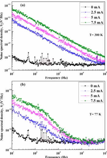
Figure 2 shows two examples of typical noise spectral densities Sv as a function of frequency for different bias currents. These measurements were performed on a 94 m wide and 210 m long bridge at 300 K关Fig.2共a兲兴 and 77 K
关Fig. 2共b兲兴. Before each noise measurement at different currents and temperatures, the resistance of the devices was systematically measured to check that it did not vary in the considered bias current range as a consequence of self heating.
In Figs. 2共a兲 and 2共b兲, two different trends were ob-served above and below 100 K. Above 100 K up to 300 K range, the spectra clearly consisted of following two parts: a 1/f noise contribution that depends on the bias current and frequency, and the white noise part which remains constant 关Fig. 2共a兲兴. For each temperature the measured white noise
level was in agreement with the dc electrical resistance ac-cording to 4kBTR, where kB is the Boltzmann constant. The
slope of the low frequency part was around ⫺1 in the 10– 100 Hz frequency range, thus confirming the “1/f” behavior. We checked the quadratic dependency of Sv versus the bias current共0 to 7.5 mA兲, as expected in homogeneous samples. From this dependency, it was possible to calculate the figure of merit␣ for the 1/f noise level19which is the product of
␣ the Hooge parameter andthe carrier mobility at 300 K. This figure of merit is around 100 cm2V−1s−1 for our sample at 300 K 关corresponding to Fig. 2共a兲兴 which is four orders of magnitude higher than those reported for poly Si or Ge for instance.20This shows that even for MBE samples, as the growth parameters are critical21 small deviations from optimal conditions may have a substantial impact on device performances as shown, in this instance, by the LFN mea-surements.
At lower temperatures 共ⱕ100 K兲, apart from the 1/f noise and white noise, a Lorentzian shape appears with a characteristic frequency fcand plateau levels that depend on FIG. 1. 共Color online兲 The electrical resistivity of the InN layer between
300 and 77 K increases with temperature above 100 K, with a clear linear behavior above 130 K, which is an indication of a metallic behavior. The inset is a schematic of the TLM patterns used for the measurements.
FIG. 2. 共Color online兲 Voltage noise spectral densities measured for differ-ent dc bias currdiffer-ents:共a兲 300 K 共R⬃79 ⍀兲, the curves are dominated by the 1/f noise contribution with the usual slope of⫺1. 共b兲 Apart from the white and 1/f noise contributions, at 77 K共R⬃71 ⍀兲, a Lorentzian contribution is now visible.
252104-2 Mutta et al. Appl. Phys. Lett. 98, 252104共2011兲
the temperature 关Fig.2共b兲兴. The characteristic frequency of the Lorentzian curves did not depend on the bias current and it decreased when the temperature was reduced.22 Conven-tionally, this Lorentzian profile is attributed to a generation recombination process due to a trap that has a discrete energy level in the band gap. A single relationship= 1/2fcexists
between the time constantof the trap and the characteristic frequency of the Lorentzian.23 The Arrhenius diagram ob-tained by plotting ln共⫻T2兲 as a function of 1/共k
BT兲 is
shown in Fig.3. For all the devices under study, the results were identical and showed a clear linear dependence. The energy level of the trap was deduced from the slope of the linear fit, its energy position being around 52 meV below the conduction band minimum. As a consequence, these results can be interpreted as a transition from nondegenerated 共be-low 100 K兲 to a degenerated semiconductor. For temperature higher than 100 K, only 1/f noise is observed and the elec-trical resistivity increases with the temperature: InN acts like a metallic conductor and no single trap generation recombi-nation process can be observed. Below 100 K, Lorentzians appear and electrical resistivity is more or less constant with the temperature: InN acts as a semiconductor. It was possible to probe a bulk trap thus indicating the part of the electrical conduction occurs in the bulk; a volume charge carrier num-ber fluctuations was thus probed by the LFN measurements. Apart from the Lorentzian behavior, an increase in one decade in the 1/f noise level with temperature from 77 K up to 300 K is observed. In order to explain this behavior, basic models for homogeneous sample were tested in order to dis-tinguish between number and mobility fluctuations with ei-ther intrinsic or constant doping of free carriers. The most convincing one was the number fluctuations model with a constant doping of the free carriers. This model could ex-plain the increase in the 1/f noise level with temperature indeed. As this model is often linked to surfaces, this fact is consistent with the presence of a free carrier accumulation layer at the surface reported by other techniques.4,6–10 As usual for 1/f noise interpretation, a more detailed analysis
and model should be necessary to propose a clear conclusion on this fact.
In summary, LFN measurements were performed on MBE grown InN layers from 77 K up to 300 K. The increase in the 1/f noise level with the temperature may be a confir-mation of the electron accumulation layer at the surface which was already reported by other techniques. However, the Lorentzians observed at or below 100 K and the evolu-tion of their characteristic frequencies with temperature are consistent with a generation-recombination mechanism due to a discrete trap level which has been determined at 52 meV below the conduction band. These results show that with the present technique, it is possible to probe the part of the elec-trical conduction that takes place in the bulk of InN films.
The authors acknowledge the support by the EU under the Grant Agreement No. PITN-GA-2008-213238, Initial training network RAINBOW of the 7 RTD Framework.
1A. G. Bhuiyan, A. Hashimoto, and A. Yamamoto,J. Appl. Phys.94, 2779
共2003兲.
2K. I. Lin, J. T. Tsai, T. S. Wang, J. S. Hwang, M. C. Chen, and G. C. Chi, Appl. Phys. Lett. 93, 262102共2008兲.
3V. M. Polyakov and F. Schwierz,Appl. Phys. Lett. 88, 032101共2006兲. 4H. Lu, W. J. Schaff, and L. F. Eastman,J. Appl. Phys. 96, 3577共2004兲. 5H. Lu, W. J. Schaff, L. F. Eastman, and C. E. Stutz,Appl. Phys. Lett. 82,
1736共2003兲.
6K. A. Rickert, A. B. Ellis, F. J. Himpsel, H. Lu, W. Schaff, J. M. Redwing,
F. Dwikusuma, and T. F. Kuech,Appl. Phys. Lett. 82, 3254共2003兲.
7T. D. Veal, I. Mahboob, L. F. J. Piper, C. F. McConville, H. Lu, and W. J.
Schaff,J. Vac. Sci. Technol. B 22, 2175共2004兲.
8L. Colakerol, T. D. Veal, H. K. Jeong, L. Plucinski, A. DeMasi, T.
Lear-month, P. A. Glans, S. Wang, Y. Zhang, L. F. J. Piper, P. H. Jefferson, A. Federov, T. C. Chen, T. D. Moustakas, C. F. McConville, and K. E. Smith, Phys. Rev. Lett. 97, 237601共2006兲.
9R. P. Bhatta, B. D. Thomas, M. Alevli, and N. Dietz,Surf. Sci. Lett. 601,
L120共2007兲.
10W. Walukiewicz,Physica B 302–303, 123共2001兲.
11I. Mahboob, T. D. Veal, C. F. McConville, H. Lu, and W. J. Schaff,Phys. Rev. Lett. 92, 036804共2004兲.
12X. Wang, S. B. Che, Y. Ishitani, and A. Yoshikawa,Appl. Phys. Lett. 91,
242111共2007兲.
13A. Vilalta-Clemente, G. R. Mutta, M. P. Chauvat, M. Morales, J. L.
Doualan, P. Ruterana, J. Grandal, M. A. Sanchez-Garcıa, F. Calle, E. Val-cheva, and K. Kirilov,Phys. Status Solidi A 207, 1079共2010兲.
14J. M. Routoure, D. Fadil, S. Flament, and L. Méchin, AIP Conf. Proc.
922, 419共2007兲.
15C. Y. Chang, G. C. Chi, W. M. Wang, L. C. Chen, K. H. Chen, F. Ren, and
S. J. Pearton,Appl. Phys. Lett. 87, 093112共2005兲.
16T. Richter, H. Lüth, T. Schäpers, R. Meijers, K. Jeganathan, S. Estèvez
Hernández, R. Calarco, and M. Marso, Nanotechnology 20, 405206 共2009兲.
17F. N. Hooge and L. K. J. Vandamme, Phys. Lett. A 66, 315共1978兲. 18A. L. Mcwhorter, Ph.D. thesis, 1/f noise and related surface effects in
germanium, Massachusetts Institute of Technology, 1955.
19C. Liang, G. Leroy, L. K. J. Vandamme, and J. L. Wojkiewicz,Synth. Met.
159, 1共2009兲.
20L. K. J. Vandamme and H. J. Casier, Proceedings of the 34th ESSDERC,
Leuven, edited by R. P. Mertens and C. L. Claeys共IEEE, Piscataway, NJ, 2004兲, p. 365.
21C. S. Gallinat, G. Koblmüller, J. S. Brown, and J. S. Speck,J. Appl. Phys.
102, 064907共2007兲.
22N. B. Lukyanchikova, Noise and Fluctuations Control in Electronic
Devices, edited by A. Balandin共American Scientific, California, 2002兲, p. 201.
23V. Grassi, C. F. Colombo, and D. V. Camin,IEEE Trans. Electron Devices
48, 2899共2001兲. FIG. 3. The Arrhenius diagram obtained by plotting ln共⫻T2兲 as a function
of 1/共kBT兲, a trap energy level of 52 meV below the conduction band
mini-mum is obtained.
252104-3 Mutta et al. Appl. Phys. Lett. 98, 252104共2011兲