HAL Id: hal-03013414
https://hal.archives-ouvertes.fr/hal-03013414
Submitted on 18 Nov 2020
HAL is a multi-disciplinary open access
archive for the deposit and dissemination of sci-entific research documents, whether they are pub-lished or not. The documents may come from teaching and research institutions in France or abroad, or from public or private research centers.
L’archive ouverte pluridisciplinaire HAL, est destinée au dépôt et à la diffusion de documents scientifiques de niveau recherche, publiés ou non, émanant des établissements d’enseignement et de recherche français ou étrangers, des laboratoires publics ou privés.
Solvent Molecules
Ye Wang, Amine Slassi, Jérôme Cornil, David Beljonne, Paolo Samori
To cite this version:
Ye Wang, Amine Slassi, Jérôme Cornil, David Beljonne, Paolo Samori. Tuning the Optical and Electrical Properties of Few-Layer Black Phosphorus via Physisorption of Small Solvent Molecules. Small, Wiley-VCH Verlag, 2019, 15 (47), pp.1903432. �10.1002/smll.201903432�. �hal-03013414�
Tuning the optical and electrical properties of few-layer black phosphorus via physisorption of small solvent molecules
Ye Wang,1 Amine Slassi,2 Jérôme Cornil,2 David Beljonne,2* Paolo Samorì1*
1 Y. Wang, Prof. P. Samorì
University of Strasbourg, CNRS, ISIS UMR 7006, 8 Alleé Gaspard Monge, F-67000 Strasbourg, France.
E-mail: samori@unistra.fr
2 Dr. A. Slassi, Prof. J. Cornil, Prof. D. Beljonne
Laboratory for Chemistry of Novel Materials, Université de Mons, Place du Parc 20, 7000 Mons, Belgium.
E-mail: david.beljonne@umons.ac.be
Keywords: black phosphorus, solvent, charge transfer, doping, field-effect transistor,
ABSTRACT
Black phosphorus (BP) is recently becoming more and more popular among semiconducting two-dimensional (2D) materials for (opto)electronic applications. The controlled physisorption of molecules on the BP surface is a viable approach to modulate its optical and electronic properties. Solvents consisting of small molecules are often used for washing 2D materials or as liquid media for their chemical functionalization with larger molecules, disregarding their ability to change the opto-electronic properties of BP. Herein, we show that the opto-electronic properties of mechanically exfoliated few-layer BP are altered when physically interacting with common solvents. Significantly, charge transport analysis in field-effect transistors reveals that physisorbed solvent molecules induce a modulation of the charge carrier density which can be as high as 1012/cm2 in BP, i.e., comparable to common dopants such as F4-TCNQ and MoO3. By combining experimental evidences with DFT calculations, we confirm that BP doping by solvent molecules not only depends on charge transfer, but is also influenced by molecular dipole. Our results clearly demonstrate how an exquisite tuning of the opto-electronic properties of few-layer BP can be achieved through via physisorption of small solvent molecules. Such findings are of interest both for fundamental studies and more technological applications in opto-electronics.
INTRODUCTION
Two-dimensional (2D) materials have revolutionized the field of materials- and nano-science owing to their exceptional physical and chemical properties. Few-layer thick black phosphorus (BP), which is experiencing a fast growth as a novel class of 2D materials, has demonstrated excellent properties as semiconducting material in CMOS.[1] The high electron and hole mobility, in-plane anisotropy and size-tunable direct bandgap from bulk (0.3 eV) to monolayer (2.1 eV) make it suitable for fabricating optoelectronic devices in a broad spectral range.[2] Compared to multilayer transition metal dichalcogenides (TMDs), black phosphorus displays larger surface-to-volume ratio and higher molecular adsorption energy, which renders it extremely sensitive to changes in the environment.[3] In this regard, the simple physisorption of atoms and molecules is a powerful method to modulate optical and electrical properties of BP.[4]
Physisorbed molecules including TCNQ, F4-TCNQ, TCNE, TTF, PTCDA, antimonene and supramolecular networks showed to be able to both tune the properties of few-layer BP and passivate its surface.[5] These molecules interact at the non-covalent level with BP by doping it via either charge transfer or molecular-dipole-induced shift in work function. In the former case, the energy level alignment determines the doping, by favoring the transfer of an electron from the molecule to the BP (or vice versa). Conversely, dipole-mediated doping occurs when a polar molecule is physisorbed on BP. In this case, the dipoles generate an electric field which functions as a local gate, by shifting the work function of BP and thus
inducing doping. More specifically, the extent of the doping also depends on the mutual orientation of the dipolar group with respect to the normal to the surface. In some cases, the two effects coexist and are difficult to be separated.
While it is rather obvious that large aromatic organic systems such as those mentioned above could determine the chemical doping of BP, it is not well-established whether small molecules physisorbed on BP could also lead to major changes in optical and electronic properties of the 2D material. Small molecules have been reported to induce charge transfer on BP, thus modifying their Fermi level and overall tuning the electronic and optical properties of the material.[3b,3c,6] The high sensitivity of BP to H2O, NO, NO2 and NH3 makes such a 2D material a valuable active component for high-performance humidity and gas sensors.[3b,5c,6] However, the effect on BP of solvent molecules, which are often considered to be common small chemical agents in both the process of material production (especially liquid phase exfoliation), device fabrication and functionalization, have been seldom considered in previous works. Solvent molecules have been demonstrated to induce a multitude of effects on TMDs including modifying the charge carrier density, influencing the exciton and trion formation, and bringing solvatochromic effect.[7] However, a similar level of understanding on the simple interaction of a solvent residue and BP has not yet been achieved. Numerous studies have demonstrated that solvents are indispensable during the exfoliation and functionalization of BP, yet under the assumption of considering solvents to be inert in the tuning of electrical and optical properties of black
phosphorus.[5a,5b,8] It is therefore imperative to unveil the effect of physisorption of different solvents on the properties of black phosphorus.
In this work, we have carried out a systematic experimental and computational investigation on the effect of physisorption of common organic solvents on BP. We targeted 9 common solvents, namely acetone, benzene, chloroform, ethanol, hexane isopropanol (IPA), m-xylene, p-xylene and toluene. We have demonstrated that solvent molecules significantly modify the charge carrier density in BP field-effect transistors (FETs) and influence Raman signals by doping, which arises from a combination of charge transfer and molecular-dipole-induced shift in work function. Our results provide a text-book proof-of-concept on the use of physisorbed solvent molecules on 2D materials to controllably dope BP.
RESULTS AND DISCUSSION
Solvent molecules are known to determine dielectric screening and doping when physisorbed on the surface of 2D semiconducting materials.[7b, 9] To explore the effects of solvents on BP, field-effect transistors (FETs) were fabricated by E-beam lithography by using mechanically exfoliated BP flakes as prototypical electroactive material. In order to avoid undesirable degradation, all manipulations were done under nitrogen atmosphere, inside a glove box. All the solvents used in this work are anhydrous. The relevant properties and source of the commercial solvents are listed in Table 1.
Solvent Chemical Formula Chemical Structure Boiling point (°C) Enthalpy of evaporation (kJ/mol) Surface tension (dynes/cm) Dielectric constant Source
Acetone C3H6O 56.3 29.9 22.86 20.7 Merck Benzene C6H6 80.1 33.8 28.18 2.27 Merck Chlorofrom CHCl3 61.2 36.2 27.5 4.81 Merck Ethanol C2H6O 78.3 42.4 22.18 24.5 VWR Hexane C6H14 69 32.1 18.4 1.89 Merck IPA C3H8O 82.4 45.3 21.7 17.9 Merck m-xylene C8H10 139.1 42.57 28.9 2.37 Merck p-xylene C8H10 138.4 42.57 28.36 2.27 Merck Toluene C7H8 110.6 38 28.4 2.38 Merck
Table 1 Properties of solvents used in this work
Figure 1. Typical transfer curve of few-layer black phosphorus field-effect transistor before and after physisorption of a) m-xylene, and b) acetone.
Figure 1 shows typical transfer curve (Ids vs Vg) of a few-layer black phosphorus FET before and after physisorption of solvent molecules. The thicknesses of BP flakes were defined by AFM measurements with the representative device shown in Figure
All the devices were measured at drain-source voltage Vds=1 V and gate voltage Vg ranging from -30 V to 30 V. The as-annealed BP transistors show p-type dominant ambipolar transport characteristics. After depositing solvent molecules, the transfer curves were found to be markedly different depending on the employed molecule. As revealed in Figure 1 (a) and (b), in a typical BP FET in our experiment, the threshold voltage in hole transport (Vth,p) shows a negative shift of 1.8 V after the physisorption of m-xylene. Comparatively, acetone induces a positive shift of 7.7 V, see Figure 1 . The physisorption process was demonstrated to be reversible by performing a thermal annealing treatment in N2 atmosphere, as shown in the orange dashed curves in the graphs and in the XPS analysis in Figure S2. We have analyzed 9 different solvents on 10 devices (BP thickness < 5 nm) and we have analyzed their threshold voltage change upon physisorption of solvent molecules. Detailed transfer curves and average thereshold voltage change values of all nine solvents on BP are plotted in Figure S3 and listed in Table S1. Among the solvents investigated, toluene and benzene give negative shift of Vth,p to thin-layer BP, p-xylene and m-xylene do not too affect much the transfer characteristics, while hexane, chloroform, acetone, IPA and ethanol yield a positive shift of the Vth,p. To better quantify the solvent effect in FETs, we have calculated the charge carrier density change ∆𝑛 resulting from physisorption of solvent molecules: ∆𝑛 =$%& ∆()* + = ,%& ∆()* -%& + = 2.40 × 10 45∆𝑉 -7 𝑐𝑚:5 (1)
where ∆𝑛 is the change in hole (positive charge) density, 𝐶<= is the capacitance per unit area of 90 nm SiO2, 𝑒 is the elementary charge, and 𝜀<= is the dielectric constant of SiO2 , ∆𝑉-7 is the change of threshold voltage in p-type transport and 𝑡<= is the thickness of SiO2.
The linear relationship between shift in Vth,p and hole density change after physisorption of molecules reveals that, as most semiconducting materials, few-layer BP is rather sensitive to the solvent residues able to modulate the charge carrier density up to 1012 /cm2 (values for all the solvent molecules are listed in Table S1). Such a value is significant and comparable to traditional dopants that also attain charge modulation in the range 1012 /cm2.[8b] The reversible nature of the effect and the differential Vth shift recorded with small error render thin-layer BP a promising material for solvent vapor sensing with high accuracy.
To explore the origin of charge carrier density modulation in BP by physisorbed solvents, we have taken into account two major factors: 1) charge transfer between solvent molecules and BP, 2) molecular dipole induced doping. First, to evaluate the charge transfer ability of the solvents, DFT calculations have been carried out with solvent-BP systems and the charge transfer has been estimated by using a Bader charge analysis, as shown in Figure 2. We have found that, at equilibrium configuration, physisorbed benzene, p-xylene, m-xylene, and toluene donate electrons to BP whereas hexane, chloroform, ethanol, acetone and IPA are prone to act as
electron acceptors. Charge transfer from solvents to BP (or vice versa) could thus result in a modification in charge carrier density in semiconducting BP. Therefore, we compared DFT calculation results to the charge carrier density change in thin layer BP FETs in Figure 3. Overall, the experimental results qualitatively match nicely the results of the Bader charge transfer analysis, indicating that direct electron transfer plays a dominant role. More specifically, in hexane, benzene, p-xylene, m-xylene, toluene and chloroform, the carrier density changes comply perfectly with a charge transfer mechanism with a small error bar. However, there is significantly more scattering of the results for IPA, acetone and ethanol, which cannot be not be fully rationalized based on charge transfer only. Considering that IPA, acetone and ethanol possess a much larger dielectric constant (εB all > 15) than hexane, benzene, p-xylene, m-xylene, toluene and chloroform (εB all < 5), we conclude that the local electrostatic potential created by molecular dipoles at the BP surface is non negligible in these cases. Therefore, we next proceed with the theoretical evaluation of the molecular dipole effects.
Figure 2. Equilibrium geometry of the various solvent molecules deposited on BP
together with the Bader charge transfer (Q) between donor (acceptor) molecules and BP and the total work function shift (ΔΦ) due to the presence of the molecular dipole (The latter is obtained by plotting the plane averaged electrostatic potential along the stacking direction, as illustrated Figure S4).
Figure 3. Charge carrier density change of BP FET after physisorption of solvent molecules and
calculated Bader charge transfer in solvent-phosphorene systems.
-1.0 -0.5 0.0 0.5 1.0 Ch a rg e c a rr ie r d e n s it y c h a n g e ( 1 0 13 /c m -2 )
Hexane Benzene p-xylene m-xylene Toluene Chlorofrom IPA Acetone Ethanol -0.08 -0.06 -0.04 -0.02 0.00 0.02 0.04 0.06 0.08 Bad e r c h a rg e t ra n s fe r ( |e |) p-doping n-doping - + Dielectric constant
Charge carrier density change Bader charge transfer
To cast light onto the effect of molecular dipoles, we first calculated the dipole moment of each molecule investigated at adsorption equilibrium on BP. The results are reported in Table 2. They reveal that solvent molecules with large dielectric constant maintain their comparatively larger dipole moment even in the physisorbed geometry onto BP (though still much lower than common organic dopants such as octadecyltrichlorosilane (OTS)). It is difficult to assess quantitatively how solvent molecule dipoles influence the charge carrier density of two-dimensional BP, owing to the difficulty in measuring the molecular areal density (the solvents are volatile at room temperature). To gain a deeper insight into the competition between charge transfer and dipole moment in solvent molecule/BP systems, we have calculated the molecular dipole contribution and charge transfer contribution on the work function shift of black phosphorus, as indicated in
Table 2. The work function of two-dimensional materials notoriously varies with charge
transfer from/to the physisorbed molecules and the normal component of the dipole moment of the adsorbed molecules.[10] From Table 2, we observe, as expected, that the variation in work function of BP is determined primarily by molecular dipoles in acetone, chloroform, ethanol and IPA, while charge transfer represents the dominant contribution in the case of m-xylene, p-xylene, benzene, hexane and toluene adsorptions. Among the 9 solvents considered in our work, the molecular contribution to the modification of work function by acetone, ethanol and IPA is around 10 to 100 times larger than other solvent molecules, i.e. prior to charge transfer mechanism; the permanent dipole in these three molecules gives larger impact to the doping of BP. When a considerable number of solvent molecules with non-negligible dipoles are physisorbed onto the surface of BP, a
local electric field emerges from the dipole, acting as a local gate to BP. The work function of BP is thus modulated by the molecular gating effect, thus inducing doping.[11] Since the physisorption of these solvent molecules do not necessarily form self-assembled monolayers on BP surface, the dipole orientation on the devices with channel length of a few micrometers is likely disordered. This explains the larger error bars in the experimental results displayed in Figure 3 for molecules with a larger dipole moment.
The electronic interaction of BP with the physisorbed molecules depends on the number of molecules physisorbed in a given surface area. However, it is extremely complicated to experimentally quantify the precise number of physisorbed molecule on BP because of the rapid evaporation process of solvents at room temperature. For solvent molecules with a small dipole moment (hexane, benzene, toluene, m-xylene, p-xylene and chloroform), since the charge transfer mechanism is dominant, and in view of the good matching between experimental and theoretical results of charge transfer vs charge carrier density, an estimation of the number of molecules taking part to charge transfer processes can be obtained with the following equation:
∆𝑛7<C+∙ |𝑒| = 𝑛F<C∙ ∆𝜎H (2)
where ∆𝑛7<C+ is the change in hole carrier density, |𝑒| is the absolute value of elementary charge, 𝑛F<C is the number of molecules adsorbed per unit area (cm2) and ∆𝜎H is the positive charge transfer value. The results are listed in Table 3. The estimated number of physisorbed molecules is in the range 1013 to 1014, which is
For solvent molecules with larger dipole moments, we estimate qualitatively the number of molecules physisorbed in a given surface area from literature reported values of surface tension and enthalpy of evaporation of solvent (Table 1). An indirect way to gain insight into the affinity of the solvent molecules for the BP consists in the ability of the given solvent to disperse the 2D material, e.g. in the case of liquid phase exfoliation. Previous work revealed that BP is poorly dispersed in solvents with lower surface tension such as acetone, IPA and ethanol, which implies an unfavorable adhesion of these solvent molecules onto the surface of BP.[12] In other words, the number of molecules physisorbed in a given surface area of BP for these three solvents is smaller when compared to aromatic solvents. It is also worth noting that among polar solvents, BP displayed a better dispersion in IPA than in ethanol because of reinforced hydrogen bond interactions and larger surface tension in IPA, whereas it is barely dispersed in acetone.[13] Systems Molecular dipole (D) Work function (eV) Molecule contribution Charge Transfer contribution BP 4.560 - - BP/acetone 3.040 4.430 -0.103 -0.028 BP/Chloroform 1.010 4.670 +0.130 -0.020 BP/Ethanol 1.542 4.710 +0.157 -0.007 BP/toluene 0.432 4.480 +0.022 -0.102 BP/Hexane 0.030 4.534 +0.006 -0.032 BP/IPA 1.748 4.380 -0.127 -0.053 BP/Benzene 0 4.480 +0.003 -0.083 BP/m-xylene 0.420 4.480 -0.015 -0.065 BP/p-xylene 0.15 4.465 -0.015 -0.080
Table 2 Calculated work function of BP modulated by physisorption of solvent molecules.
Solvent Hexane Benzene p-xylene
Number of physisorbed molecules (1013/cm2) 9.6 14.8 2.4
Solvent Chlorofrom m-xylene Toluene
Number of physisorbed molecules (1013/cm2) 4.9 8.1 18.6
Table 3 Estimated number of physisorbed solvent molecules with dipole moment <1D on few-layer BP calculated from hole density changes and charge transfer values.
Alongside the versatile modulation of charge carrier density in few-layer BP, the presence of physisorbed solvent molecules also enables to tune other key parameters in BP FETs. In first instance, the field-effect carrier mobility µ, which could be estimated as:
μ= 𝐿
𝑊𝐶<=𝑉KL 𝑑𝐼KL
𝑑𝑉O
where L and W are the channel length and width, respectively. KPQR
K(S is the maximum
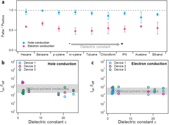
slope extracted from the linear region of the transfer curves. The calculated mobility for both hole conduction and electron conduction branch of three analysed devices before and after depositing solvent molecules are shown in Figure 4 (a). Typical hole and electron mobilities are found to amount to 98.33 ± 5.05 cm2/Vs and 2.30 ± 0.36 cm2/Vs, respectively. We have also calculated the ratio of both hole and electron mobility after and before physisorption of solvent, which is denoted as 𝜇UV-+B/ 𝜇W+V<B+ in Figure 4
(a). We have found a decrease in both hole and electron mobility with all 𝜇UV-+B/ 𝜇W+V<B+ smaller than 1. The overall degradation of charge carrier mobility might be attributed to the introduction of charge impurity by solvent molecules that enhanced
scattering effect. Thus, the motion of charge carriers are hindered.[26] Hole mobility is less affected, with 𝜇UV-+B/ 𝜇W+V<B+ amounting to 0.81 in acetone and 0.98 in benzene. The electron mobility decreased sharply, with 𝜇UV-+B/ 𝜇W+V<B+ spanning from 0.48 for m-xylene to 0.66 for benzene. This contrast originates from different carrier transport mechanisms in holes and electrons in BP. The hole transport was found to be dominated by phonon scattering and was barely influenced by charge-charge scattering so that the modulation of charge carrier concentration weakly affects the mobility. Conversely, electron mobility was mostly limited by charge-charge scattering, implying that charge impurity introduced from surface functionalization would largely affect the motion of charge carriers. Hence, the physisorption of solvent molecules largely reinforces the scattering effect which prevents the transport of electrons and decreased the electron mobility in a larger extent than hole mobility. [8b,14]
Ion/Ioff ratio is another key indicator for evaluating BP devices, which could be deduced by:
𝐼<X 𝐼<VV =
𝐼KL,FU= 𝐼KL,FZX
where 𝐼KL,FU= and 𝐼KL,FZX represent maximum and minimum value of drain-source current on transfer curve. Figure 4 (b) and (c) displays the Ion/Ioff ratio before and after the deposition of solvent molecules. It reveals that in pristine BP FETs, the Ion/Ioff ratio ranges between 105 to 106 for hole conduction and 104 to 105 for electron conduction for all tested devices. The physisorption of solvent molecules did not affect the Ion/Ioff ratio while stable off current values were monitored, indicating that the bandgap Eg could not
be modified by the limited number of molecules (~1013/cm2) physisorbed onto BP by internal built-in potential.[15] Furthermore, solvent molecules are also observed to yield an enlargement of the hysteresis in the transfer curves due to additional dipolar doping induced by vertical electrical field when the gate voltage is applied Detailed results are shown in Figure S5 in the Supporting Information.
Figure 4. (a) Analysis of hole and electron mobility of BP FET before and after physisorption of
molecules, and Ion/Ioff ratio of (b) hole conduction branch and (c) electron conduction branch of three
BP FETs before and after depositing solvent molecules in the order of increasing dielectric constant. The coloured bands marked with “Without solvent molecules” indicate the typical Ion/Ioff ratio range
To further characterize solvent effects on BP FETs, we explored the change in optical properties of BP upon solvent physisorption. Unlike TMDs whose photoluminescence (PL) spectra could reflect the level of doping by solvent molecules via the quantification of the exciton and trion intensity, photoluminescence of black phosphorus has barely been studied due to their small band-gap in few-layer materials and high exciton anisotropy.[2c,9,16] The complex behavior of excitons and trions made it difficult to quantify the charge density modulation by physisorbed molecules, as shown in Figure
S6. Therefore, we focus mainly on the Raman spectra of few-layer BP which are
regarded as fingerprint to properties of BP.[1b] For the sake of consistency with electrical measurements on BP FETs, all Raman spectra were directly recorded from devices. Pristine and solvent treated BP devices were transferred in a N2 filled spectroscopy holder immediately after each electrical measurement, ensuring the same conditions as for electrical characterizations. The spectra were compared before and after the spin-coating of solvents and were normalized to the silicon peak at 520.3 cm-1. Three Raman modes were detected, as shown in Figure 5 (a) and (b). Among the three modes, in-plane vibration modes B2g and A2g are found to be more inert to surface adsorption than out-of-plane mode A1g in thin BP flakes. A red-shift of the A1g mode was observed in toluene (∆=-1.787 cm-1), benzene (∆=-2.372 cm-1), m-xylene (∆=-0.694 cm-1), as a result of an increase in electron concentration who tends to soften the vibrations. The A1g mode of ethanol (∆=+0.484 cm-1), hexane (∆=+1.851 cm-1), chloroform (∆=+1.138 cm-1), IPA (∆= +1.687 cm-1) undergoes a blue shift, corresponding to the hardening of
BP vibrations by hole doping.[17] The Raman trend in the switch of doping is in accordance to the charge transfer measurements in BP FETs, as shown in Figure 5(c), except for volatile solvents such as acetone and p-xylene due to its low coverage on BP under laser excitation. As for B2g and A2g modes, peak shift has values less than 1 cm-1 for most of the solvents yet still keeps the same trend as A1
g mode, revealing that electron/hole concentration also yields variations the in-plane vibration modes.
Figure 5. Raman spectroscopy of few-layer BP upon physisorption of solvent molecules. (a) and (b)
representative Raman spectra of n-doping (toluene) and p-doping (p-xylene) solvent molecules. The dashed lines highlight the obvious shift in A1g mode. (c) Comparison of the A1g mode shift of
few-layer BP (in blue) before and after physisorption of solvent molecules compared to corresponding charge transfer changes (in red).
CONCLUSIONS
In summary, our electrical and spectroscopic study provided unambiguous evidence of the power of the physisorption of solvent molecules on few-layer black phosphorus to tune their opto-electronic properties via charge transfer and/or dipolar interactions. In particular, our electrical measurement on field-effect transistors demonstrated for the first time that tunable chemical doping can be achieved on black phosphorus using the modest doping brought into play by the physisorption of common solvent molecules. Our results revealed that solvent molecules could not only modulate the charge carrier density up to 1012/cm2, but also affect carrier mobility and Raman shift to a large extent. Our findings are of importance both for fundamental and more applicative investigations since numerous solvents are made of small aromatic molecules, which should therefore not be considered as inert media in the processing, but rather as a potent remote control for tuning the properties of 2D materials and consequent device optimization.
EXPERIMENTAL SECTION
Sample preparation. Few-layer black phosphorus were mechanically exfoliated from
bulk crystal (HQ Graphene) by using the scotch tape method and transferred onto thermally oxidized heavily n-doped silicon substrates (Fraunhofer Institute IPMS, ρSi ~ 0.001 Ω∙cm, tox = 90 nm) in a nitrogen filled glovebox.Their thickness was monitored by optical microscope combined with Raman spectroscopy and Atomic Force Microscopy (AFM). The samples were thermally annealed at 200 °C inside a vacuum
chamber to desorb atmospheric adsorbates. Then, they were no longer exposed to air after the annealing and were characterized only under inert atmosphere (N2-filled glovebox). Anhydrous solvents were opened inside the glovebox. To exclude the dielectric screening caused by environmental changes after depositing solvent molecules, we drop-cast each solvent molecule on few-layer BP, and spin-dried at 2000 RPM for 60 s to guarantee the presence of limited number molecules physisorbed on the surface of the BP. The desorption of solvent molecules was performed by thermal annealing at 200°C under N2 atmosphere.
Device fabrication and electrical characterization. As-exfoliated few-layer BP were
coated with 2 layers of PMMA (Allresist, 600K/ 950K) immediately after exfoliation to avoid air exposure. Top-contact (5 nm Cr/ 40 nm Au) field-effect transistors were fabricated by standard E-beam lithography and lift-off in warm acetone in glovebox. All devices were annealed under vacuum at 200°C overnight to remove absorbents. The characterization of device performance was realized by Keithley 2636A under N2 atmosphere.
Raman spectroscopy. Raman and Photoluminescence spectra were recorded in inert
atmosphere (N2) by Renishaw inVia spectrometer equipped with 532 nm laser in a nitrogen-filled sealed holder (Linkam). Samples were mounted in the glovebox and immediately measured after annealing or after molecule deposition to avoid exposure to
contaminant chemicals. The excitation power was kept below 1 mW to avoid local heating damage effects. The wavenumber (energy) resolution was ~1 meV.
AFM measurement. AFM imaging was carried out by means of a Bruker Dimension
Icon set-up operating in air, in tapping mode, by using tip model TESPA-V2 (tip stiffness: k=42 N/m).
XPS measurements: XPS analyses were performed with a Thermo Scientific K-Alpha
X-ray photoelectron spectrometer operating with a basic chamber pressure of ~10-9 mbar and an Al anode as the X-ray source (x-ray radiation of 1486 eV). Spot sizes of 400 μm and pass energies of 200.00 eV for wide energy scans and 10.00-20.00 eV for scans were used.
Computational details: Density functional theory (DFT) calculations were carried
out within the projector-augmented wave (PAW) scheme, as implemented in the Vienna Ab-Initio Simulation Package (VASP).[18] The generalized gradient approximation of Perdew-Burke-Ernzerhof (GGA-PBE) was used to describe the exchange-correlation potential.[19] Grimme’s semi-empirical DFT-D2 corrections were included to take into account the van der Waals interactions between BP surface and molecules. The kinetic energy cutoff for basis set was chosen at 600 eV.[20] A 5´5´1 supercell model was built and a vacuum of 30 Å thickness along the perpendicular direction was used to avoid any physical interactions between periodic
images. Monkhorst-Pack k-point mesh of 2´2´1 and 4´4´1 were chosen to sample the Brillouin zone for geometry optimizations and self-consistent calculations, respectively.[21] The geometric structure was considered to be converged when the residual force on each atom was less than 1×10⁻³ eV/Å.
AUTHOR INFORMATION
PS and YW conceived and coordinated the work. YW worked on sample preparation, device fabrication, optical and electrical characterization. YW analyzed the data. AS and JC did the modeling work under the supervision of DB. YW wrote the paper with all the authors contributing to the discussion and preparation of the manuscript.
ACKNOWLEDGEMENTS
We are grateful to Dr. Marc-Antoine Stoeckel for enlightening discussions. Device fabrication was carried out in part at the nanotechnology facility eFab (IPCMS, Strasbourg). The authors are thankful to H. Majjad, R. Bernard and S. Siegwald for assistance with microfabrication, as well as Mircea Rastei for AFM measurements. We acknowledge funding from the M-ERA.NET project MODIGLIANI and the We acknowledge funding from the European Commission through the Graphene Flagship Core 2 project (GA-785219), as well as the the Agence Nationale de la Recherche through the Labex projects CSC (ANR-10-LABX-0026 CSC) and NIE (ANR-11-LABX-0058 NIE) within the Investissement d’Avenir program
Chemistry (icFRC). The work in Mons is supported by FNRS/F.R.S. JC and DB are FNRS Research Directors.
REFERENCES
[1] (a) M. Buscema, D. J. Groenendijk, S. I. Blanter, G. A. Steele, H. S. Van Der Zant, A. Castellanos-Gomez, Nano Lett. 2014, 14, 3347; (b) L. Li, Y. Yu, G. J. Ye, Q. Ge, X. Ou, H. Wu, D. Feng, X. H. Chen, Y. Zhang, Nat. Nanotechnol. 2014, 9, 372.
[2] a) G. Long, D. Maryenko, J. Shen, S. Xu, J. Hou, Z. Wu, W. K. Wong, T. Han, J. Lin, Y. Cai, Nano Lett. 2016, 16, 7768; (b) F. Xia, H. Wang, Y. Jia, Nat. Comm. 2014, 5, 4458 ; (c) X. Wang, A. M. Jones, K. L. Seyler, V. Tran, Y. Jia, H. Zhao, H. Wang, L. Yang, X. Xu, F. Xia, Nat. Nanotechnol. 2015, 10, 517. [3] (a) L. Kou, T. Frauenheim, C. Chen, J. Phys. Chem. Lett. 2014, 5, 2675; (b) J. Miao, L. Cai, S. Zhang, J. Nah, J. Yeom, C. Wang, ACS Appl. Mater. Interfaces 2017, 9, 10019; (c) S. Y. Cho, Y. Lee, H. J. Koh, H. Jung, J. S. Kim, H. W. Yoo, J. Kim, H. T. Jung, Adv. Mater. 2016, 28, 7020.
[4] (a) C. Anichini, W. Czepa, D. Pakulski, A. Aliprandi, A. Ciesielski, P. Samorì, Chem. Soc. Rev. 2018,
47, 4860; (b) S. Bertolazzi, M. Gobbi, Y. Zhao, C. Backes, P. Samorì, Chem. Soc. Rev. 2018, 47, 6845.
[5] (a) G. Abellán, V. Lloret, U. Mundloch, M. Marcia, C. Neiss, A. Görling, M. Varela, F. Hauke, A. Hirsch, Angew. Chem. 2016, 128, 14777 ; (b) Y. Du, L. Yang, H. Zhou, D. Y. Peide, IEEE Electron Device
Lett. 2016, 37, 429 ; (c) Y. Jing, Q. Tang, P. He, Z. Zhou, P. Shen, Nanotechnol. 2015, 26, 095201; (d) C.
Wang, D. Niu, B. Liu, S. Wang, X. Wei, Y. Liu, H. Xie, Y. Gao, J. Phys. Chem. C 2017, 121, 18084; (e) G. Abellán, P. Ares, S. Wild, E. Nuin, C. Neiss, D. R. S. Miguel, P. Segovia, C. Gibaja, E. G. Michel, A. Görling, Angew. Chem. 2017, 129, 14581; (f) V. V. Korolkov, I. G. Timokhin, R. Haubrichs, E. F. Smith, L. Yang, S. Yang, N. R. Champness, M. Schröder, P. H. Beton, Nat. Comm. 2017, 8, 1385.
[6] (a) A. N. Abbas, B. Liu, L. Chen, Y. Ma, S. Cong, N. Aroonyadet, M. Köpf, T. Nilges, C. Zhou, ACS
Nano 2015, 9, 5618; (b) C. C. Mayorga‐Martinez, Z. Sofer, M. Pumera, Angew. Chem. Int. Ed. 2015, 54, 14317.
[7] (a) G. Liu, S. Rumyantsev, C. Jiang, M. Shur, A. Balandin, IEEE Electron Device Lett. 2015, 36, 1202; (b) Y. Lin, X. Ling, L. Yu, S. Huang, A. L. Hsu, Y.-H. Lee, J. Kong, M. S. Dresselhaus, T. Palacios, Nano Lett. 2014, 14, 5569; (c) J. Choi, H. Zhang, H. Du, J. H. Choi, ACS Appl. Mater. Interfaces 2016, 8, 8864; (d) N. Mao, Y. Chen, D. Liu, J. Zhang, L. Xie, Small 2013, 9, 1312.
[8] (a) W. Lei, G. Liu, J. Zhang, M. Liu, Chem. Soc. Rev. 2017, 46, 3492. (b) D. Xiang, C. Han, J. Wu, S. Zhong, Y. Liu, J. Lin, X.-A. Zhang, W. P. Hu, B. Özyilmaz, A. C. Neto, Nat. Comm. 2015, 6, 6485.
[9] Y. Wang, A. Slassi, M.-A. Stoeckel, S. Bertolazzi, J. Cornil, D. Beljonne, P. Samorì, J. Phys. Chem.
Lett. 2019, 10, 540.
[10] N. Crivillers, S. Osella, C. Van Dyck, G. M. Lazzerini, D. Cornil, A. Liscio, F. Di Stasio, S. Mian, O. Fenwick, F. Reinders, M. Neuburger, E. Treossi, M. Mayor, V. Palermo, F. Cacialli, J. Cornil, P. Samorì,
Adv. Mater. 2013, 25, 432.
[11] M. Gobbi, E. Orgiu, P. Samorì, Adv. Mater. 2018, 30, 1706103.
[12] A. E. Del Rio Castillo, V. Pellegrini, H. Sun, J. Buha, D. A. Dinh, E. Lago, A. Ansaldo, A. Capasso, L. Manna, F. Bonaccorso, Chem. Mater. 2018, 30, 506.
[13] S. Lin, Y. Chui, Y. Li, S. P. Lau, FlatChem 2017, 2, 15.
[14] S. Kim, G. Lee, J. Kim, ECS J. Solid State Sci. Technol. 2018, 7, Q3065.
[15] C. Han, Z. Hu, L. C. Gomes, Y. Bao, A. Carvalho, S. J. Tan, B. Lei, D. Xiang, J. Wu, D. Qi, Nano Lett. 2017, 17, 4122.
[16] J. Yang, R. Xu, J. Pei, Y. W. Myint, F. Wang, Z. Wang, S. Zhang, Z. Yu, Y. Lu, Light: Sci. Appl. 2015, 4, e312.
[17] D.-H. Kang, M. H. Jeon, S. K. Jang, W.-Y. Choi, K. N. Kim, J. Kim, S. Lee, G. Y. Yeom, J.-H. Park, ACS
Photonics 2017, 4, 1822.
[18] G. Kresse, J. Furthmüller, Physical review B 1996, 54, 11169; G. Kresse, D. Joubert, Phys. Rev. B 1999, 59, 1758.
[19] J. P. Perdew, K. Burke, M. Ernzerhof, Phys. Rev. Lett. 1996, 77, 3865. [20] S. Grimme, J. Comput. Chem. 2006, 27, 1787.