HAL Id: hal-00706889
https://hal.archives-ouvertes.fr/hal-00706889
Submitted on 11 Jun 2012
HAL is a multi-disciplinary open access
archive for the deposit and dissemination of
sci-entific research documents, whether they are
pub-lished or not. The documents may come from
L’archive ouverte pluridisciplinaire HAL, est
destinée au dépôt et à la diffusion de documents
scientifiques de niveau recherche, publiés ou non,
émanant des établissements d’enseignement et de
Sub-wavelength energy concentration with electrically
generated mid-infrared surface plasmons
Adel Bousseksou, Arthur Babuty, Jean-Philippe Tetienne, Ioana Cristina
Moldovan Doyen, Rémy Braive, Grégoire Beaudoin, Isabelle Sagnes, Yannick
de Wilde, Raffaele Colombelli
To cite this version:
Adel Bousseksou, Arthur Babuty, Jean-Philippe Tetienne, Ioana Cristina Moldovan Doyen, Rémy
Braive, et al.. Sub-wavelength energy concentration with electrically generated mid-infrared surface
plasmons. Optics Express, Optical Society of America - OSA Publishing, 2012, 20 (13), pp.13738.
�hal-00706889�
Sub-wavelength energy concentration
with electrically generated mid-infrared
surface plasmons
A. Bousseksou,1,∗A. Babuty,2J-P. Tetienne,1I. Moldovan-Doyen,2 R. Braive,3G. Beaudoin,3I. Sagnes,3
Y. De Wilde,2,4and R. Colombelli1,5
1Institut d’Electronique Fondamentale, Univ. Paris Sud, UMR8622 CNRS, 91405 Orsay,
France
2Institut Langevin, ESPCI ParisTech, CNRS UMR 7587, 75005 Paris, France 3Laboratoire de Photonique et Nanostructures, CNRS UPR20, 91460 Marcoussis, France
4[email protected] 5[email protected]
Abstract: While freely propagating photons cannot be focused below their diffraction limit, surface-plasmon polaritons follow the metallic surface to which they are bound, and can lead to extremely sub-wavelength energy volumes. These properties are lost at long mid-infrared and THz wavelengths where metals behave as quasi-perfect conductors, but can in principle be recovered by artificially tailoring the surface-plasmon dispersion. We demonstrate - in the important mid-infrared range of the electromagnetic spectrum - the generation onto a semiconductor chip of plasmonic excitations which can travel along long distances, on bent paths, to be finally focused into a sub-wavelength volume. The demonstration of these advanced functionalities is supported by full near-field characteriza-tions of the electromagnetic field distribution on the surface of the active plasmonic device.
© 2012 Optical Society of America
OCIS codes: (140.5960) Semiconductor lasers; (230.5750) Resonators; (240.6680) Surface
plasmons.
References and links
1. J.B. Pendry, L. Martin-Moreno, and M. Garcia-Vidal, “Mimicking surface plasmons with structured surfaces,” Science 305, 847–848 (2004).
2. F. J. Garcia de Abajo and J. J. Saenz, “Electromagnetic surface modes in structured perfect-conductor surfaces,” Phys. Rev. Lett. 95, 233901 (2005).
3. D. Martin-Cano, M. L. Nesterov, A. I. Fernandez-Dominguez, F. J. Garcia-Vidal, L. Martin-Moreno, and E. Moreno, “Domino plasmons for subwavelengthterahertz circuitry,” Opt. Express 18, 754–764 (2010). 4. N. Janunts, K. Baghdasaryan, K. Nerkararyan, and B. Hecht, “Excitation and superfocusing of surface plasmon
polaritons on a silver-coated optical fiber tip,” Opt. Commun. 253, 118–124 (2005).
5. V. S. Volkov, J. Gosciniak, S. I. Bozhevolnyi, S. G. Rodrigo, L. Martin-Moreno, and F. J. Garcia-Vidal,“Plasmonic candle: towards efficient nanofocusing with channel plasmon polaritons,” New J. Phys. 11, 113043 (2009).
6. E. Moreno, S. Rodrigo, S. Bozhevolnyi, L. Martin- Moreno, and F. Garcia-Vidal, “Guiding and focusing of electromagnetic fields with wedge plasmon polaritons,” Phys. Rev. Lett. 100, 023901 (2008).
7. D. K. Gramotnev and S. I. Bozhevolnyi, “Plasmonics beyond the diffraction limit,” Nat. Photonics 4, 83–91 (2010).
8. M. I. Stockman, “Nanofocusing of optical energy in tapered plasmonic waveguides,” Phys. Rev. Lett. 93, 137404 (2004).
9. R. J. Walters, R. V. A. van Loon, I. Brunets, J. Schmitz, and A. Polman, “A silicon-based electrical source of surface plasmon polaritons,” Nat. Mater. 9, 21–25 (2010).
10. J. A. Schuller, E. S. Barnard, W. Cai, Y. C. Jun, J. S. White, and M. L. Brongersma, “Plasmonics for extreme light concentration and manipulation,” Nat. Mater. 9, 193–204 (2010).
11. A. P. Hibbins, B. R. Evans, and J. R. Sambles,“Experimental verification of designer surface plasmons,” Science
308, 670–672 (2005).
12. C. R. Williams, S. R. Andrews, S. Maier, A. I. Fernandez-Dominguez, L. Martin-Moreno, and F. J. Garcia-Vidal, “Highly confined guiding of terahertz surface plasmon polaritons on structured metal surfaces,” Nat. Photonics
2, 175–179 (2008).
13. E.M. G. Brock, E. Hendry, and A. P. Hibbins, “Subwavelength lateral confinement of microwave surface waves,” Appl. Phys. Lett. 99, 051108 (2011).
14. W. Zhao, O. M. Eldaiki, R. Yang, and Z. Lu, “Deep subwavelength waveguiding and focusing based on designer surface plasmons,” Opt. Express 18, 21498–21503 (2010).
15. N. Yu, Q. J. Wang, M. A. Kats, J. A. Fan, S. P. Khanna, L. Li, A. G. Davies, E. H. Linfield, and F. Capasso, “Designer spoof surface plasmon structures collimate terahertz laser beams,” Nat. Mater. 9, 730–735 (2010). 16. S. C. Kehr, M. Cebula, O. Mieth, T. Hartartling, J. Seidel, S. Grafstrom, L. M. Eng, S. Winnerl, D. Stehr, and M.
Helm, “Anisotropy contrast in phonon-enhanced apertureless near-field microscopy using a free-electron laser,” Phys. Rev. Lett. 100, 256403 (2010).
17. S. C. Kehr, Y. M. Liu, L. W. Martin, P. Yu, M. Gajek, S.-Y. Yang, C.-H. Yang, M. T. Wenzel, R. Jacob, H.-G. von Ribbeck, M. Helm, X. Zhang, L. M. Eng, and R. Ramesh, “Near-field examination of perovskite-based superlenses and superlens-enhanced probe-object coupling,” Nat. Commun. 2, 249 (2011).
18. H. C. Liu and F. Capasso, Eds. Intersubband Transitions in Quantum Wells: Physics and Device Applications (Academic Press, 1999).
19. J.-P. Tetienne, A. Bousseksou, D. Costantini, R. Colombelli, A. Babuty, I. Moldovan-Doyen, Y. De Wilde, C. Sir-tori, G. Beaudoin, L. Largeau, O. Mauguin, and I. Sagnes, “Injection of midinfrared surface plasmon polaritons with an integrated device,” Appl. Phys. Lett. 97, 211110 (2010).
20. FDTD simulations have been performed with the commercial software package LUMERICAL.
21. Y. De Wilde, F. Formanek, R. Carminati, B. Gralak, P.-A. Lemoine, J.-P. Mulet, K. Joulain, Y. Chen, and J.-J. Greffet, “Thermal radiation scanning tunnelling microscopy,” Nature 444, 740–743 (2006).
22. Y. De Wilde, F. Formanek, and L. Aigouy, “Apertureless near-field scanning optical microscope based on a quartz tuning fork,” Rev. Sci. Instrum. 74, 3889–3891 (2003).
23. V. Moreau, M. Bahriz, R. Colombelli, P. A. Lemoine, Y. De Wilde, L. R. Wilson, and A. B. Krysa, “Direct imaging of a laser mode via midinfrared near-field microscopy,” Appl. Phys. Lett. 90, 201114 (2007). 24. A. Bousseksou, R. Colombelli, A. Babuty, Y. De Wilde, Y. Chassagneux, C. Sirtori, G. Patriarche, G. Beaudoin,
and I. Sagnes, “A semiconductor laser device for the generation of surface-plasmons upon electrical injection,” Opt. Express 17, 9391–9400 (2009).
25. B. Knoll and F. Keilmann, “Enhanced dielectric contrast in scattering-type scanning near-field optical mi-croscopy,” Opt. Commun. 182, 321–328 (2000).
26. A. Cvitkovic, N. Ocelic, and R. Hillenbrand, “Analytical model for quantitative prediction of material contrasts inscattering-type near-field optical microscopy,” Opt. Express 15, 8550–8565 (2007).
27. P. M. Krenz, R.L. Olmon, B. A. Lail, M.B. Raschke, and G. D. Boreman, “Near-field measurement of infrared coplanar strip transmission line attenuation and propagation constants,” Opt. Express 18, 21678–21686 (2010). 28. D. Dey, J. Kohoutek, R.M. Gelfand, A. Bonakdar, and H. Mohseni, “Composite nano-antenna integrated with
quantum cascade laser,” IEEE Photon. Technol. Lett. 22, 1580–1582 (2010).
29. M. Schnell, P. Alonso-Gonzalez, L. Arzubiaga, F. Casanova, L. E. Hueso, A. Chuvilin, and R. Hillen-brand,“Nanofocusing of mid-infrared energy with tapered transmission lines,” Nat. Photonics 5, 283–287 (2011).
1. Introduction
Guiding, focusing and confining long-wavelength radiation with metals requires artificially tai-loring the dispersion of surface-plasmon polaritons (SPPs), which at mid-infrared (mid-IR, 10-100 THz) and THz (1-10 THz) frequencies are barely distinguishable from free photons when they propagate on flat metallic surfaces. Such dispersion engineering can be achieved with a properly designed sub-wavelength metallic patterning [1–3]: the new, artificial disper-sion relation leads to SPPs with larger wavevectors than SPPs on planar surfaces (Fig. 1(a)), and consequently with reduced decay-length in the direction orthogonal to the metal surface. Long infrared SPPs can then be manipulated just as their short-wavelength counterparts.
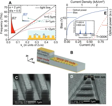
Be-0.0 0.1 0.2 0.3 0.4 0.5 0 10 20 30 40 50 60 70 light line h=0.5μm h=1μm F re q u e n cy (T H z)
kx (in units of 2S/a)
h =2μm a = 2 μm d/a = 0.5 0.000 0.25 0.50 0.75 5 10 Bias Bi a s (V) Current (A) T=300K Optical power O p ti ca l p o w e r (a .u .) 0 1 2
Current Density (kA/cm²)
1275 1300 1325 In te n s it y (A. U .) Wavenumber (cm-1 ) T=300 K I=800 mA E A |E|² |E|² x z y B x z y x z y B C 1μm C 1μm 500 nm D 1μm 500 nm D 500 nm D 1μm
Fig. 1. (a) Dispersion relation of designer’s SPPs for a fixed grating period a=2 µm, d =1 µm and various grating depth h. Bottom inset: schematics of the metal grating and
definition of the geometric parameters. Top inset: Effect of the dispersion relation on the confinement: larger wavevectors yield increased field confinements. (b) Schematics of the device and operating principle. (c,d) Scanning electronic microscope image of the sub-wavelength metal grating (c, cross section) and of the focusing end of the device (d). (e) Voltage-current (solid blue line) and light-current (dashed red line) characteristics at room-temperature of a 1400-µm-long and 22-µm-wide device. Inset: Typical emission spectrum at RT. The measurements are performed in pulsed mode (50 ns pulses, 84 kHz repetition rate), using a Fourier Transform Infrared Spectrometer equipped with a liquid-nitrogen-cooled HgCdTe detector. The laser threshold current density is 1.8 kA/cm2
cause of their spectral location, THz and mid-IR plasmonics promise to lead to a variety of applications in detection and bio-detection [4]. Crucial to this goal, is the availability of an enabling technology which can (i) generate SPPs on demand, at room temperature and with reasonable power, (ii) guide the radiation on a chip, (iii) over distances much larger than the wavelength, and (iv) concentrate the electromagnetic (EM) field within micron-scale-distances of the surface. Such a result will also open the way to the development of active tools for near-field microscopy in a difficult spectral range, where fibers are not available [5]. The goal of this letter is to demonstrate this enabling concept.
At near-infrared wavelengths, functionalities such as guiding and energy focusing, us-ing tips or wedge/channel SPP waveguides have been proposed and demonstrated [6–8]. Semiconductor-based generation is reported in [9], and a complete review can be found in [10]. At longer wavelengths, possibly because of the increased difficulty in generation and detection of SPPs, few experimental demonstrations are present [11–14]. These works have however val-idated the concept of designer SPPs at microwaves and sub-THz frequencies on passive metal structures [3]. Designer SPPs structures on the highly doped semiconductor facets of THz quan-tum cascade lasers have also been used to collimate the laser beam output [15]. We demonstrate
here a device, which operates at room temperature, is electrically driven and is able to generate, couple, propagate with sub-wavelength confinement on a chip (over macroscopic distances), and focus mid-IR radiation into a sub-wavelength region. We employ a scattering near-field scanning optical microscope (s-NSOM) to directly elucidate the SPP presence, propagation and characteristics, and demonstrate sub-wavelength confined guiding and focusing effects. Note that we provide s-NSOM measurements as a function of the tip-to-surface distance too. This is rarely seen at long IR wavelengths [16, 17], but it is crucial to prove that the EM field is confined within sub-wavelength proximity of the artificially patterned metallic surface in all three dimensions of space.
2. Design and fabrication
Figure 1(a) shows the calculated dispersion relation of designer SPPs propagating along a prop-erly structured gold surface, whose schematics is reported in the inset. At constant frequency, increasing the grooves depth increases the in-plane (kx) wavevector [1–3]. The SPP electric
field decay length -δz = √ 1 k2
x−k20
where k0 is the free-photon wavevector- is also decreased,
and the EM field is enhanced close to the interface. Increasing the wavevector increases the propagation (ohmic) losses. The energy attenuation length isα1x=2Im1(kx).
Given a target frequency of 40 THz (our laser emits at λ≈7.7 µm) a grating with geometrical parameters d= 1 µm, h = 0.7 µm and a = 2 µm is a good trade-off between confinement (δz=
3.08µm) and loss (1/αx = 115 µm). These are the parameters used for the device presented
in this paper , whose scheme is presented in Fig. 1(b). It is based on a mid-IR quantum cascade laser (QCL) emitting at (λ≈7.7 µm), whose details can be found in the Appendix 1.
We exploit the transverse magnetic (TM) polarized emission, a natural feature of QCLs [18], to directly couple the output laser radiation into a SPP mode [19]. The sub-wavelength grating is patterned into a silicon dioxide (SiO2) carrier layer and it starts in the near-field (1-2 µm
distance) of the laser output facet, which corresponds to the end-fire coupling geometry. The top and sides of the patterned SiO2grating are then coated with gold, as shown in Figs. 1(c)
and 1(d). This grating can be seen as a practical realization of the recently proposed domino plasmons geometry [3,13]. The laser output is hence coupled into the SPP modes on the gold/air interface.
3. Far-field and near-field analysis
Figure 1(e) presents the optoelectronic characterization of the laser source, as measured at room temperature (300K) as a function of the injected current. The corresponding laser spectrum is shown in the inset of Fig. 1(e).
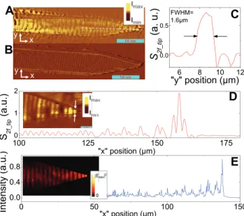
The grating is designed in a geometry which is meant to focus the SPPs at its end tip, which is located on the opposite end with respect to the laser output facet. The focusing grating is constituted of two main parts (see Fig. 2(b) for the AFM topography). The first section (180-µm-long in the x-direction) has a fixed width (40-µm-wide in the y-direction). It is twice as wide as the laser ridge waveguide, to ensure maximum coupling between the laser and the SPP carrying layer. Using finite difference time domain (FDTD) simulations [20] we estimate a coupling efficiency∼ 30%. The second part (80-µm-long in the x-direction) of the focusing grating is a two dimensional funnel: it is 40-µm-wide at the beginning and 500 nm-wide at the tip. Scanning electron microscopy (SEM) images of the focusing grating and of the tip are shown in Figs. 1(c) and 1(d). We have employed a custom-built mid-IR s-NSOM [21,22] to map the near-field on the grating surface. Our previous works on QCLs [23, 24] have demonstrated that s-NSOM is a powerful and robust technique, which yields simultaneously the topography and the near-field signals. Figures 2(a) and 2(b) show a wide two dimensional scan (250 µm x 70
100 125 150 175 0 1 2 S 2 f_ ti p (a .u .) "x" position (μm) 6 8 10 12 0.0 0.5 S 2 f_ ti p (a . u .) "y" position (μm) FWHM= 1.6μm 0 50 100 150 0.0 0.4 0.8 In te n s it y (a .u .) "x" position (μm)
C
D
A
E
x y x yB
Fig. 2. (a,b) Near-field optical signal demodulated at the second harmonic frequency of the tip, S2 f tip, and AFM topography of the focusing grating device. The s-NSOM is operated
with a tungsten tip oscillating at a frequency ftipwith amplitude 100 nm. (c) 1D
cross-section of the near-field signal performed at the funnel end along the y axis, as highlighted by the white dotted arrows in the inset of Fig. 2(d). (d) 1D cross section of the near-field signal performed along the x-axis following approximately the dashed white line in Fig. 1(a). The signal at the funnel-end (right side of the figure) is on average 5 times more intense than on the funnel beginning. Inset: Close-up of the s-NSOM image around the funnel-end of the focusing grating. (e) Finite element 3D calculation of the focusing grating device. The image in the inset shows the electric field intensity (|Enorm|2) recorded at a
distance of 0.1 µm above the sub-wavelength grating. The main figure shows a 1D cross section for comparison with the data in panel d, showing a good qualitative agreement.
µm) of the sub-wavelength focusing device. The near-field signal (Fig. 2(a)) proves that the EM field follows the metallic waveguide and it is confined onto the sub wavelength grating. Note that the near-field signal is detected here at twice the tip oscillation frequency using a lock-in amplifier, and is therefore denoted as S2 f tip, in order to suppress any possible contribution from
background scattering [25,26]. Its intensity globally decays along the propagation direction (the x-direction) in the initial, constant-width section of the grating. An estimate of the SPP decay length (1/αx) is provided in Appendix 3. We obtain 60 µm, while the theoretical estimate is 115
µm. We attribute the difference to processing imperfections (roughness of the metallization), which reduce the propagation length. This estimate is based on the assumption that the field intensity distribution along z does not change significantly as the grating becomes narrower. This hypothesis is supported by theoretical calculations - reported in [3] - showing that the dispersion relation in a designer’s plasmons waveguide is independent of the grating width, even when the latter becomes narrower than the wavelength.
The decay length we experimentally measure is 10 times larger than what can be obtained with strip transmission lines [27], thus enabling on-chip mid-IR circuitry. Note: the vertical confinement reported in Refs. [27, 29] is tighter, but the confinement achieved here is sufficient for our scope, which is to guide and focus mid-IR radiation into sub-wavelength volumes. A legitimate question is, however, the comparison of the two approaches at equal field confine-ments. We have theoretically compared the microstrip lines in [27] with a modified design
based on designer’s SPPs, featuring an intensity perpendicular confinement of 700 nm. The corresponding calculated propagation length is∼ 83 µm (∼ 10 × λ), while a microstrip line -according to [27] - would yield a value of∼ 12µm, i.e. of the order of the wavelength.
In the second, funnel-like section of the grating the trend is reversed: the focusing effect overcomes the losses, a gradual field enhancement along the propagation direction is detected, and a maximum intensity is measured at the funnel tip (Fig. 2(d) and inset). Figures 2(c) and 2(d) show 1D cross sections (y- and x-directions, respectively) of the near-field measurements in Fig. 2(a).
A minimum field enhancement by a factor of 5 at the funnel-end with respect to the aver-aged field intensity at the funnel beginning, and also a sub-wavelength (1.6 µm) measured full width at half maximum (λ/5) confinement along the y direction at the tip end are demonstrated. The measurements are in good agreement with our FEM (finite element method) simulations, reported in Fig. 2(e) and inset. This is the first demonstration of surface-wave generation, prop-agation, focusing and sub-wavelength field confinement combined in a single device operating at room temperature and with good performances. Note that these functionalities are spatially separated (our structure is approximately 40 times λ long), since a propagating surface wave is focused. This is in contrast with antenna focusing which leads to higher spatial confine-ments [28, 29], but requires in general wavelength-sized objects which are entirely immersed in the radiation incoming from free space. Additional functionalities, such as waveguide bends, which are essential for lab-on-chip applications, can be implemented within the same approach, and are described in Appendix 2.
4. Evidence of field-enhancement with designer’s surface-plasmons
In the last part of the paper, we present evidence of the increased perpendicular field confine-ment of the designer’s SPPs, a consequence of the artificially engineered dispersion (see Fig. 1(a)). The tip oscillates along z, with an oscillation amplitude of α≈ 100 nm and with an oscillation frequency ftip= 32 kHz. In order to get some insight regarding how far the
elec-tromagnetic field extends above the metallic grating, the s-NSOM tip - at a given position on the device surface - is retracted from the z= z0position (tip in contact with the grating) to the z= z0+ 10 µm position. The s-NSOM signal S at the optical detector is demodulated with a
lock-in amplifier at the laser frequency rate flaser= 85 kHz. The measurement of S at flaser,
which we call Sflaser, allows one to detect the presence of the electromagnetic field at large distance from the surface when the tip apex is far from its image.
This is not possible when demodulating the s-NSOM signal at ftip(first or second harmonic)
[25, 26]. A simple Taylor expansion of S(z + α cos 2π ftipt) about z shows that for small α, the
demodulated signal at ftip(or 2ftip) is proportional to the first (or second) derivative of σ|E|2
with respect to z. For the devices investigated in the paper, the field E varies on a scale of several micrometers (metal grating) or of several tens of micrometers (flat metal surface), which is in both cases much larger than α. Within a few hundreds of nanometers from the sample surface, the variations of E with respect to|z0-z| on the scale of α are therefore negligibly small in
comparison to the strong variations of σ induced by the image of the tip in the sample surface. To a first approximation, the signal demodulated at ftipis then proportional to|E|2 dσdz, and the
signal demodulated at 2ftipis proportional to|E|2 d
2σ
d2z. At larger tip-sample separation,σ = σ0
and detection at ftipor 2 ftip, yields to a signal proportional σ0d|E|
2
dz or σ0 d2|E|2
d2z .
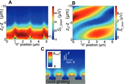
Note that Sflaser results from scattering of the electromagnetic field by the entire tip structure, and not only from the tip apex, which only allows one to obtain a qualitative insight regarding the field confinement. We have measured Sflaser versus the tip-sample distance|z−z0| at various ”x” positions along a line crossing the metallic grating to scan the near-field in the x-z plane.
C B Sf_ la se r (μ V) z0 -z (μ m) A Sf_ la se r (μ V) z0 -z (μ m) z0
Fig. 3. (a,b) Near-field optical signal demodulated with a lock-in amplifier at the laser modulation frequency, Sf laser. The scattered near-field signal is measured as a function of
the x-z tip position, while the y position is fixed. z0is the absolute z coordinate (measured at
each x position) corresponding to the situation where the tip is in contact with the sample surface. Hence,|z- z0| is the distance between the tip and the sample surface. The color
map intensity is in µV (micro-Volts) and it corresponds to the lock-in amplifier signal. Panel (a) reports the measurements on the sub-wavelength grating. The solid black line is the simultaneously acquired grating profile obtained by measuring z0 as a function of x.
Panel (b) reports the measurements on a metallic unpatterned section of a reference device. The measurements are performed with the same tip and at identical laser injection currents. (c) Finite-elements numerical simulations of the electric field intensity|Enorm|2on the
sub-wavelength grating. The geometric and sub-wavelength parameters are in agreement with the measured device shown in Fig. 3(a).
This measurement is possible as little stray photons are present on the device and the majority of the field is evanescent. The result of this scan is shown in Figure 3.
We compared the s-NSOM signal Sflaser on the sub-wavelength grating with a reference de-vice where SPPs are injected onto a plain, un-patterned metallic guide at the output facet of an identical QCL, processed simultaneously on the same chip. The same injection current was used on both devices to allow a proper comparison. The measurements (Fig. 3(a)) in the sub-wavelength metal grating show clear field confinement close to the surface. Indeed, Sflaser de-cays over a distance of the order of 3 µm, which indicates that there is no significant field associated to the spoof SPPs beyond this distance from the grating. This behavior agrees qual-itatively with the theoretical value of the field intensity decay length which is predicted to be ≈ 1.5 µm (see Fig. 3(c)).
Note that the measurements of Sflaser in Fig. 3(a) start in contact with the surface (at |z-z0|=0), while z0 shown by the black solid line varies sometimes abruptly with x as it follows
the grating profile, which produces apparent discontinuities in the figure. The data prove that little field is present at more than 3 µm from the metallic surface: indeed the designer SPPs are tightly bound to the metallic layer. Furthermore, this measurement excludes the presence of a significant background originating from the laser source, which is also supported by the fact that NSOM images recorded in the xy plane on the sub-wavelength grating at ftipand 2 ftipare
essentially identical (data not shown). On the contrary, the reference device yields a signal over the entire range which is accessible with the s-NSOM in the z-direction, as in Fig. 3(b). This is consistent with the poor confinement (δz /2= 27 µm) expected for a SPP on a flat surface
in the mid-IR. The patterned metallic surface induces a (sub-wavelength) field confinement one order of magnitude higher than a flat surface. Note: the absolute value of the s-NSOM signal demodulated at flaseris much larger on the metal grating than on the unpatterned metallic
surface. This is a first indication that the enhanced confinement of the designer’s plasmons leads to an enhanced EM field at the metal-air interface. By comparing the magnitude of the near-field signals detected with the same tip at twice its oscillation frequency on the two devices, we estimate that the intensity of the surface EM field of designer SPPs is about one order of magnitude larger than for regular SPPs.
5. Conclusions
In conclusion, we have demonstrated the generation, sub-wavelength confined guiding over macroscopic distances and sub-wavelength concentration of mid-IR energy with an electrically-powered and room-temperature operating device. Besides the obvious advantage of being com-pact, the demonstrated concept opens new vistas for integrated plasmonics at long-IR wave-lengths, since it uses propagating waves which are at the same time highly confined. Further-more, it is possible to couple this architecture with plasmonic antennas, tapered transmission lines, and/or metallic nano-particles.
Appendix 1: Laser material and device processing
The samples were grown in a vertical-reactor, low-pressure MOVPE system using hydrogen as carrier gas and standard precursors (arsine (AsH3), phosphine (PH3), trimethylindium (TMI), trimethylgallium (TMGa) and trimethylaluminium (TMAl)). Our growth conditions lead to an InGaAs and an InAlAs growth rate of around 1.8 ML/s for the active region.
The sample is grown on a low-doped (n ≈1017cm−3)InP substrate. The
ac-tive region contains 50 repeats of the following 4-well active region+injector
structure (beginning with the injection barrier, layer thicknesses in nm):
4.3/1.7/1.0/5.3/1.2/5.2/1.2/4.4/2.5/3.1/1.7/2.9/1.6/2.7/1.8/2.6/2.1/2.6/2.4/2.4 where bold numbers refer to Al0.52In0.48As barriers, roman type to In0.53Ga0.47As wells, and the under-lined layers are n-doped to 1x1017cm−3. The stack of active regions+injectors is sandwiched between top and bottom 0.5-µm-thick n-doped 5x1016 cm−3 InGaAs layer. The growth is then followed by a 3.35-µm-thick InP top cladding layers (2.5 µm n-doped 5x1016cm−3 and 0.85-µm n-doped 5x1018cm−3) and finally an InGaAs 0.1-µm-thick contact layer (n-doped 9x10¹⁸).
Standard laser ridges (22 µm wide, 1.5 mm long and 7.5 µm deep) were defined using in-ductively coupled plasma (ICP) etching. The whole sample was then passivated with a 700 nm-thick SiO2layer, which was etched on top of the laser ridges to allow electrical contacts.
The same layer was also shaped - using electron-beam lithography followed by reactive ion etching - into bent and/or tapered sub-wavelength gratings at the proper positions on the sam-ple. A Ti/Au metallization (5/200 nm thick) was evaporated at tilted angles, to provide both the electrical contact on top of the laser ridges, and the SPP carrying layer. After polishing and back-contact deposition, the samples were cleaved and In-soldered onto copper blocks for characterizations.
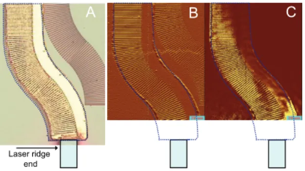
Appendix 2: Curvilinear Devices
Figure 4 shows an optical microscope image of our curved waveguide device. It is composed by two circular - in opposite directions- successive bends of 45 degrees. The waveguide is 40 µm wide, and the radius of curvature of the two bends is∼100 µm. The geometry of the sub-wavelength grating is identical to the focusing devices presented in the main core text of the paper. For processing reasons we have fabricated an identical, spatially translated reference curved waveguide which is however kept without metallization layer.
C B
A
Laser ridge end
Fig. 4. Miscroscope (left), topographic (center) and NSOM (right) images of a typical curvilinear device.
The two right panels of Fig. 4 show the topographic image (center) and the s-NSOM image (right) measurements on the curved waveguide. The measurements show a clear guiding effect of our designer’s SPPs in the circularly shaped waveguide. Note that the near-field signal is localized exclusively onto the metal coated sub-wavelength grating and it does not follow the non-patterned metallic region.
Appendix 3: Estimate of SPP decay length
The plasmonic waveguides used in this first demonstration are 40 µm wide in the Y direction: they can therefore support several transverse modes. Figure 5 shows an X-section of a 3D numerical simulation of the eigenmodes of such a waveguide: higher order modes are multi-lobed along the Y-axis.
M1 M2 M3 M5 M4 0 |Emax|²
Fig. 5. Cross-section of the field-distribution (squared norm of the electric field) for 5 trans-verse modes sustained by the plasmonic waveguide.
If several modes are simultaneously present (multimode case), the value of the extracted de-cay length can depend on the chosen Y-section. We have therefore experimentally extracted the decay length value from a device with a uniform-width designer SPP waveguide and sustaining only one mode, as shown in Fig. 6.
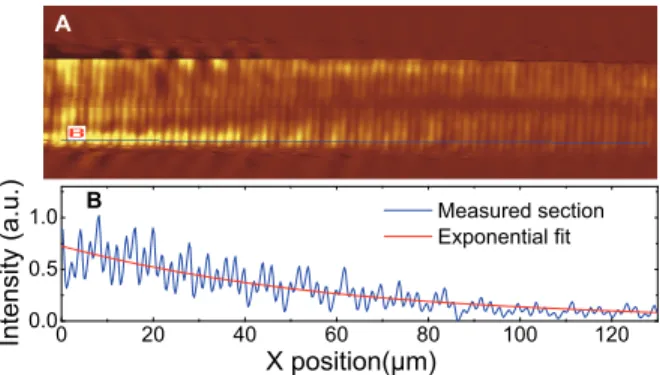
A B 0 20 40 60 80 100 120 0.0 0.5 1.0 Measured section Exponential fit In te n si ty (a .u .) X position(μm)
Fig. 6. (A) NSOM image of a stright plasmonic waveguide with only one transverse mode propagating. (B) 1D cross section of the NSOM signal, and exponential fit of the decay length
The NSOM measurements are performed in a ”constant-width” section of a 40 µm-wide de-signer’s SPPs waveguide. This device and the one presented in Fig. 1 of the paper are located on the same semiconductor chip. As shown in Fig. 6, the propagating mode exhibits two lobes (second transverse mode according to Fig. 5). Assuming that one transverse mode only is prop-agating along the plasmonic waveguide, we extract a decay length of∼ 60 µm. Our goal here is to provide a lower limit for the propagation losses for comparison with existing works (tapered transmission lines, for instance).
Acknowledgments
We acknowledge financial support from the French National Research Agency (ANR-07-NANO-039 ”NanoFtir” and ANR-09-NANO-020 ”Gospel”), the RTRA project “PHLARE”, and from the Centre de Comp´etences Nanosciences Ile-de-France (PSTS). The device fabrica-tion has been performed at the nano-center CTU-IEF-Minerve, which was partially funded by the Conseil G´en´eral de l’Essonne.