HAL Id: hal-02109964
https://hal.sorbonne-universite.fr/hal-02109964
Submitted on 25 Apr 2019HAL is a multi-disciplinary open access archive for the deposit and dissemination of sci-entific research documents, whether they are pub-lished or not. The documents may come from teaching and research institutions in France or abroad, or from public or private research centers.
L’archive ouverte pluridisciplinaire HAL, est destinée au dépôt et à la diffusion de documents scientifiques de niveau recherche, publiés ou non, émanant des établissements d’enseignement et de recherche français ou étrangers, des laboratoires publics ou privés.
Evolutionary Optimization of All-Dielectric Magnetic
Nanoantennas
Nicolas Bonod, Sébastien Bidault, Geoffrey Burr, Mathieu Mivelle
To cite this version:
Nicolas Bonod, Sébastien Bidault, Geoffrey Burr, Mathieu Mivelle. Evolutionary Optimization of All-Dielectric Magnetic Nanoantennas. Advanced Optical Materials, Wiley, 2019, pp.1900121. �10.1002/adom.201900121�. �hal-02109964�
Evolutionary Optimization of All-Dielectric Magnetic
Nanoantennas
Nicolas Bonod, Sébastien Bidault, Geoffrey W. Burr, and Mathieu Mivelle* Dr Mathieu Mivelle
Sorbonne Université, CNRS, Institut des NanoSciences de Paris, UMR 7588 4 place Jussieu, tour 22, 22-32, 505, 75005 Paris, France
Email: [email protected] Dr Nicolas Bonod
Aix Marseille Univ, CNRS, Centrale Marseille, Institut Fresnel, 13013 Marseille, France Dr Sébastien Bidault
Institut Langevin, ESPCI Paris, PSL University, CNRS, 75005 Paris, France Dr Geoffrey Burr
IBM Almaden Research Center, San Jose, California 95120, United States
Keywords: Dielectric nanoantennas, magnetic light, evolutionary algorithm, inverse design, light-matter interactions, nanophotonics
Abstract
Magnetic-light and matter interactions are generally too weak to be detected, studied and applied technologically. However, if one can increase the magnetic power density of light by several orders of magnitude, the coupling between magnetic-light and matter could become of the same order of magnitude as the coupling with its electric counterpart. For that purpose, photonic nanoantennas, in particular dielectric, have been proposed to engineer strong local magnetic field and therefore increase the
physical limitations that confine the magnetic hot spot in the core of the material itself, preventing experimental and technological implementations. Here, we demonstrate that evolutionary algorithms can overcome such limitations by designing new dielectric photonic nanoantennas, able to increase and extract the optical magnetic field from high refractive index materials. We also demonstrate that the magnetic power density in an evolutionary optimized dielectric nanostructure can be increased by a factor 5 compared to state-of-the-art dielectric nanoantennas and that the fine details of the nanostructure are not critical in reaching these aforementioned features, as long as the general shape of the motif is maintained. This advocates for the feasibility of nanofabricating the optimized antennas experimentally and their subsequent application.
1. Introduction
Light and matter interactions are often considered to be mediated by the optical electric field only, neglecting its magnetic counterpart.[1] This is particularly true in
quantum optics, where the electric field couples much more strongly to the electric dipole of a quantum emitter than the magnetic field with the magnetic dipole (at least two orders of magnitude).[2-5] Nevertheless, increasing the magnetic energy density of
light was by several orders of magnitude with respect to the electric one would be counterbalance the predominance of electric light-matter interactions. The potentiated occurrence of magnetic light and matter interactions would open up a new scope of possible applications in a variety of fields such as optoelectronics, nonlinear and nano-optics, spintronics, metamaterials, chiral nano-optics,[6] sensing,[7] and photochemistry[8]. After
experimental demonstrations of the coupling between magnetic dipolar emitters and non-resonant photonic structures,[9-15] both dielectric[5,16-30] and plasmonic[29,31-36]
optical nanoantennas were recently proposed to boost the magnetic field of light in several theoretical studies. Along the same lines, some of these structures were theoretically shown to strongly increase the emission rates of magnetic dipoles.[5,19,21,24,25,27,28,32,34,37] In fact, experimental evidence for the capacity of optical nanoantennas to manipulate the emission of such dipoles at visible [38-42] or
near-infrared[43] wavelengths has been brought about recently. In that context, based on Mie
resonances, high index dielectric nanoparticles are of particular interest to efficiently enhance the magnetic optical field at visible wavelengths through strong displacement currents taking place inside these nanoantennas.[25] However, current antenna designs
suffer from the fact that the magnetic enhancement occurs inside the material, in the core of the structures, making it difficult to access the hotspot experimentally and use its full potential.[44] Hollow nano-disks[24,27,28] (i.e nanocylinders) were proposed to
overcome this hurdle, granting access to the magnetic field that would be partially enhanced in air and not entirely in the dielectric material. We recently used this approach to experimentally couple such structures to magnetic emitters, demonstrating the manipulation of the magnetic local density of states.[40] However, it is still very
challenging to place a nanoscale piece of material inside hollow nanodisks, making nanostructures featuring easily accessible magnetic hotspots particularly appealing. Along those lines, it was recently demonstrated that evolutionary algorithms[45] can
produce optical nanostructures behaving far better than conventional photonic antennas[46-48] or devices.[49-53] By coupling the power of computation algorithms to
specific goals and the intuition of researchers, these approaches are redefining what might be the future of nanophotonics.[45]
In this paper, we demonstrate that evolutionary algorithms are a powerful alternative to design dielectric optical nanostructures able to strongly enhance the optical magnetic field of light at visible wavelengths, in the near field. Furthermore, while dielectric nanoantennas usually create a magnetic field hotspot inside the material (i.e. inside the antenna), the architectures developed here feature a reachable magnetic field just above the antenna, with up to 5 times more enhancement than hollow nanodisks. We finally show that, although algorithmically optimized geometries are more elaborate than the shape of conventional nanoantennas, their photonic response depends very weakly on the fine details of the design. In fact, a rough fabrication process following the general shape of the optimized antenna would still lead to more than a 4 times enhancement of the optical magnetic intensity with respect to state-of-the-art nanoantennas, highlighting the feasibility of their experimental implementation.
2. Results
2.1. Description of the Genetic Algorithm
Numerical evolutionary algorithm techniques mimic the natural selection processes that happen during the evolution of species. Figure 1a summarizes this approach for the design of silicon-based nanoantennas featuring enhanced magnetic fields. First, a population of random nanostructures is generated. Then, each population is evaluated for our specific goal through Finite Difference Time Domain (FDTD) simulations, in
order to obtain the highest optical magnetic intensity at a targeted location in the near field of the nanostructure. From this analysis, we select the antennas that provide the best results and we create a new population by either mutationing or breeding these selected designs. This second generation is then evaluated again through FDTD, and so on until, after several generations, an optimized solution emerges. In here, each population is composed of 20 elements and each new generation is elaborated from the 5 best structures favored during the selection process (see supporting information). Each element of each generation is reduced to a 11x11 binary matrix made of 0 and 1,[46] as shown in Figure 1b, and each 1 of this matrix corresponds to a parallelepiped made of silicon in the FDTD simulation, while each 0 corresponds to air. The center of these silicon blocks is then placed in an array with a periodicity of 30 nm in x and y inside the FDTD simulation. At first, the x and y dimensions of the silicon parallelepipeds are set to 40x40 nm2, a dimension slightly larger than the periodicity in order to have overlapping blocks of silicon at certain places, allowing displacement currents to emerge inside the dielectric material of the antenna. An example of the corresponding structure associated to the matrix in Figure 1b is displayed in Figure 1c. The full width D in Figure 1c was set to 340 nm. The thickness h of the structure was 110 nm (Figure 1d), in order to ensure a π phase shift of the incoming plane wave between the entrance (lower part) and the exit (top part) of the silicon elements (for an optical index of the silicon obtained experimentally[40]). This condition is usually required for dielectric Mie resonators used to enhance the magnetic optical field[44],
which led us to use it as a starting point in the simulations. The nanostructure was illuminated in normal incidence by a plane wave, 600 nm in wavelength and circularly
polarized. The maximization of the magnetic intensity was then investigated just above (in the first mesh cell in z), and in the centre (x,y) of the structure (red spot in Figure 1c and d).
The FDTD method is time consuming and requires high computational power. Therefore, in order to speed up the selection process, we first used a rough discretization mesh of 10x10x10 nm3 in size to describe the binary matrices in the simulations. For the same purpose of saving computation time, the simulations were stopped after 10 optical cycles, a number that is sufficient to reach a plateau in the optical response of the simulated nanostructures.
Figure 1. General concept of the genetic algorithm (GA) developed for designing nanostructures that optimize local magnetic fields. a) Schematic of the different steps realized during the selection process. First, a random generation of 20 elements is created, an each of these elements is evaluated through Finite Difference Time Domain (FDTD) simulations. The 5 structures giving the highest magnetic field intensity are selected and 20 new elements are created by either mutating or breeding the 5 selected elements. This new generation is then evaluated through FDTD again until, after several generations, an optimized solution emerges. b) Typical binary matrix defining a structure to be evaluated: each 1 corresponds to a silicon parallelepiped in the FDTD simulation. c) Schematic representation, in the (x,y) plane, of the structure produced by the matrix in b), (D = 330 nm). d) Cross section of the structure in c, in a (x,z) plane (indicated by the dashed line in c), (h = 110 nm). The nanostructures are
excited by a plane wave, at λ=600 nm, with a circular polarization and propagating in a direction normal to the (x,y) plane. The red spot in c and d corresponds to the position where the magnetic intensity enhancement is evaluated (the first mesh cell above the structure).
2.2. Genetic Optimization of a Dielectric Antenna
Taking into account all these parameters, figure 2a displays the typical optical magnetic field intensity enhancement in the center (x=y=D/2, z=h+5 nm) of the generated structures during the evolutionary process. In here, each data point represents a single simulation of a unique nanostructure. Each generation is therefore composed of 20 data points, meaning that more than 7000 independent simulations are presented in figure 2a. As we can see, the magnetic field intensity enhancement quickly increases with the number of generations, reaching a plateau after about 150 successive mutations of the nanostructure geometry. Figures 2b and d show 2 structures at different steps of the evolutionary process, at respectively generation 50 and 100. We observe that the central shape is maintained already from a very early point onwards in the selection process, suggesting an important role in the magnetic field intensity enhancement. In addition, figures 2c and e display the magnetic field intensity enhancement of the structures presented in figures 2b and d, respectively. We notice that the magnetic intensity distributions are rather similar in shape but with a higher confinement and enhancement in the case of generation 100, indicating that the changes at the periphery of the structure from
generation 50 to 100 resulted in a high concentration of the magnetic energy density and therefore to a higher intensity enhancement.
Figure 2. Magnetic field intensity enhancement during the evolutionary process. a) Number of generations M a g n e ti c I n te n s it y E n h a n c e m e n t 0 6 12 0 6 12 18 a b c d e Generation 50 Generation 100 100 nm 248 IHI2/IH0I2 IHI2/IH0I2
1c and d) versus the number of generations. Each generation displays the results of 20 structures (20 data points), characterizing the extending increase of the magnetic intensity for each generation. b) Optimal structure at generation 50 and c) corresponding magnetic intensity enhancement distribution in a plane 5 nm above the silicon (z=115nm). d), e) Optimal structure and distribution of the magnetic field intensity increase, in the same plane as c), at generation 100.
2.3. Behavior of the Optimized Antenna
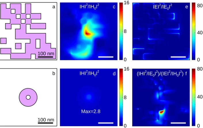
From figure 2a, we were also able to identify the design with the highest magnetic field enhancement selected by the algorithm, which was found to be at generation 248 and is presented in figure 3a. In order to better describe the behavior of that specific structure, the mesh of the simulation was then changed to 2x2x2 nm3 and a second
optimization allowed by this fine mesh was performed, consisting in changing the aspect ratio (global size of the antenna), the thickness and the sizes of the parallelepipeds made of silicon (see supporting information). The final structure was then found to be made of parallelepipeds of silicon with dimensions of 36x36 nm2 in
(x,y) and 92 nm in z, surrounded by air and positioned with a periodicity of 33 nm in x and y, with a total width D of 366 nm. This nanostructure was then compared, in the same conditions and using the same materials, to a hollow nanodisk,[24,28] the best
silicon nanoantenna known so far with both high enhancement and good accessibility of the field.
Figures 3c and d display the magnetic intensity enhancement 2nm above the GA design and the hollow nanodisk, respectively. Although the reduction of the mesh size slightly lowers the magnetic field intensity enhancement, we can see that the GA reaches a magnetic energy density that is five times higher than that of the hollow nanodisk, demonstrating the potential of evolutionary algorithms to generate accessible hot spots of the magnetic field only. A similar comparison can be performed between the genetically optimized antenna and other commonly used dielectric resonators for enhanced magnetic fields such as a single silicon disk or a dimer of Si disks (see figure S5). Importantly, the magnetic field intensity enhancements simulated here for a disk dimer and a hollow nanodisk are in good agreement with recently reported experimental values [40-41], validating the relevance of the comparison made
here. These simulations indicate that the GA design offers a very significant enhancement of the magnetic field intensity above the antenna that is 10x and 8x larger than for a single disk or a dimer, respectively.
Apart from the magnetic enhancement, the ratio between the magnetic and electric field intensity is also an important feature for an effective magnetic antenna. Figures 3e and f display the normalized electric field intensity and the ratio between magnetic and electric normalized intensities, respectively, in the same plane as figure 3c. From these figures, we see that the electric and magnetic field do not overlap in the near field of our GA design. In addition, we can observe that, at certain positions, the ratio of magnetic over electric intensities is very high (more than 80). Although being not the main focus of this paper, it is worth noticing that such a genetic algorithm could
equally be used to optimize this relative magnetic / electric ratio instead of optimizing the magnetic field enhancement. This would be of particular interest to specifically study the coupling between magnetic light and matter with a very high efficiency and without competition from the electric optical field.
Figure 3. Optimized structure and comparison with a hollow silicon nanodisk. a) Optimized structure obtained after 248 generations and c) distribution of the magnetic intensity enhancement a) 2nm above the top plane of the antenna in z. b) Schematic of a silicon hollow nanodisk, currently considered as the best dielectric nanoantenna allowing an accessible magnetic hot spot and d) corresponding magnetic intensity increase produced by b), 2nm above the antenna in z as well, and with a maximum of 2.8. e) Electric field intensity enhancement distribution in the same plane as c. f) Magnetic over electric intensity enhancements in the same plane as c and e.
a 0 8 16 0 8 16 IHI2/IH0I2
(IHI2/IE0I2)/(IEI2/IH0I2) b c d e f 0 40 80 0 40 80 Max=2.8 100 nm 100 nm IEI2/IE0I2 IHI2/IH0I2
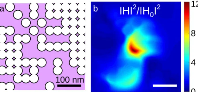
2.4. Influence of Low Structural Details on the Behavior of the Optimized Dielectric Antenna
Since GA designs are more elaborate than commonly studied optical nanoantennas, their experimental nanofabrication can be challenging. To provide insights towards this issue, we created a new nanostructure, shown in figure 4a, used as an extreme case in which the sharp edges of the design, which are challenging to fabricate, are modified. This rough design follows the general shape of the optimized structure in figure 3a, but instead of using parallelepipeds made of dielectric or air, we perforated a block of silicon with dimensions of 366x366 nm2 in (x,y) and 92 nm in z, by cylinders made of
air with diameters of 38 nm and a height of 92 nm. The magnetic intensity distribution produced by this rough design that would be significantly easier to fabricate by focused ion beam milling or e-beam lithography, is shown in figure 4b. Comparing the rough structure with the original structure, we can observe that the spatial distribution of the magnetic intensity is almost not affected by changing the sharp edges, and the intensity enhancement is slightly lowered, but is still significantly larger (more than 4 times) than the enhancement recorded above a hollow nanodisk (figure 3b and d). This result indicates that once the general GA design is defined, the fine details should only contribute marginally to the field enhancement, increasing the compatibility of the GA designs with experimental nanofabrication.
Figure 4. Low detailed design structure. a) Schematic of an optical nanoantenna where the parallelepipeds of air are replaced by cylinders of 38 nm diameter in the optimized GA design, in order to render the effect of a low detailed structure. b) Magnetic intensity enhancement of a in a plane 2 nm away in z from the antenna.
3. Conclusion
In conclusion, we demonstrated that evolutionary algorithm approaches are a powerful tool for designing dielectric optical nanostructures, and are able to enhance the magnetic intensity of light 5 times more than what state-of-the-art photonic nanoantennas allow nowadays. Furthermore, together with the fine-tuning of the optimized design, we demonstrated that although GA designs are more elaborate than most of the optical nanoantennas known so far, the optimized shape is weakly dependent on fine structural details (such as sharp edges), and that a rough nanofabrication process would still lead to a much larger enhancement of magnetic field intensities than hollow nanodisks. We believe that this approach will lead to a leap forward in the design of optical nanodevices to study and increase the coupling between magnetic light and matter. In addition, we envision a broad application of the GA approach by setting different selection criteria, such as maximizing the ratio between magnetic over electric intensities, or setting multiple selection criteria at once,
0 4 8 12 a b 100 nm IHI2/IH0I2
and by using alternative materials or wavelengths. In particular, the use of plasmonic materials should be of interest to enhance the magnetic field at near-infrared telecommunications wavelengths, where erbium ions exhibit strong magnetic dipolar emission.[54]
Supporting Information
Supporting Information is available from the Wiley Online Library or from the author.
Conflict of Interest
The authors declare no conflict of interest.
Acknowledgement
M.M acknowledges support from the French “Investissements d’Avenir” program (Labex MATISSE), the DIM Nano-K program from “Région Ile de France”, the CNRS emergence program and the ANR tremplin under reference ANR-17-ERC3-0006-01. S. B.
acknowledges support from LABEX WIFI (Laboratory of Excellence within the French Program “Investments for the Future”) under references LABX-24 and ANR-10-IDEX-0001-02 PSL*.
References
[1] L. D. Landau, E. M. Lífshíts, and L. Pitaevskii, Electrodynamics of continuous media (Pergamon press Oxford, 1984), Vol. 8.
[2] R. D. Cowan, The theory of atomic structure and spectra (Univ of California Press, 1981), Vol. 3.
[3] M. Burresi, D. Van Oosten, T. Kampfrath, H. Schoenmaker, R. Heideman, A. Leinse, and L. Kuipers, Science. 2009, 326, 550.
[4] H. Giessen and R. Vogelgesang, Science. 2009, 326, 529.
[5] D. G. Baranov, R. S. Savelev, S. V. Li, A. E. Krasnok, and A. Alù, Laser. Photonics. Rev.a 2017, 11, 1600268.
[6] V. K. Valev, A. O. Govorov, and J. Pendry, Adv. Opt. Mater. 2017, 5. [7] Z. Xi and H. Urbach, Phys. Rev. Lett. 2017, 119, 053902.
[8] A. Manjavacas, R. Fenollosa, I. Rodriguez, M. C. Jiménez, M. A. Miranda, and F. Meseguer, J. Mater. Chem. C. 2017, 5, 11824.
[9] N. Noginova, Y. Barnakov, H. Li, and M. Noginov, Opt. Express. 2009, 17, 10767. [10] S. Karaveli and R. Zia, Opt. Lett. 2010, 35, 3318.
[11] S. Karaveli and R. Zia, Phys. Rev. Lett. 2011, 106, 193004.
[12] T. H. Taminiau, S. Karaveli, N. F. van Hulst, and R. Zia, Nat. Commun. 2012, 3, 979. [13] S. Karaveli, S. Wang, G. Xiao, and R. Zia, ACS. Nano. 2013, 7, 7165.
[14] L. Aigouy, A. Cazé, P. Gredin, M. Mortier, and R. Carminati, Phys. Rev. Lett. 2014, 113, 076101.
[15] F. T. Rabouw, P. T. Prins, and D. J. Norris, Nano. Lett. 2016, 16, 7254.
[16] A. B. Evlyukhin, C. Reinhardt, A. Seidel, B. S. Luk’yanchuk, and B. N. Chichkov, Phys.
Rev. B. 2010, 82, 045404.
[17] A. García-Etxarri, R. Gómez-Medina, L. S. Froufe-Pérez, C. López, L. Chantada, F. Scheffold, J. Aizpurua, M. Nieto-Vesperinas, and J. Sáenz, Opt. Express. 2011, 19, 4815. [18] A. B. Evlyukhin, S. M. Novikov, U. Zywietz, R. L. Eriksen, C. Reinhardt, S. I. Bozhevolnyi, and B. N. Chichkov, Nano. Lett. 2012, 12, 3749.
[19] B. Rolly, B. Bebey, S. Bidault, B. Stout, and N. Bonod, Phys. Rev. B. 2012, 85, 245432. [20] M. K. Schmidt, R. Esteban, J. Sáenz, I. Suárez-Lacalle, S. Mackowski, and J. Aizpurua,
Opt. Express. 2012, 20, 13636.
[21] P. Albella, M. A. enz, and J. Aizpurua, J. Phys. Chem. C. 2013, 117, 13573.
[22] T. Coenen, J. Van De Groep, and A. Polman, ACS. Nano. 2013, 7, 1689. [23] X. Zambrana-Puyalto and N. Bonod, Phys. Rev. B. 2015, 91, 195422. [24] T. Feng, Y. Xu, Z. Liang, and W. Zhang, Opt. Lett. 2016, 41, 5011.
[25] A. I. Kuznetsov, A. E. Miroshnichenko, M. L. Brongersma, Y. S. Kivshar, and B. Luk’ uk Science. 2016, 354, aag2472.
[26] M. A. van de Haar, J. van de Groep, B. J. Brenny, and A. Polman, Opt. Express. 2016, 24, 2047.
[27] T. Feng, W. Zhang, Z. Liang, Y. Xu, and A. E. Miroshnichenko, ACS. Photonics. 2017, 5, 678.
[28] J. Li, N. Verellen, and P. Van Dorpe, ACS. Photonics. 2017, 4, 1893.
[29] E. Calandrini, A. Cerea, F. De Angelis, R. P. Zaccaria, and A. Toma, Nanophotonics. 2018,
8, 45.
[30] J. Zeng, M. Darvishzadeh-Varcheie, M. Albooyeh, M. Rajaei, M. Kamandi, M. Veysi, E. O. Potma, F. Capolino, and H. K. Wickramasinghe, ACS. Nano. 2018, 12, 12159.
[33] D. N. Chigrin, D. Kumar, D. Cuma, and G. von Plessen, ACS. Photonics. 2015, 3, 27. [34] M. Mivelle, T. Grosjean, G. W. Burr, U. C. Fischer, and M. F. Garcia-Parajo, ACS.
Photonics. 2015, 2, 1071.
[35] C. Zhang, J. Fang, W. Yang, Q. Song, and S. Xiao, Adv. Opt. Mater. 2017, 5, 1700469. [36] S. Sun, C. Zhang, H. Zhang, Y. Gao, N. Yi, Q. Song, and S. Xiao, Chin. Opt. Lett. 2018, 16, 050008.
[37] T. Feng, Y. Zhou, D. Liu, and J. Li, Opt. Lett. 2011, 36, 2369.
[38] R. Hussain, S. S. Kruk, C. E. Bonner, M. A. Noginov, I. Staude, Y. S. Kivshar, N. Noginova, and D. N. Neshev, Opt. Lett. 2015, 40, 1659.
[39] C. Ernandes, H.-J. Lin, M. Mortier, P. Gredin, M. Mivelle, and L. Aigouy, Nano. Lett. 2018,
18, 5098.
[40] M. Sanz-Paz, C. Ernandes, J. U. Esparza, G. W. Burr, N. F. van Hulst, A. Maitre, L. Aigouy, T. Gacoin, N. Bonod, M. F. Garcia-Parajo, S. Bidault, and M. Mivelle, Nano. Lett. 2018,
18, 3481.
[41] P. R. Wiecha, C. Majorel, C. Girard, A. Arbouet, B. Masenelli, O. Boisron, A. Lecestre, G. Larrieu, V. Paillard, and A. Cuche, Appl. Opt. 2019, 58, 1682.
[42] A. Vaskin, S. Mashhadi, M. Steinert, K. E. Chong, D. Keene, S. Nanz, A. Abass, E. Rusak, D.-Y. Choi, I. Fernandez-Corbaton, T. Pertsch, C. Rockstuhl, M. A. Noginov, Y. S. Kivshar, D. N. Neshev, N. Noginova, and I. Staude, Nano. Lett. 2019, 19, 1015.
[43] B. Choi, M. Iwanaga, Y. Sugimoto, K. Sakoda, and H. T. Miyazaki, Nano. Lett. 2016, 16, 5191.
[44] A. I. Kuznetsov, A. E. Miroshnichenko, Y. H. Fu, J. Zhang, and B. Luk’Y uk Sci. Rep. 2012, 2, 492.
[45] S. Molesky, Z. Lin, A. Y. Piggott, W. Jin, J. Vucković, and A. W. Rodriguez, Nat.
Photonics. 2018, 12, 659.
[46] T. Feichtner, O. Selig, M. Kiunke, and B. Hecht, Phys. Rev. Lett. 2012, 109, 127701. [47] T. Feichtner, O. Selig, and B. Hecht, Opt. Express. 2017, 25, 10828.
[48] P. R. Wiecha, A. Arbouet, C. Girard, A. Lecestre, G. Larrieu, and V. Paillard, Nat.
Nanotechnol. 2017, 12, 163.
[49] A. Y. Piggott, J. Lu, K. G. Lagoudakis, J. Petykiewicz, T. M. Babinec, and J. Vučk v ć
Nat. Photonics. 2015, 9, 374.
[50] L. Su, A. Y. Piggott, N. V. Sapra, J. Petykiewicz, and J. Vuckovic, ACS. Photonics. 2017, 5, 301.
[51] Z. Yu, H. Cui, and X. Sun, Photonics. Res. 2017, 5, B15. [52] T. Asano and S. Noda, Opt. Express. 2018, 26, 32704.
[53] Z. Jin, S. Mei, S. Chen, Y. Li, C. Zhang, Y. He, X. Yu, C. Yu, J. K. Yang, and B. Luk’ uk ACS. Nano. 2019.
[54] D. Li, M. Jiang, S. Cueff, C. M. Dodson, S. Karaveli, and R. Zia, Phys. Rev. B. 2014, 89, 161409.