• Aucun résultat trouvé

Interplay Between Electron Over-Heating and ac Josephson Effect

N/A
N/A
Protected

Academic year: 2021

Partager "Interplay Between Electron Over-Heating and ac Josephson Effect"

Copied!
9
0
0

Texte intégral

(1)

HAL Id: hal-01257485

https://hal.archives-ouvertes.fr/hal-01257485v3

Submitted on 27 May 2016

HAL is a multi-disciplinary open access

archive for the deposit and dissemination of

sci-entific research documents, whether they are

pub-lished or not. The documents may come from

teaching and research institutions in France or

abroad, or from public or private research centers.

L’archive ouverte pluridisciplinaire HAL, est

destinée au dépôt et à la diffusion de documents

scientifiques de niveau recherche, publiés ou non,

émanant des établissements d’enseignement et de

recherche français ou étrangers, des laboratoires

publics ou privés.

Interplay Between Electron Over-Heating and ac

Josephson Effect

Alessandro de Cecco, Kévin Le Calvez, Benjamin Sacépé, Clemens

Winkelmann, Hervé Courtois

To cite this version:

Alessandro de Cecco, Kévin Le Calvez, Benjamin Sacépé, Clemens Winkelmann, Hervé Courtois.

Interplay Between Electron Over-Heating and ac Josephson Effect. Physical Review B, American

Physical Society, 2016, 93 (18), pp.180505. �10.1103/PhysRevB.93.180505�. �hal-01257485v3�

(2)

Interplay Between Electron Over-Heating and ac Josephson Effect

A. De Cecco1,2, K. Le Calvez1,2, B. Sac´ep´e1,2, C. B. Winkelmann1,2 and H. Courtois1,21, 2

1 1

Universit´e Grenoble Alpes, Institut N´eel, 25 Avenue des Martyrs, 38042 Grenoble, France

2 2

CNRS, Institut N´eel, 25 Avenue des Martyrs, 38042 Grenoble, France (Dated: May 27, 2016)

We study the response of high-critical current proximity Josephson junctions to a microwave excitation. Electron over-heating in such devices is known to create hysteretic dc voltage-current characteristics. Here we demonstrate that it also strongly influences the ac response. The interplay of electron over-heating and ac Josephson dynamics is revealed by the evolution of the Shapiro steps with the microwave drive amplitude. Extending the Resistively Shunted Josephson junction model by including a thermal balance for the electronic bath coupled to phonons, a strong electron over-heating is obtained.

A normal metal (N) coupled to two superconducting electrodes (S) constitutes a Josephson junction, that is, a device capable of sustaining a dissipationless supercur-rent [1–3]. The small normal state resistance and lead-to-lead capacitance of SNS junctions make these strongly overdamped in the RCSJ model [1], meaning that the quantum phase dynamics is intrinsically non-hysteretic. Still, hysteresis is observed in the voltage-current (V -I) characteristics of high-critical current SNS junctions due to electronic over-heating associated to the sudden onset of dissipation when the bias exceeds the critical current [4]. Besides, under a microwave excitation at frequency ν, the junction characteristics display voltage plateaus at Vn = nhν/2e with n an integer [5]. These so-called

Shapiro steps are due to the phase-locking of the super-current oscillations at the Josephson frequency 2eV /h to the microwave. Shapiro steps have been frequently used for studying the phase dynamics of a variety of Joseph-son junctions [6–10]. This includes in particular junctions based on novel materials [11–21] where the absence of odd steps can be the signature of topological transport. Still, the interplay between the electron over-heating and the ac Josephson dynamics has been so far overlooked.

In this paper, we discuss the response of high-critical current proximity Josephson junctions to a microwave excitation. We demonstrate the prominent role of elec-tronic over-heating in the Shapiro steps map. Low-index steps can be masked by the switching to the resistive state. A simple model explains this behavior as well as the observation of a sharp discontinuity in the measured critical current when the ac current is increased.

We have fabricated Nb-Au-Nb junctions using a lift-off lithography technique based on an Al-Mo metallic bilayer as a shadow mask [22], which avoids the deterioration of Nb superconducting properties by organic contamina-tion. Conventional e-beam lithography, followed by a dry etch of the Mo top layer and a wet etch of the Al bottom layer, produces a locally suspended Mo mask. A shadow evaporation of Au (N island) and Nb (S leads) is per-formed through this mask at opposite angles. The edge roughness of the structures (see Fig. 1c inset) arises from the granularity of the Mo mask. The junctions were all

about 210 nm wide, the separation between the Nb elec-trodes ranging from 180 to 500 nm, while the Au part was about 200 nm longer in order to ensure a good over-lap with each electrode. The normal-state resistance of the junctions can be related to a diffusion constant D in Au of about 100 cm2/s. The critical temperature of

the Nb electrodes is 8.5 K. Table 1 lists the main device parameters for the different junctions investigated.

Transport measurements were performed at tempera-tures down to 100 mK. Fig.1a-b show V-I characteristics of a typical sample. At low temperature, a strong super-conducting branch is observed (Fig. 1a), with a large critical current Ic exceeding 100 µA. This is achieved

owing to the short length of the Au bridge and the high interface transparencies. Above Ic, the V-I

characteris-tic switches to the ohmic branch, characterized by the normal-state resistance RN. When the current is

low-ered again, the V -I characteristic remains on the ohmic branch down to the so-called retrapping current Ir< Ic.

This pronounced hysteretic behaviour is of thermal origin and is typical of SNS junctions with a large critical cur-rent density [4]. The retrapping current can be roughly thought of as the value of the critical current at a bias-dependent, higher electronic temperature T∗, determined

by the thermal balance between the dissipated Joule heat and the coupling to the phonon bath. Conversely, T∗ is

also the temperature scale above which Ir and Ic merge

(see Fig. 1c) and the behavior of the junction becomes non-hysteretic (Fig. 1b).

The temperature dependence of the critical current is displayed in Fig. 1c. The properties of long SNS junctions depend only little on the superconducting elec-trodes’ energy gap ∆, but are mainly governed by the normal island’s Thouless energy [2,8] ETh= ¯hD/L2≪

∆, where D is the diffusion constant and L the length of N. Within the Usadel equations framework and assuming kBT > ETh, the critical current Ic follows [23]:

eRNIc= η ETh 32 3 + 2√2  2πkBT ETh 3/2 exp − s 2πkBT ETh ! . (1) Here the phenomenological parameter η < 1 describes a

(3)

2 No L R N E fit Th Leff η I 0 c I 0 r T∗

(nm) (Ω) (µeV) (nm) (µA) (µA) (K) J1 225 2.4 28.1 474 0.86 104 33 1.9 J2 300 2.1 23.6 536 0.89 78 45 1.4 J3 180 1.7 49.6 390 0.78 178 35 2.6 J4 500 3.6 9.9 785 0.67 14 2 1.1 TABLE I. Parameters of the reported samples. In all samples, the Au strip width W is 210±10 nm, its thickness is 20 nm for sample J1 and 30 nm for samples J2 - J4, while Nb thickness is 60 nm for sample J1 and 90 nm for samples J2-J4. L is the Nb-Nb distance. RN is the normal-state resistance measured

at 4.2 K. Efit

Th and η are the fitting parameters in Eq. 1.

Leff =p¯hD/EThfit is the effective junction length. Ic0 and I 0 r

the values of the critical/retrapping currents respectively at T → 0 and in the absence of magnetic field and microwave excitations. T∗is defined by I

c(T∗) = Ir0.

reduction in the critical current related, for instance, to non-ideal interfaces. A very good fit to the data is ob-tained in all devices, with η always exceeding 0.6, see Ta-ble 1. The effective length Leff =p¯hD/ETh associated

to the fit Thouless energy Efit

Th exceeds the mere

separa-tion L between the electrodes. It should indeed include about twice the superconducting coherence length since Andreev reflections take place in S over such a length [23]. The dependence of the critical current on a perpendicu-lar magnetic field (Fig. 1d) shows both a quasi-gaussian monotonic decay associated to dephasing and a oscilla-tory part arising from interference effects [24,25].

We now turn to the effect of a microwave excitation on the V-I characteristics. Microwave signals in the fre-quency range 1 to 26 GHz and with a power Pµ were

ap-plied to the shielded cavity containing the sample. As the impedance of our samples is small compared to the esti-mated line impedance at high frequency, the samples are still current-biased in the microwave regime. The color map of Fig. 2a shows the differential resistance dV /dI (obtained by numerical derivation) as a function of the dc bias current I and the microwave current Iµ ∝ Pµ1/2

at a frequency ν = 6 GHz. The supercurrent branch and the Shapiro steps (up to an index exceeding 10) appear as dark regions, with zero differential resistance. At large excitation amplitudes, Fig. 2a map is symmetric in I and the Shapiro steps’ widths oscillate with the microwave ex-citation amplitude, producing a well-known pattern [1]. At small microwave current Iµ, the hysteresis appears

through the asymmetry of the map with respect to I. Strikingly, several low-index steps do not appear in the (positive) current branch corresponding to a current in-creasing from zero to above the critical current Ic.

Indi-vidual V-I characteristics clearly demonstrate (Fig. 2 b-d) that the absence of these steps stems from the volt-age directly jumping from zero up to about RNIc, which

corresponds to the ohmic branch. Steps corresponding

FIG. 1. V-I characteristics of device J3 measured at tem-peratures of (a) 100 mK and (b) 4.2 K. The arrows indicate the sweeping direction of the current bias. (c) Temperature dependence of the critical current Ic(black dots) and the

re-trapping current Ir(red dots) for sample J3. The green dotted

line represents a fit to Eq. (1). Inset: AFM image of a typi-cal Nb-Au-Nb junction. (d) Magnetic-field dependence of the critical current Ic (black dots) and the retrapping current Ir

(red dots) (T = 280 mK, device J1). Steps in current values appearing at large magnetic field are artifacts.

to voltages below RNIc thus cannot be detected. This

behavior here is clearly distinct from the discussion of re-cent experiments on Josephson junctions based on topo-logical insulators, in which odd-index Shapiro steps are predicted to be absent.

Let us now consider the behavior of the critical cur-rent as a function of the microwave curcur-rent amplitude Iµ. In a current bias picture, the microwave irradiation

adds adiabatically an oscillatory excursion Iµto the bias

current I, so that the current oscillates between I − Iµ

and I + Iµ [9]. In a quasi-static regime, switching to

the resistive state then occurs at a lower critical current Ic− Iµ. Once the junction has switched, it remains in

the resistive state due to hysteresis. One expects there-fore a linear suppression of Ic with increasing Iµ, as seen

in Fig. 2a. We attribute the slight downward deviation from linear behavior to a small increase in the electronic temperature at high microwave power. On the retrap-ping branch, a similar decay of the retrapretrap-ping current Ir

with the microwave current Iµ is observed.

In order to provide a quantitative description, we need to consider the energy relaxation from the normal metal electronic population. In the present temperature range, electron-phonon scattering is the dominant mechanism. The related coupling power between electrons at a tem-perature Teand phonons at a temperature Tphis Pe−ph =

ΣU (T5

(4)

cou-FIG. 2. (a) Differential resistance map as a function of the dc current bias I and the microwave excitation amplitude Iµ

for a frequency ν = 6 GHz (device J2, Tbath = 100 mK).

The white arrow indicates the sweeping direction of the dc current bias. The top black arrows point to the individual V-I curves taken at microwave drives of (b) 0.020 (c) 0.035 (d) 0.056 (a.u.). Voltage is normalized to hν/2e. (e) Calculated differential resistance map, including thermal effects.

pling constant and U is the metal volume. Considering a retrapping temperature T∗ of 1 to 3 K, the related rate

τ−1

e−ph≈ 0.16×T

3GHz in Au [26] is in the low GHz range

(≈ 0.4 GHz in J2 at T∗= 1.4 K for instance). In most of

the frequency range investigated here, the thermal relax-ation is thus slow compared to the microwave (τ−1

e−ph< ν)

so that the electronic temperature can be considered as almost constant with time at a given (I,Iµ) bias point.

We consider a Resistively Shunted Junction (RSJ) model [1] with a current bias. The time-dependent cur-rent i(t) = I + Iµsin(2πνt) through the junction is

con-sidered as the sum of the ohmic current v/R and the Josephson current Icsin ϕ, where ϕ is the phase

differ-ence across the junction:

i(t) = I + Iµsin(2πνt) = Icsin ϕ + v/R. (2)

The dependent voltage v relates to the time-derivative of the phase as v(t) = ¯h ˙ϕ/2e from the

sec-ond Josephson relation. From Eq. (2), the phase dy-namics can be modeled as that of a massless particle of position ϕ in a tilted washboard potential U (ϕ) = −¯h[Iccos ϕ+i(t)]/2e. The potential slope is proportional

to the current bias i(t): its average is thus determined by I and it oscillates with an amplitude given by Iµ. For

large enough I or Iµ, the particle rolls down the slope.

The Shapiro steps at voltage values Vn= n hν/2e

corre-spond to the particle hopping down by n minima during one microwave period.

We can write the instantaneous Joule power:

p(t) = i(t) · v(t) = Ic ¯ h 2eϕ sin ϕ +˙ 1 R  ¯h 2eϕ˙ 2 . (3)

The first term relates to the change in the Josephson energy. It is zero in average and does not contribute to the average power P dissipated over one cycle. Only the second term, which is the Joule power across the junction resistance, dissipates. It can be non-zero in average even though the average voltage V is zero.

At this point, we now introduce a heat balance where the dissipated power P is balanced by the electron-phonon coupling power Pe−ph. The related temperature elevation acts on the phase dynamics through the tem-perature dependence of the critical current following Eq. (1). Using Eqs. (2) and (3) and taking the volume U as a free parameter, we have numerically calculated the time-dependence of the phase, the dissipated power and the ensuing electronic temperature Te for every (I,Iµ) bias

point, which gives access to the related dc voltage drop V . Fig. 2e shows the calculated differential resistance for device J2’s parameters. For the best fit, the volume U was chosen as 10 times the physical volume. This can be explained by both the inverse proximity effect in the leads in the vicinity of the N-S interface and the thermal conductance of the leads between the N island and the N metal regions of the leads. A semi-quantitative agree-ment for the differential resistance between Fig. 2a and

2e is readily seen.

The associated temperature map of Fig. 3a highlights the importance of dissipation in the ac phase dynamics in SNS junctions. Strikingly, the electronic temperature varies significantly as a function of the microwave current bias: the temperature increases from the bath tempera-ture of 0.1 K up to above 2 K. On the first Shapiro step, the temperature is already of about 1 K. Even for zero dc current I and hence zero average voltage V , electrons in N are significantly overheated at large microwave drives, see Fig. 3a inset. The Shapiro steps structure appears also on the temperature map, as can be seen in Fig. 3a and more clearly in Fig. 3b as wiggles in every curve, especially the curve (2).

Both the data (Fig. 2a) and the calculations (Fig. 2e) exhibit a sudden drop of the critical current Ic as the

(5)

4

FIG. 3. (a) Calculated electronic temperature Te map

cor-responding to the situation of Fig. 2, i.e. for device J2 at Tbath = 100 mK. Inset: Line cut of this map showing the

electronic temperature at zero dc bias current as a function of the microwave current and calculated value of the critical current at this electronic temperature. The dashed line indi-cates the Ic(Te) = Iµ correspondence. (b) Line cuts of the

map (a) showing the dependence of the electronic tempera-ture as a function of the dc bias current I at different values of the microwave current Iµindicated by arrows at the top of

the map.

current Iµ= I∗ (of about 0.04 in Fig. 2a). As shown in

Fig. 3a inset, the microwave amplitude Iµat this point is

approximately equal to the critical current Ic(Te) at the

electronic temperature at zero bias, so that no supercur-rent can be established due to the electronic overheating at this point of the V-I characteristics. The numerical solution of the phase dynamics illustrates this precisely: while at an ac drive below I∗ the particle oscillates in a

single washboard valley, above I∗it hops back and forth

between two valleys [27]. Let us note that this feature would not appear if the microwave amplitude would be swept at a fixed (and low) dc bias current.

We have obtained a good agreement between exper-iment and calculation at every investigated microwave frequency up to 26 GHz. At higher frequency, as dissi-pation increases with excitation frequency ν as ν2, the

electron over-heating is much increased in the supercon-ducting state (V = 0). The two currents Ic(Iµ) and

Ir(Iµ) are thus seen to merge before Ir approaches zero

[27] and no discontinuity is observed.

The interplay of electron over-heating and ac Joseph-son dynamics discussed here is prominent in junctions that are hysteretic in dc. Indeed, when driving our same devices to non-hysteretic conditions, either by applying a magnetic field (Fig. 4a) or increasing the temperature (Fig. 4b), the usual Shapiro pattern is recovered [1]. This is evidenced by the good agreement of the width of the n = 0 step with the standard Bessel function expression (white dotted lines in Fig. 4a and b). The crossover between the overheating regime and the isothermal

be-FIG. 4. Differential resistance maps as a function of I and Iµ for ν = 6 GHz in non-hysteretic conditions, (a) at base

temperature and under a magnetic field of 100 mT (device J2), and (b) at a bath temperature of about 4.2 K (device J3, no magnetic field). The white lines represent the usual Bessel-function-like amplitude of the step n = 0.

haviors depends not only on the junction critical current amplitude but also on the coupling to the thermal bath. In summary, we have evidenced that electron over-heating is of paramount influence in the microwave re-sponse of Josephson junctions. Exploring the microwave response of Josephson junctions involves variable elec-tronic temperatures, which is of uttermost importance for the complete analysis of devices based on new mate-rials like topological conductors.

We acknowledge financial support from the ANR con-tract ”Nanoquartets” and the LANEF project ”UHV-NEQ”. Samples were fabricated at the Nanofab platform at CNRS, Grenoble. We thank A. Nabet and D. van Zan-ten for help in the experiments, S. Samaddar and J. P. Pekola for discussions.

[1] K. K. Likharev, Dynamics of Josephson Junctions and Circuits(Gordon and Breach, 1991).

[2] H. Courtois, P. Gandit, B. Pannetier, and D. Mailly, Su-perlatt. and Microstruct. 25, 721 (1999).

[3] L. Angers, F. Chiodi, G. Montambaux, M. Ferrier, S. Gu´eron, H. Bouchiat, and J. C. Cuevas, Phys. Rev. B 77, 165408 (2008).

[4] H. Courtois, M. Meschke, J. T. Peltonen, and J. P. Pekola, Phys. Rev. Lett. 101, 067002 (2008).

[5] S. Shapiro, Phys. Rev. Lett. 11, 80 (1963).

[6] K. W. Lehnert, N. Argaman, H. R. Blank, K. C. Wong, S. J. Allen, E. L. Hu, and H. Kroemer, Phys. Rev. Lett. 82, 1265 (1999).

[7] P. Dubos, H. Courtois, O. Buisson, and B. Pannetier, Phys. Rev. Lett. 87, 206801 (2001).

[8] H. le Sueur, P. Joyez, H. Pothier, C. Urbina, and D. Est`eve, Phys. Rev. Lett. 100, 197002 (2008).

[9] F. Chiodi, M. Aprili, and B. Reulet, Phys. Rev. Lett. 103, 177002 (2009).

[10] B. Dassonneville, M. Ferrier, S. Gu´eron, and H. Bouchiat, Phys. Rev. Lett. 110, 217001 (2013).

(6)

Bakkers, L. P. Kouwenhoven, and S. De Franceschi, Sci-ence 309, 272 (2005).

[12] L. Fu, C. L. Kane, and E. J. Mele, Phys. Rev. Lett. 98,106803 (2007).

[13] J.-P. Cleuziou, W. Wernsdorfer, S. Andergassen, S. Flo-rens, V. Bouchiat, Th. Ondar¸cuhu, and M. Monthioux, Phys. Rev. Lett. 99, 117001 (2007).

[14] M. Fuechsle, J. Bentner, D. A. Ryndyk, M. Reinwald, W. Wegscheider, and C. Strunk, Phys. Rev. Lett. 102, 127001 (2009).

[15] L. Jiang, D. Pekker, J. Alicea, G. Refael, Y. Oreg and F. von Oppen, Phys. Rev. Lett. 107, 236401 (2011). [16] F. Dominguez, F. Hassler, and G. Platero, Phys. Rev. B

86140503 (2012).

[17] D. M. Badiane, L. I. Glazman, M. Houzet, and J. S. Meyer, Comptes Rendus Physique 14, 840 (2013). [18] L. P. Rokhinson, X. Liu, and J. K. Furdyna, Nature Phys.

8, 795 (2012).

[19] L. Galletti, S. Charpentier, M. Iavarone, P. Lucignano, D. Massarotti, R. Arpaia, Y. Suzuki, K. Kadowaki, T. Bauch, A. Tagliacozzo, F. Tafuri, and F. Lombardi, Phys. Rev. B 89, 134512 (2014).

[20] V. S. Pribiag, A. J. A. Beukman, F. Qu, M. C. Cassidy, C. Charpentier, W. Wegscheider and L. P. Kouwenhoven, Nat. Nanotech. 10, 593 (2015).

[21] J. Wiedenmann, E. Bocquillon, R. S. Deacon, S. Hartinger, T. M. Klapwijk, L. Maier, C. Ames, C. Br¨une, K. Ishibashi, S. Tarucha, H. Buhmann, L. W. Molenkamp, Nature Comm. 7, 10303 (2016).

[22] S. Samaddar, D. van Zanten, A. Fay, B. Sac´ep´e, H. Cour-tois, and C. B. Winkelmann, Nanotechnology 24, 375304 (2013).

[23] P. Dubos, H. Courtois, B. Pannetier, F. K. Wilhelm, A. D. Zaikin, and G. Sch¨on, Phys. Rev. B 63, 064502 (2001). [24] F. Chiodi, M. Ferrier, S. Gu´eron, J. C. Cuevas, G. Mon-tambaux, F. Fortuna, A. Kasumov, and H. Bouchiat, Phys. Rev. B 86, 064510 (2012).

[25] J. C. Cuevas and F. S. Bergeret, Phys. Rev. Lett. 99, 217002 (2007).

[26] P. M. Echternach, M. R. Thoman, C. M. Gould, and H. M. Bozler, Phys. Rev. B 46, 10339 (1992).

[27] See Supplemental Material for details on the phase dy-namics calculation and data at various microwave frequen-cies.

(7)

1

Supplemental Materials: Interplay Between Electron Over-Heating and ac Josephson

Effect

In this supplemental materials part, we provide some more details about the numerical calculation of the differential resistance map under microwave irradiation, as well as the calculation results supporting the explanation for the discontinuity observed in the differential resistance map. We also discuss additional experimental data obtained at different values of the microwave frequency.

NUMERICAL CALCULATIONS

Our model is an extension of the RSJ model with the temperature dependence of the critical current (Eq. (1) of the main text), the electronic temperature Te in N being governed by the thermal balance between the Joule power

and the coupling to phonons. We here neglect other heat transport channels out of N, which will eventually lead to a somewhat lower temperature.

A sharp discontinuity in the differential conductance map at 6 GHz is described in the main text, see Fig. 2 of the main paper. Fig. S1shows both a zoom of the map and the time-dependence of the phase at two points at the same dc current bias, but at an ac current signal amplitude just below and above the threshold. While the mean voltage is zero in every case, the phase’s excursion is larger in amplitude at larger ac signal. It exceeds 2π in the latter case, meaning that the effective particle travels over two neighboring minima of the potential landscape. The related dissipation makes the electronic temperature rise and the effective critical current drop, resulting in a sharp change in the differential conductance map.

The agreement with experimental data at the same frequency is remarkable at every microwave frequency inves-tigated. Fig. 2 in the main paper displays data and calculation at 6 GHz, while Fig. S2 and Fig. S3 in this supplementary materials display similar information at 8.8 GHz and 24.2 GHz.

Here we also provide the map of the temperature derivative with respect to the current bias, see Fig. S4. This plot highlights the appearance in the temperature map of the Shapiro steps structure.

BEHAVIOR AT HIGHER FREQUENCY

In the higher frequency regime, we observe the appearance of fractional Shapiro steps at voltages Vn,m =

(n/m) hν/2e, where n and m are integers. This appears as thin zero-differential resistance regions at intermedi-ate positions compared to the integer steps in Fig. S3a, and short steps in Fig. S3b-d. Fractional Shapiro steps were already observed in similar devices [S1–S3]. Multiple Andreev Reflections as well as non-thermal out-of-equilibrium energy distribution function can contribute to this phenomena. As they are not included in our model, fractional steps are absent from the calculation results.

FIG. S1. (a) Zoom of the differential resistance map as a function of I and Iµat ν = 6 GHz (device J2, Tbath= 100 mK) shown

in Fig. 2e in the main paper. (b) Schematics showing the extent of the phase excursion at the two bias points. (c) Calculated time dependence of the phase at the bias points indicated by the crosses in (a). The dc current is zero in both cases.

(8)

FIG. S2. (a) Differential resistance map as a function of the dc current bias I and the microwave excitation amplitude Iµ for

a frequency ν = 8.8 GHz (device J2, Tbath = 100 mK). The white arrow indicates the sweeping direction of the dc current

bias. The top black arrows point to the individual V-I curves taken at microwave drives of (b) 0.010 (c) 0.043 (d) 0.072 (a.u.). Voltage is normalized to hν/2e. (e) Calculated differential resistance map, including thermal effects, see text for details. The related calculated temperature is displayed in (f), its derivative with respect to bias current is in (g).

At higher frequency, the dissipation at a given amplitude Iµ is larger. The dominating effect of the microwave

irradiation on the electronic population appears in Fig. S3 through the merging of the critical current and the retrapping current above an intermediate level of ac current bias Iµ > 0.02. As a consequence, no discontinuity is

observed in the differential resistance map. Still, the n = 1 step is missing at low microwave excitation.

[S1] P. Dubos, H. Courtois, O. Buisson, and B. Pannetier, Phys. Rev. Lett. 87, 206801 (2001).

[S2] K. W. Lehnert, N. Argaman, H. R. Blank, K. C. Wong, S. J. Allen, E. L. Hu, and H. Kroemer, Phys. Rev. Lett. 82, 1265 (1999).

[S3] M. Fuechsle, J. Bentner, D. A. Ryndyk, M. Reinwald, W. Wegscheider, and C. Strunk, Phys. Rev. Lett. 102, 127001 (2009).

(9)

3

FIG. S3. (a) Differential resistance map as a function of I and Iµ at ν = 24.2 GHz (device J2, T = 100 mK). The white

arrow indicates the sweeping direction of the dc current bias. The top black arrows point to the individual V-I curves taken at microwave drives of (b) 0.010 (c) 0.028 (d) 0.049 (a.u.). Voltage is normalized to hν/2e. (e) Calculated differential resistance map, including thermal effects, see text for details. The related calculated temperature is displayed in (f), its derivative with respect to bias current is in (g).

FIG. S4. Calculated map of the temperature derivative with respect to the current bias, including thermal effects, see text for details, corresponding to the case of Fig. 2 of the main paper, i.e. for sample J2 at a bath temperature of 100 mK.

Figure

TABLE I. Parameters of the reported samples. In all samples, the Au strip width W is 210 ± 10 nm, its thickness is 20 nm for sample J1 and 30 nm for samples J2 - J4, while Nb thickness is 60 nm for sample J1 and 90 nm for samples J2-J4
FIG. 2. (a) Differential resistance map as a function of the dc current bias I and the microwave excitation amplitude I µ
FIG. 4. Differential resistance maps as a function of I and I µ for ν = 6 GHz in non-hysteretic conditions, (a) at base temperature and under a magnetic field of 100 mT (device J2), and (b) at a bath temperature of about 4.2 K (device J3, no magnetic field
FIG. S1. (a) Zoom of the differential resistance map as a function of I and I µ at ν = 6 GHz (device J2, T bath = 100 mK) shown in Fig
+2

Références

Documents relatifs

Quantifying the effects of heating temperature, and combined effects of heating medium pH and recovery medium pH on the heat resistance of Salmonella typhimurium...

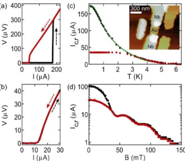
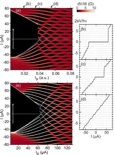
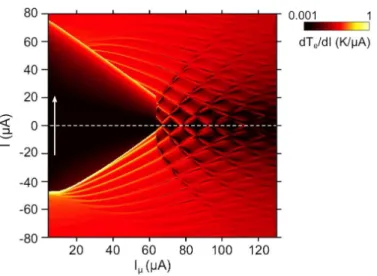
phase difference across the barrier becomes linear in time in the same way as the phase difference of the order parameter of a superconductor or of a superfluid in the presence of

model for determining the pressure on players with varying roles and skill levels in a team, as well as look more deeply in to the interaction of the number of players, excitement

Abstract This paper investigates the analytical properties of the sensitivity to the initial conditions on the calibration and simulation results of two karst spring

The hypersingular BIE residual function is found to be equal to the derivative of the strongly singular BIE residual when the same values of the boundary variables are substituted

Effects of the temperature and the incident electron current density on the total electron emission yield (TEEY) of polycrystalline diamond deposited by chemical vapor

Qi X, Ignatova S, Luo G et al (2010) Preparative isolation and purification of ginsenosides Rf, Re, Rd and Rb1 from the roots of Panax ginseng with a salt/containing solvent sys-

1: schematic overview of the measurement unit This equipment presented in detail in [1] is consisting of 4 main functions (Fig. A bar of the specimen is placed inside two