HAL Id: hal-02131990
https://hal.laas.fr/hal-02131990
Submitted on 16 May 2019
HAL is a multi-disciplinary open access
archive for the deposit and dissemination of
sci-entific research documents, whether they are
pub-lished or not. The documents may come from
teaching and research institutions in France or
abroad, or from public or private research centers.
L’archive ouverte pluridisciplinaire HAL, est
destinée au dépôt et à la diffusion de documents
scientifiques de niveau recherche, publiés ou non,
émanant des établissements d’enseignement et de
recherche français ou étrangers, des laboratoires
publics ou privés.
Drift effects and trap analysis of power-GaN-HEMT
under switching power cycling
Manuel González-Sentís, Patrick Tounsi, Alain Bensoussan, Arnaud Dufour
To cite this version:
Manuel González-Sentís, Patrick Tounsi, Alain Bensoussan, Arnaud Dufour. Drift effects and trap
analysis of power-GaN-HEMT under switching power cycling. Science of Electronics, Technologies of
Information and Telecommunication, SETIT’18, Dec 2018, Hammamet, Tunisia. �hal-02131990�
Drift effects and trap analysis of power-GaN-HEMT
under switching power cycling
Manuel A González-Sentís1,2,3, Patrick Tounsi2, Alain Bensoussan3, Arnaud Dufour1 1 CNES, Toulouse 31400, France
2 LAAS-CNRS, Toulouse 31400, France 3 IRT Saint-Exupéry, Toulouse 31423, France
Abstract. This paper studies the impact of the aging on power GaN tran-sistors in switching conditions. The devices under test are commercial discrete enhancement mode gallium-nitride HEMT. We present a power cycling test platform that controls the switching conditions such as fre-quency, duty cycle, and gate voltage; as well as drain current and drain voltage. We have measured specific parameters before and after the power cycling in order to detect indicators for each drift effect. We meas-ure not only the electrical parameters given by datasheet, but also the traps causing Dynamic On-State Resistance, an specific drift effect of this technology which compromises high frequency efficiency in switch-ing power converters.
Keywords: Power electronics, GaN HEMT, reliability, energy management,
wide bandgap semiconductors.
1
Introduction
In the last few years, gallium nitride (GaN) has become an excellent material for the fabrication of power transistors. Normally-off High-Electron Mobility Transistors (HEMTs) in AlGaN/GaN heterojunction are the most promising devices for space and automotive applications. This transistor offer offers very interesting performances for power switching converters such as high power densities and fast switching –resulting in smaller, lighter power converters– and low on-resistance. In addition, like other wide-bandgap materials, GaN is inherently radiation-hard material and tolerates higher operational temperatures.
Nevertheless, large-scale deployment of GaN HEMT remains limited because of in-sufficient technological maturity, high cost manufacturing and reliability. The compre-hension of the GaN devices specific failure mechanisms is unavoidable to use those devices in harsh environment under specific mission conditions.
As shown in [1], established test procedures from silicon are not sufficient to cover the reliability requirements for GaN, especially regarding charge trapping and Dynamic On-Resistance. Other authors [2] suggest new degradation indicators to track the evo-lution of power GaN HEMTS. Anyway, all of these studies agree that further studies
and new methods are necessary to better understand and measure the degradation mech-anisms of power GaN HEMT.
In order to obtain reliability data of power GaN devices, we apply a power-cycling test on discrete commercial devices. We choose the stress conditions to activate specific drift effects. The power-cycling test is described on section 2, the measurements are explained on section 3, and the results are shown on section 4.
2
Power-cycling test
2.1 Description and purpose
The aging of GaN devices depend on the kind of stress applied. That is the reason why the aim of this power-cycling test is to control all the electrical parameters. In power switching converters, the stress changes on each phase of the switching cycle [3]: During off-state phase, the device is under high internal electric field. The losses on
this phase are proportional to drain leakage current and drain voltage. A dynamic increase of on-resistance can be observed due to charge trapping effects (see fig.3) under high electric field in off-state [4].
In the on-state phase, losses are generated by high drain current and on-resistance. If on-resistance is increased dynamically by trapping effects, on-state losses can be significant.
During the switching phase, losses depend on the hard or soft switching operation and the duration of the switching event. The switching losses can dominate the over-all losses on hard switching mode.
2.2 Power-cycling set-up
We test discrete 200V GaN power devices with RDSON = 50mΩ, IDMAX = 8.5A and
VGS(TH)MAX=2.5V[5]. The devices are tested without packaging or heat sink; they are
soldered on the DUT PCB (see Fig.1). We plug the DUT PCB to the power board with a connector. After the stress, the DUT PCB is connected to the measure instruments.
We apply power-cycling tests to obtain reliability data in a short period of time. Two main sources of stress are regulated: the gate control and the power parameters. The gate control consists of a microcontroller board with different PWM channels
independently programmable. In order to protect the gate of the PWM overshoots, we use a gate driver compatible with GaN HEMT (LM5114), with up and pull-down resistors as recommended by manufacturers [6]. We can control the frequency, the duty cycle and the gate voltage for each device under test.
The power stress parameters controlled are the drain voltage VDS and the drain
cur-rent IDS, which is fixed by the power resistors.
Table 1. Power-cycling stress parameters
To fix the stress conditions we use a step stress: incremental levels of drain current in order to find the stress parameters that cause failure modes. We summarize the stress parameters in table 1. In order the study the influence of the gate voltage, we realize two power-cycling tests side by side: one with VG = 4V and other with VG = 5V.
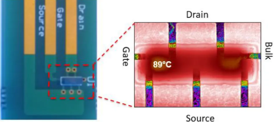
When fixing the stress parameter, we have taken into account the temperature. In [7] the authors show that high temperature swings (ΔT=100°C) can generate mechanical degradation, due to the high power densities in power GaN HEMTs. We want to study internal degradation mechanisms, not solder or packaging issues. In order to be sure that we do not activate thermo-mechanical failure mechanisms, such as delamination of solder due to high temperature swings, we measure the temperature with an infrared (IR) camera (see fig.2). We make sur that the chosen stress parameters do no heat the device under test at more than 100°C and ΔT<25°C. The switching frequency, an im-portant parameter that determines ΔT, is fixed to 1 kHz after the IR camera tests.
Fig. 2. DUT PCB and IR image of the device
Stress 1 Stress 2 Stress 3
Drain current 1 A 2A 4A
Drain voltage 10 V 20V 20V
Duty cycle 0.5 0.25 0.1
3
Measurements
The characterization consists of extracting the ID(VDS) curve, the ID(VGS) curve –from
which we deduce the threshold voltage VTH– and leakage current. Comparing the
dif-ferent stress and characterizations throughout the power cycling, we can identify spe-cific degradation phenomenon shown in table 2.
Table 2. Drift effects in GaN HEMTs, physical origin and measurement to test each effect,
based in [8].
The measuring instrument for I(V) curves and leakage currents is the HP4142B. To extract the C(V) curves we use the Agilent B1505. For the extraction of VTH we use the
linear extrapolation method in the linear region in the ID(VGS) curve, as shown in [9].
3.1 Trapping effects measurement Dynamic On-Resistance
One of the purposes of this work is to study the Dynamic RDSON evolution during the
power cycling. Dynamic On-Resistance, also called “current collapse” for RF GaN HEMT [10], generates additional losses in on-state and compromises high frequency efficiency. Dynamic RDSON is a transient phenomenon generated by trapped electrons
(see fig.3). The On-Resistance just after the turn-on is higher than the RDSON value given
by the datasheet. The trapped charge creates a local electric field that degrade the con-ductivity in the channel [10]. Trapped electrons must be released to achieve the nominal RDSON.
On the devices under test, this transient effect is on the order of microseconds de-pending on the stress applied. Dynamic RDSON transient is faster in high temperatures
because trapping and detrapping time-constants decrease with temperature [10]. The max RDSON depends on avaiable traps, i.e. impurities in the AlGaN layer or SiN
passivation, and dislocations and defects in the GaN buffer. A high VDS during off-state
and a long the time in off-state increase the RDSON after the turn-on. This is because
electrons have more energy (higher electric field) and more time to be trapped. When the time in off-state is long enough to fill all the traps, the RDSON will not increase
anymore.
DRIFT EFFECT PHYSICAL ORIGIN MEASUREMENT
Dynamic RDSON
increase
Trapping in GaN buffer and surface
trapping between drain and gate CG(VG) hysteresis measurement
Time-Depend-ent degradation
Generation of drain-source,
gate-channel paths and vertical breakdown Leakage current measurement VTH shift Electron trapping beneath the gate ID(VGS) characterisation
ID(VDS) for several VGS values
IG leakage
current
Path creation in the gate region, Trap-assisted tunnelling
CG(VG) hysteresis measurement
Fig. 3. Trapped electrons just after turn-on in a power GaN HEMT.
Traps measurement method
In order to investigate the evolution of traps during the aging of the transistors, we have realized CG(V) curves on the gate under sweeps from -4V to 6V and down from 6V to
-4V. The arrow nearby each curve marks sweep directions (see fig.2). We can observe a hysteresis in the capacitance expressed by a shift during the return sweep.
Fig. 4. CG(V) characteristic of the GaN HEMT before the power cycling test.
We realize the CG(V) measurement at 1MHz, at 300K and with a step of 50 mV. The
surface enclosed in the curve can be explained as injection and trapping off electrons [11]. Note that the surface enclosed is an electrical charge: capacitance (F) multiplied by a voltage (V).
4
Results and discussion
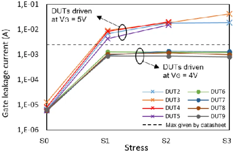
Figure 5 summarizes measured gate leakage current IG of eight DUTs during the
power cycling test. For the DUTs 2 to 5 (driven at VG = 5V), it is observed that IG rises
above the max given by the datasheet after the stress S1. However, they still work after S1. Nevertheless, DUT4 and DUT5 failed after S3, with IG > 100mA (the saturation of
the measuring instrument).
Fig. 5. Measured gate leakage current during the power cycling test. Note that DUTs 2 to 5
are driven at VG = 5V and DUTs 6 to 8 are driven at VG = 4V.
In contrast, the DUTs driven at VG = 4V present a gate leakage current below the max
given by datasheet. We observed that there is an initial degradation after S1, and then the gate leakage current remains stable during the rest of the power cycling.
Fig. 6. Measured gate threshold voltage during the power cycling. The curve shows that the
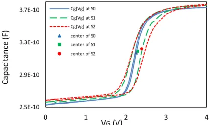
Figures 7 and 8 shows the evolution of the CG(V) curve of a DUT driven at VG=5V
and VG=4V during the power cycling.
Fig. 7. CG(V) characteristic a GaN HEMT driven at VG=5V. In blue, before the power
cy-cling, in green after stress S1 and in red after S2.
Fig. 7. CG(V) characteristic a GaN HEMT driven at VG=4V
We can observe that the hysteresis surface increases in devices driven at VG=5V
more than in devices driven at VG=4V. By observing the center of each surface, note
that the shift of the CG(V) characteristic is similar that the shift on the threshold voltage
shown in figure 6. 2,5E-10 2,9E-10 3,3E-10 3,7E-10 0 1 2 3 4
C
ap
acit
an
ce
(F)
V
G(V)
Cg(Vg) at S0 Cg(Vg) at S1 Cg(Vg) at S2 center of S0 center of S1 center of S25
Conclusion and future work
We have introduced a power cycling test environment for a discrete GaN power tran-sistors tacking into account the specific failure mechanisms in power GaN HEMT and thermo-mechanical issues. Failure progresses are observed with measuring diverse electrical parameters. We suggested CG(V) curvesto investigate the evolution of traps
during the test, and the CG(V) surface hysteresis as an interesting degradation indicator
to track the evolution of trapping effects. We propose that the new traps created during the power cycling may be originated by overshoots on the gate voltage during the power cycling on DUTs driven at VG = 5V.
Therefore, future research should be directed in order to approve or deny certain hy-potheses and to clarify the origin of the traps by realizing C-DLTS measurements, and RDSON measurements to make a link between CG(V) hysteresis and Dynamic
On-Re-sistance degradation.
Acknowledgments
This work is conducted in the frame of the IRT Saint-Exupery Robustness Electronic project sponsored by Airbus Operations, Airbus Group Innovations, Continental Auto-motive France, Hirex Engineering, Nexio, Safran Electrical & Power, Thales Alenia Space France, Thales Avionics and the French National Agency for Research (ANR).
References
1. Josef Lutz and Jörg Franke. ”Reliability and reliability investigation of wide-bandgap power devices” invited paper ESREF 2018.
2. J.Z. Fu, F. Fouquet, et al. “Evolution of C-V and I-V characteristics for a commercial 600V GaN GIT power device under repetitive short-circuit tests” ESREF 2018
3. Matteo Meneghini et al. “Power GaN Devices” Springer, 2017 pp. 299-300.
4. Ke Li et al. “GaN-HEMT RDSON characterisation and modelling” COMPEL IEEE, 2016.
5. EPC Corporation, “EPC2019 Enhancement Mode Power Transistor,” datasheet, Sep. 2015 6. Alex Lidow et al. “eGaN FET Drivers and Layout Considerations” EPC Corporation, 2016 7. S. Song et al. ” Failure Mechanism Analysis of a Discrete 650V Enhancement Mode GaN-on-Si Power Device with Reverse Conduction Accelerated Power Cycling Test, IEE 2017 8. Matteo Meneghini et al. “Reliability and failure analysis in power GaNHEMTs: an
overview” IEEE, June 2017.
9. L. Dobresc, M. Petrov et al. “Threshold Voltage Extraction Methods for MOS Transistors” CAS 2000 Proceedings IEEE, Oct 2000.
10. Matteo Meneghini et al. “Buffer Traps in Fe-Doped AlGaN/GaN HEMTs” IEEE Dec. 2014 11. S. Saadaoui, M.M. Ben Salem, M. Gassoumi, H. Maaref, C. Gaquière, J. Appl. Phys., 110

![Table 2. Drift effects in GaN HEMTs, physical origin and measurement to test each effect, based in [8].](https://thumb-eu.123doks.com/thumbv2/123doknet/14421206.513365/5.892.185.705.342.500/table-drift-effects-hemts-physical-origin-measurement-effect.webp)