HAL Id: hal-01054235
https://hal.archives-ouvertes.fr/hal-01054235
Submitted on 6 Aug 2014
HAL is a multi-disciplinary open access
archive for the deposit and dissemination of
sci-entific research documents, whether they are
pub-lished or not. The documents may come from
teaching and research institutions in France or
abroad, or from public or private research centers.
L’archive ouverte pluridisciplinaire HAL, est
destinée au dépôt et à la diffusion de documents
scientifiques de niveau recherche, publiés ou non,
émanant des établissements d’enseignement et de
recherche français ou étrangers, des laboratoires
publics ou privés.
Hybrid normally-off AlGaN/GaN HEMT using GIT
technique with a p-region below the channel
Saleem Hamady, Frédéric Morancho, Bilal Beydoun, Patrick Austin, Mathieu
Gavelle
To cite this version:
Saleem Hamady, Frédéric Morancho, Bilal Beydoun, Patrick Austin, Mathieu Gavelle.
Hybrid
normally-off AlGaN/GaN HEMT using GIT technique with a p-region below the channel. CSW
2014, May 2014, Montpellier, France. �hal-01054235�
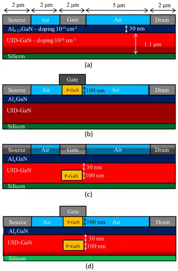
2 µm Drain Silicon UID-GaN – doping 1016 cm-3 1.1 µm 2 µm Gate Source 2 µm 5 µm 2 µm Air Air Al0.25GaN – doping 1015 cm-3 30 nm Drain Silicon UID-GaN P-GaN
Source Air Air
AlxGaN
Drain
Silicon UID-GaN
Gate
Source Air Air
AlxGaN Gate (a) (b) (c) Drain Silicon UID-GaN P-GaN
Source Air Air
AlxGaN Gate (d) P-GaN P-GaN 30 nm 30 nm 100 nm 100 nm 100 nm 100 nm
Hybrid normally-off AlGaN/GaN HEMT using GIT
technique with a p-region below the channel
Saleem Hamady
1,2,4, Frédéric Morancho
1,3, Bilal Beydoun
4, Patrick Austin
1,3, Mathieu Gavelle
1,21
CNRS, LAAS, 7 avenue du Colonel Roche, F-31400 Toulouse, France
2Univ de Toulouse, LAAS, F-31400 Toulouse, France 3Univ de Toulouse, UPS, LAAS, F-31400 Toulouse, France 4GET/LPE, Lebanese University, Hadath campus, Beirut, Lebanon
E-Mail: shamady@laas.fr, morancho@laas.fr, bilbey@ul.edu.lb, austin@laas.fr, mathieugavelle@yahoo.fr
Abstract— Gallium nitride based High Electron Mobility
Transistors (HEMT) are powerful candidates for high frequency and high power applications. Unfortunately, while switching applications demand normally-off operation, these devices are normally-on. In this paper, after calibrating the simulator using experimental data, we address the advantages and drawbacks of two normally-off HEMT devices: the previously proposed Gate Injection Transistor (GIT) and our newly proposed HEMT with a p-GaN region below the channel. Afterwards, an hybrid normally-off HEMT is proposed, combining both techniques, aiming to merge their advantages and remedying their drawbacks.
I. INTRODUCTION
GaN HEMT seems to be a very promising candidate for future power applications. Thanks to the GaN properties and the HEMT’s topology, AlGaN/GaN HEMTs are now potential candidates for high frequency applications with high power and low noise, such as microwave and millimeter wave communications, imaging and radars. While power switching applications strongly demand normally-off operation [1], conventional HEMTs are normally-on. Several normally-off structures have been proposed such as recessed gate structure [2], fluorine ion treatment device [3] and Gate Injection Transistor (GIT) [4].
II. SIMULATION STRATEGY
In this work, we will start by simulating two normally-off HEMTs: HEMT with a p-GaN region directly below the gate (gate injection transistor - GIT) (figure 1b) and our newly proposed HEMT with a p-GaN region below the AlGaN/GaN interface (figure 1c). After pointing the advantages and drawbacks of these structures, a new design combining the two techniques (two p-GaN regions: one below the channel and another above it) (figure 1c) is studied. All the device parameters remain constant throughout the simulation, except for the doping concentration and the position of the p-GaN region. To do this study, ATLAS, a physically-based TCAD simulation tool from Silvaco is used. Physical models used in the simulation include Shockley-Read Hall recombination, Fermi-Dirac statistics and field-dependent mobility. The simulator was calibrated by using real parameters of a normally-on HEMT device.
Figure 1. Schematic cross section of the (a) conventional HEMT used for calibration, (b) GIT transistor, (c) our proposed HEMT with a p-GaN region
below the channel and (d) GIT with p-GaN region below the gate. IN THE 3 FIGURES, YOU SHOULD REPLACE “SILICON” BY
“TRANSITION LAYERS / SILICON”
III. RESULTS AND DISCUSSION
Figure 2 shows the simulated transfer characteristics of the conventional normally-on HEMT and GIT both with x-mole fraction of 0.15. In the GIT, two different p-doping concentrations were used: 1018 cm-3 and 4×1018 cm-3. The thickness and the width of the p-GaN region is 100 nm and
0 0.01 0.02 0.03 0.04 0.05 0.06 ‐2 ‐1 0 1 2 3 4 5 C u rr e n t (A /m m ) Gate to Source Voltage Vgs(V) Drain to Source Current ‐ Hybrid structure Gate current ‐ Hybrid structure Drain Current ‐ Conventional HEMT Gate Current ‐ Conventional HEMT 0 0.002 0.004 0.006 -2 -1 0 1 2 3 4 Cu rr e n t (A /m m ) Ga te to Source volta ge Vgs(V)
Gate Current - P-region below the channel Drain Current - P-region below the channel Gate Current - Conventional HEMT Drain Current - Conventional HEMT
0 0.002 0.004 0.006 0.008 0.01 ‐8 ‐6 ‐4 ‐2 0 2 4 6 8 C u rr en t (A /m m ) Gate to source voltage Vgs(V) Gate Current ‐ GIT p‐doping = 4 ×10¹⁸ cmˉ³ Drain Current ‐ GIT p‐doping = 4 ×10¹⁸ cmˉ³ Gate Current ‐ GIT p‐doping = 10¹⁸ cmˉ³ Drain Current ‐ GIT p‐doping = 10¹⁸ cmˉ³ Gate Current ‐ Conventional HEMT Drain Current ‐ Conventional HEMT
1 μm respectively. It can be seen that the introduced p-GaN region, above the AlGaN layer, increases the threshold voltage. Moreover, the shift in the threshold voltage increases with increasing the doping concentration. At a doping concentration of 4×1018 cm-3, the threshold voltage increases from -1.1 V to 0.6 V as well as the forward gate voltage which increases from 3.2 V to 7 V.
Figure 2. Simulated transfer characteristics of the conventional
normally-on HEMT and GIT with p-GaN doping cnormally-oncentratinormally-ons of 1018 cm-3
and 4×10¹⁸
cm-3.
Figure 3. Simulated transfer characteristics of the conventional normally-on HEMT and HEMT with a p-GaN reginormally-on below the channel. The p-doping
concentration is 1018 cm-3.
Figure 3 shows the simulated transfer characteristics of the conventional normally-on HEMT and HEMT with a p-GaN region below the channel. The x-mole fraction in the two structures is equal to 0.15. The doping concentration, thickness and width of the p-GaN region are 1018 cm-3, 100 nm and 1 μm respectively. The distance between the p-GaN region and the AlGaN/GaN interface is equal to 30 nm. It can be seen that the introduced p-GaN region below the channel increases the threshold voltage from -2 V to 0.6 V. However, it decreases the forward gate voltage from 3.2 V to 0.9 V.
It is clear from figures 2 and 3 that although the same threshold voltage (0.6 V) was achieved after introducing the p-GaN region, the doping concentration required to achieve this threshold voltage is lower (1018< 4× 1018 cm-3) when the
p-GaN region is introduced below the channel rather than above it. On the other hand, the forward gate voltage is much higher when the p-GaN region is introduced above the channel. To achieve normally-off HEMT with relatively low p-doping concentrations and high forward voltage, a design combining the above mentioned techniques is proposed. Figure 4 shows the simulated transfer characteristics of an hybrid normally-off HEMT, with a threshold voltage of 2.5 V and a forward gate voltage of 3.8 V, using the GIT technique with a p-region below the channel. The doping concentration, thickness andwidth of the p-GaN region are 5×1017 cm-3, 100 nm and 1 μm respectively. The distance between the p-GaN region and the AlGaN/GaN interface is 30 nm.
Figure 4. Simulated transfer characteristics of the conventional normally-on HEMT and the hybrid normally-off HEMT with a p-doping
concentration of 5×1017 cm-3.
IV. CONCULUSION
In this work, we address an advantage and a drawback of the two normally-off HEMT devices: the previously proposed Gate Injection Transistor (GIT) and our newly proposed HEMT with p-GaN region below the channel. Simulation results have shown that the doping concentration required to achieve the desired threshold voltage is lower when the p-GaN region is introduced below the channel rather than above it. On the other hand, the forward gate voltage is much higher when the p-GaN region is introduced above the channel. To achieve a normally-off HEMT with high forward gate voltage, using a relatively low p-doping concentration, an hybrid normally-off HEMT was proposed using two p-GaN regions, one above the channel and another below it.
REFERENCES
[1] H. Kambayashi, Y. Satoh, T. Kokawa, N. Ikeda, T. Nomura, and S.
Kato, “High field-effect mobility normally-off AlGaN/GaN hybrid MOS-HFET on Si substrate by selective area growth technique,”
Solid-State Electron., vol. 56, no. 1, pp. 163–167, Feb. 2011.
[2] S. D. Burnham, K. Boutros, P. Hashimoto, C. Butler, D. W. S. Wong,
M. Hu, and M. Micovic, “Gate-recessed normally-off GaN-on- Si HEMT using a new O2-BCl3 digital etching technique,” Phys. Status
Solidi C, vol. 7, no. 7–8, pp. 2010–2012, 2010.
[3] H. Chen, M. Wang, and K. J. Chen, “Self-aligned enhancement-mode
AlGaN/GaN HEMTs using 25 keV fluorine ion implantation,” in
Device Research Conference (DRC), 2010, 2010, pp. 137–138.
[4] Y. Uemoto et al , “Gate Injection Transistor (GIT) - A Normally-Off
AlGaN/GaN Power Transistor Using Conductivity Modulation,” IEEE