ACTt'
RC
NETWORKS
DOCUMENT ROOMACi T. OOM136-412
RESFARCH LABORAT' RY OF EFCTRO[NI1CHA D D. THORNTON IfASSACHUSETT`S INSTI.UTE OF TECHNOLOGY
CAMBRID 39, MASACHUSETTS, U S.A.
TECHNICAL REPORT 334 May 15, 1957
RESEARCH LABORATORY OF ELECTRONICS MASSACHUSETTS INSTITUTE OF TECHNOLOGY
CAMBRIDGE, MASSACHUSETTS
The Research Laboratory of Electronics is an interdepartmental laboratory of the Department of Electrical Engineering and the Depart-ment of Physics.
The research reported in this document was made possible in part by support extended the Massachusetts Institute of Technology, Research Laboratory of Electronics, jointly by the U. S. Army (Signal Corps), the U. S. Navy (Office of Naval Research), and the U. S. Air Force (Office of Scientific Research, Air Research and Development Command), under Signal Corps Contract DA36-039-sc-64637, Department of the Army Task 3-99-06-1.08 and Project 3-99-00-100.
Active RC Networks*
RICHARD D. THORNTONt
INTRODUCTION
ET US assume that all devices that are available
dL
1
j for circuit synthesis can be approximated bylinear models with lumped, terminal, capacitive, energy storage, but otherwise arbitrary, resistive character-,istics. An example of a four-terminal device of this class is shown in Fig. 1. If we combine a number of these devices with an ideal transformer network, we can con-struct an active RC network, but the characteristics of the available devices impose constraints on the natural
* Manuscript received by the PGCT, May 15, 1957. This work was supported in part by the U. S. Army (Signal Corps), the U. S. Air Force (Office of Sci. Res., Air Res. and Dev. Corn.), and the U. S. Navy (Office of Naval Research).
t Dept. of Elec. Eng. and the Res. Lab. of Electronics, Mass. Inst. Tech., Cambridge, Mass.
frequencies of such a network. This paper determines the bound on allowed natural frequencies in terms of the eigenvalues of a frequency matrix and relates them to the maximum power that can be dissipated by the device per
unit energy stored in the terminal capacity. Examples are given to indicate the relation between the gain-bandwidth product and the allowed natural frequencies, and the design of a nonunilateral constant-h amplifier is considered.
RIEPRESENTATION OF DEVICE C.IIARAtCTI;IRISICS
An n + 1 terminal linear device, of the type shown in Fig. 1, can be completely described by a conductance and a capacitance matrix
Thornton: Active RC Networks [G] is arbitrary real; [C] is symmetric, real, positive definite.
The G matrix will have n2 real elements and the C matrix will have n(n + 1)/2 distinct real elements; thus a total of n(3n + 1)/2 distinct parameters will be needed to describe the device. In order to simplify calculations, it is expedient to reduce the device to a canonic form that requires the fewest number of parameters to completely describe the device. In particular, we can imbed the original device in a transformer network and create a "new" device that is described by
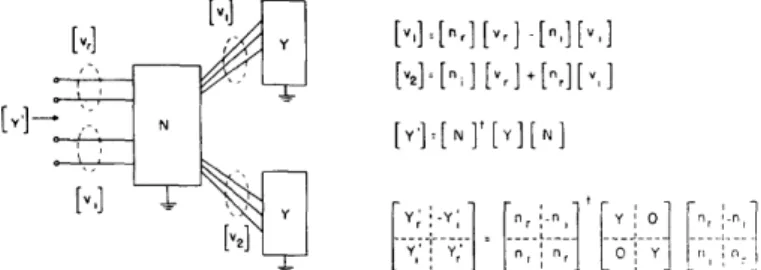
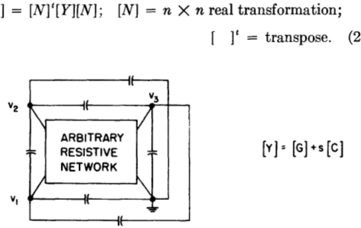
[Y'] = [N]t[Y][N]; [N] = n X n real transformation; I ]' = transpose. (2)
S11 812 -S31 [S] = -812 S22 823 831 -823 S33 _
(4)
The circuit interpretation of this matrix is shown in Fig. 2. It is seen that the canonic form of an (n + l)-terminal device is n-parallel GC circuits, with gyrator coupling between each pair of GC circuits. Moreover, the elements of [S] are seen to be invariant to imbedding a single device in a transformer network, and hence might be called "frequency invariants."
V2 4
VI
Fig. 1-Device with capacitive, terminal energy storage.
A classical theorem of matrix algebra states that it is always possible to find a transformation of this sort which simultaneously diagonalizes two real matrices, provided that they are both symmetric and one of them is positive definite. It is therefore possible to diagonalize the symmetric part of G and C simultaneously, and since C is positive definite, we can always find an [N] that reduces [Y'] to the form:
S33
[Y]: [G]+s[C]
Fig. 2-Circuit interpretation of canonic form.
As a simple example of this reduction of a device to canonic form, consider the three-terminal device described by
[Y] = 1 912 +
921 L g,, 922_!12 g,,JLc 1, C c2212.J
(5)
The procedure for finding the Smatrix and the appropriate transformation IN] can be given in cookbook style as follows.
1) Compute the symmetric part of the conductance matrix and the inverse of the capacitance matrix. [Y'] = ([S] + s[I]) Co (3)
[S] = n X n real, antisymmetric matrix [I] = identity matrix; C = real constant. [S] will be called the "frequency matrix," because the elements of this matrix have the dimensions of frequency. We see that if Co is of unit value, a knowledge of IS] is sufficient to completely describe the device.
The inverse transformation can always be utilized to reconvert [Y'] to [Y], so that, if we allow the use of ideal transformers for network synthesis, the frequency matrix offers a complete description of the device and requires only n(n + 1)/2 distinct parameters. Since there are only n2 elements in the transformation [N], we see that it is impossible to describe the device by fewer than n(n + 1)/2 and that [S] offers as simple a representation as is possible. Admittedly, if ideal transformers are not allowed, the frequency matrix does not offer a complete description of the device, but in this paper we are primarily interested in bounds on the behavior of a network and thus we allow the use of transformers.
The S matrix for a four-terminal device will be
,
2g + 921 [G,] [G] + [G]' =F
22
912 + 9212
922 [C , Cl 1F
c22 C12.
Cl-C22 I 1 2_ C1 [ _C12 ell1 (6)2) Form the product [G,][C]-' and determine the eigenvalues of this product matrix. These eigenvalues are the diagonal elements of the frequency matrix.
(7) [G.][C]-1 [ a b
c d
EV = + -~4 2 + bc.
[- d 2 i
3) Working backwards, we can use the expression [N]-'"([S,] + s[I])[N]-'Co = [Ga] + s[C] to compute the matrix [N]-'.
V3 11 ARBITRARY RESISTIVE NETWORK
/-"
l , 11~~~\
1957 79 11Z
IRE TRANSACTIONS ON CIRCUIT THEORY [N]- = In n::1 n21 n22 2 ni2 = (ClS2 2 - 11)/(S22 - s)Co 2 n2 = (C2 2S22 - 92 2)/( 2 2 - 82)Co n2 = (CS11 - gll)/(s11 - S2 2)Co (8) n22 = (C22S1 - 2 2)/(Sll - S22)CO (nllnl2 + n2 2n2 )Co = C1 2.
The equation containing c,2 is used only to determine the
signs of the n's and is always satisfied if the s,, and s22 are correctly computed.
4) We can then compute [N], and from the original relation, [N]t[G][N] = [S], we can determine the anti-symmetric components of the frequency matrix. For a 2 X 2 matrix, however, the nondiagonal elements of the S matrix can be found from the relation
S 21 S21 = EV([Ga][C]-1 ) 0 912 - 921 [G - []' 2' [G = [G] - ] 22 -- g912 + 921
2jAs a assumenumerical example, let us
As a numerical example, let us assume
[Y] =
/5
-
\5
1+
1j
+
2-J3
If we define a natural frequency as that frequency at which it is possible to excite the circuit without the necessity of supplying driving power, we can determine the allowed natural frequencies without great difficulty. The power dissipated by a network' is
P = V]t[Y(s)][V] = [V]t([S] + s [I])[V]Co
= complex power at frequency s; [V] = complex voltage column matrix;
[V]t = transposed conjugate of [V]. (13) To determine the allowed natural frequencies, we need only find those values of s for which a voltage matrix can be found that satisfies the relation P = 0. The details of the solution to this problem are given in Appendix I, but the answer is relatively simple. If we define a matrix [SB] as
I[S] = [S]e-i - [S]'te'
2j
[S] [S]sin 0 [S] - S] cos0,
-2 2j (14)
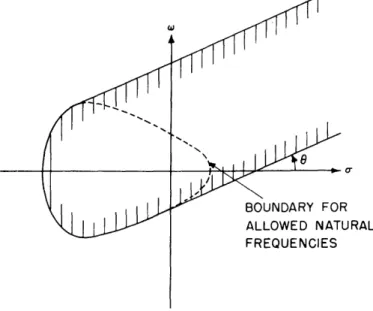
the bounds on the allowed natural frequencies can be determined from the maximum eigenvalue of S, EVM [SE], by a relatively simple geometrical construction. For each value of 0 we compute EVM[S,] and perform the construction indicated in Fig. 3. The envelope of the lines (10) w cos 0 - sin = EVM[So] is the desired boundary.
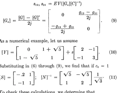
Substituting in (6) through (9), we find that if c = 1
[S]= [ 2 1j; [N]-'5 (11)
To check these calculations, we determine that
[N]-'t[S][N]-' = [G]; [N]-''t[N]- 1 = [C]. (12) The only real justification for this elaborate procedure is that we can now easily compare two devices, and hence future calculations are greatly simplified. Our
synthesis procedure will then consist of three steps: 1) Convert the available device into a canonic form described by [S].
2) Synthesize the desired circuit in canonic form. 3) Reconstruct the exact desired circuit by means of the appropriate transformer network.
ALLOWED NATURAL FREQUENCIES
Before discussing actual synthesis procedures, let us determine the allowed natural frequencies of a circuit. If the available devices have inherent terminal shunt capacity, there will be definite restrictions on the natural frequencies that may be realized, and these can be ex-pressed entirely in terms of the characteristics of the device without reference to the manner in which the device is to be used.
= EVM [So]
so] [[s]5e. - [s] ]
2 Jr
Fig. 3-Graphical determination of allowed frequency bound.
If we had asked the question, "For what values of s can we dissipate a complex power P = P I e'?," the answer could be determined by the graphical construction shown in Fig. 4. The magnitude of the power dissipated can always be increased merely by increasing the magni-tude of the driving voltages, but there are definite con-straints on the phase angle at which power can be dis-sipated. The constructions of Fig. 3 indicate that, once we know EVM[So] for all values of 0, it is possible to determine all of the bounds on the allowed power
dis-1 The justification for this definition of power, and its interpre-tation for more complex systems, will be discussed in a future paper. For the present, however, we shall merely assume this definition of power and consider the consequences.
September 80
Thornton: Active RC Networks
frequencies is equivalent to the determination of the maximum power/energy ratio and gives us a time-domain interpretation of the allowed natural frequencies; the allowed X are the negative of the allowed s. This interpretation will prove useful presently in discussing amplifier limitations.
According to the previously assumed definition of complex power, we see that a gyrator described by an antisymmetric matrix,
O'
R U RAL
Fig. 4-Bounds on dissipation with a power angle 0.
sipation; hence these eignvalues tell us a good deal about the characteristics of the device.
Suppose that instead of calculating the allowed natural frequencies, we had asked the question, "What is the maximum complex power that can be dissipated in the resistive part of the device per unit energy stored in the terminal capacity." If such a maximum exists, it will certainly constitute a limitation on network behavior, because a network composed of a collection of devices plus ideal transformers cannot dissipate more power per unit stored energy than the devices themselves; therefore this maximum power/energy ratio must be an invariant property of the device. It should be understood that we must specify the phase angle of the power we are trying to dissipate and the determination of this maximum power/energy ratio will be a function of the power angle. The power dissipated and the energy stored2 are given by
[V'[G]l[V]= [v']'[S][V'] C
complex resistive power dissipation (15) [v]y[C][Vllj = v'][Il'] Co,
= twice the capacitive stored energy. If we define X as the ratio of power dissipated to twice the energy stored, we see that
[V']'[GI[V']
[vT[V'] (16)
[Vw]'([s] - x[I)[v] = o.
It is readily seen that (16) is identical with the require-ment that the total power P be zero at a frequency s = -X. Thus the determination of allowed natural
2 The usual representation of complex quantities would require that the energy and power of (15) be average values. It is possible, however, to find an interpretation for which these are instantaneous values. This idea will be discussed in the paper mentioned in
foot-note .
gyrator matrix = [0 G
-G
is a device that dissipates imaginary power, while a resistor is a device that dissipates real power. The ex-pression "dissipation of imaginary power" might appear to be somewhat strange but, since both real and imaginary power are conserved, there is nothing unreasonable about it. It is, in fact, this conservation of imaginary power that imposes some very important restrictions on network behavior, but this is beyond the scope of the present paper. We can see that imaginary power dissipated by a gyrator is nothing more than the power transmitted through the gyrator when two batteries are connected to two terminal pairs of the gyrator. The direction of power flow depends only on the direction of the gyrator arrow and on the polarity of the exciting voltages and not on the magnitude of the two battery voltages. For a low-gain amplifier, the power transmitted through the amplifier may be greater than the actual power supplied by the amplifier, so it is reasonable to expect that imaginary power is an important quantity for amplifier analysis.
Some typical plots of allowed natural frequencies are shown in Figs. 5-7. Note, in particular, that, for a three-terminal device, the frequency matrix can be written in the form
iS]
r
-0. 1L
-c t O .2 ]It can be readily shown that the allowed natural fre-quencies for any three-terminal device are contained within an ellipse, and the bounds on this ellipse in the
complex plane are given directly by the three elements of the S matrix, as indicated in Fig. 5. This characteristic' ellipse has some interesting properties and affords a simple and interesting way of describing a device. Some of its properties which can be determined directly from the characteristic ellipse are:
1) The foci are the open-circuit natural frequencies of the device; thus the stability of the device is ensured if both focuses are in the left half-plane.
The natural frequencies are
l + Oa zh <(0. - 2 )2 -( 2 sl, s2 --
2
4-
+
2
-
WI.
(19)
w (17) Oi _ 0'2. 81 1957IRE TRANSACTIONS ON CIRCUIT THEORY
3) The maximum frequency of sinusoidal oscillation is given by the intersection of the ellipse with the a = 0 axis; thus it is given by
= - + a2) 1/2
amwl - 02
Fig. 5-Characteristic ellipse of three-terminal device. C
-WI
Fig. 6-Allowed frequencies for a four-termina]
co
Under no condition can this frequency, Cm,, be exceeded
if inductors are not allowed for circuit synthesis.
4) All exponentially growing waveforms must have time constants within the range
-1' < < al'
If ideal resistors are available, the lower limit is minus infinity but under no condition can a time constant exceed ao-'.
li
01
If the device has four terminals with four nondiagonal ]-,-2 o zeros, the allowed natural frequencies are as shown in0 0 -3 Fig. 6. This device may be thought of as one three-terminal
device plus a separate two-terminal device with G/C ratio of -a,, but we shall treat it as though it were a single device. In the limit as a, approaches minus infinity we can think of this device as the previously discussed I device. three-terminal device plus an ideal resistor; thus it is a simple matter to include the use of resistors in circuit svnth i .
I'
---o
0 We have established necessary bounds on allowedo
0 natural frequencies, but we must still show that these are|-1 I also sufficient conditions. The sufficiency is best established
>1 -I by a direct synthesis procedure, which is given in Appendix
II. The canonic form of a maximum-frequency oscillator is a three-terminal device with
[S] =
[~:
"'} ,natural frequencies = al-, jw,. (23) - co _ a0a
The characteristic ellipse of this device is the degenerate case of a vertical line in the splane, with end points
= al t- jl. -I
SYNTHESIS OF THREE-TERMINAL DEVICES
Fig. 7-Synthesis of a "pentode."
unilateral power gain of the device is given
U 2
U - L2 (20)
and thus it is invariant to imbedding the device in a transformer network, as has been shown by Mason.3
aS. J. Mason, "Power gain in feedback amplifiers," M.I.T. Res. Lab. of Electronics, Tech. Rep. 257; August 25, 1953; also, IRE TRANS., vol. CT-1, pp. 20-25; June, 1954.
Let us now consider the problem of synthesizing a desired three-terminal device from an available multi-terminal device. (There is only a verbal distinction between a "device" and a "circuit" so we shall, for convenience, always refer to device synthesis.) Let us use the symbol Da to represent an available device whose frequency matrix is known, and use the symbol Dd to represent a device whose characteristics are specified and which we are trying to synthesize by combining available devices in a transformer network. The circuit synthesis question might be "Can Dd be synthesized from Da and, if so, how?" or it might be expressed "If the elements of the frequency matrix describing Dd are specified within a constant multiplier, what is the largest possible value of this constant multiplier?" Thus for a three-terminal Dd
(21) Do 03 _I (22) -I 2) The dc by September 82 F E
:=,,f
/2
Irl WI 01 N = I-, --, Ir-I
Thornton: Active RC Networks we might ask, "If the center and the aspect ratio of the
ellipse are fixed, what is the largest possible area for the ellipse?"
It should be recognized immediately that the region of allowed natural frequencies for Dd must lie entirely within the region of allowed frequencies for Da or else there is no hope of synthesizing Dd. To word this dif-ferently, if we cannot dissipate more than 2X watts per unit energy stored in the original device, then we cannot expect to dissipate more than 2X watts per unit energy stored in the "new" device. We see that this bound on allowed natural frequencies is a necessary condition that must be satisfied, but it is not, in general, a sufficient condition for realizability. It is true, however, that for the special case when both Dd and Da are three-terminal devices, the bound on allowed natural frequencies is both a necessary and sufficient limitation. This fact is best demonstrated by a direct synthesis procedure.
If [S]a is the 2 X 2 frequency matrix of the available device, we can construct a "new" device by combining two available devices in the following way:
resistor (either with or without some capacity in shunt with the resistor). It is thus possible to synthesize the matrix [Sd] from [SJ, as shown in Fig. 6.
In general it is not possible to synthesize any three-terminal device that is limited only by the constraint that its characteristic ellipse lies interior to the allowed region of natural frequencies. Thus, for the five-terminal device with a frequency matrix, as shown in Fig. 7, the largest possible characteristic circle, centered at the origin, that can be synthesized, has a radius of x = 2-1/2 = 0.707.
The appropriate synthesis procedure that realizes this radius is given by [Sd] = [Ni]'[Sa][N1] /[s 2 -[ _ -1_ [I] = [N,]'[N,] a 0 [N.] = b O -c d O_ [Sd] =[Al]'[Sal[A] + [N2][Sa] [[N 2]; [N2]'[N] + [N2]'[N2] = [I]
o0[a
] NbFOd
-c] a2 + 2 = 1 bjLd
b2 + C2 = 1 (25) (24) a =+ 2]1/ 2 a =c = L 4 -aa - d2f2 (ab + cd)cw,- (ab + cd)o, -b2a - c2a,
Elementary algebraic manipulation shows that the Dd so constructed has a characteristic ellipse interior and just tangent to the characteristic ellipse of Da. Since the frequency invariants of the new device will, in general, be different from the frequency invariants of Da, we see that the synthesis could not be accomplished with a single device and, since 2 comes after 1, two devices must be the minimal number. We might thus describe the above synthesis technique as optimal, since it synthesizes the "best" possible Dd with fewest possible number of Da's.
It is possible to synthesize a device whose characteristic ellipse is interior but not tangent to the ellipse of Da,
but, since we are only interested in determining limi-tations, this more general procedure will not be given. In a practical situation it is usually best to use passive resistors and capacitors as shunt elements to reduce the size of the characteristic ellipse, since these passive elements are normally stable and reliable.
Another situation in which the allowed frequency bound is a necessary and sufficient limitation arises with devices of the type shown in Fig. 6. The technique for accomplishing this synthesis is explained in Appendix III. This four-terminal device is particularly important, since it is equivalent to a three-terminal device plus a
b = d = [ 2-
]/2
1The general problem of three-terminal synthesis has not been solved, but it has been possible to establish lower bounds, as well as upper bounds. If we construct two maximum-frequency oscillators, by the technique described in Appendix II, and if one of these oscillators has natural frequencies on the w = 0 axis, we can always synthesize a device limited by the lower bound shown in Fig. 8. The synthesis procedure for this lower bound has already been discussed (see Fig. 6). It is seen that this lower bound is never much worse than the upper bound and thus the determination of allowed natural frequencies gives us a good, if not exact, idea of the kind of three-terminal device that may be synthesized.
Synthesis of devices with more than three terminals has not been attempted. It appears, however, that the' optimum synthesis can always be carried out by simple transformations of the canonic form, in a manner similar to that described for three-terminal devices. The fact that the optimum synthesis can be expressed by a simple transformation of the [S] matrix partially justifies the effort of converting the original device to canonic form.
WIDE-BAND AMPLIFIER SYNTHESIS
Let us now apply some of the preceding ideas to the design of wide-band amplifiers. As a first example, we might consider the design of a unilateral amplifier with
1957 83
I I 0 is. =
IRE TRANSACTIONS ON CIRCUIT THEORY
6
BOUND BOUND
.a
Fig. 8-Upper and lower bounds on allowed frequencies.
u"/ 2W
ESISTOR
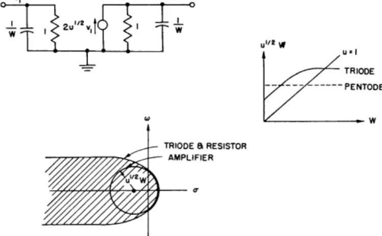
equal input and output admittances and a matched unilateral power gain U, as shown in Fig. 9. The character-istic ellipse for this circuit is a circle centered at the frequency s = -W = -G/C, where W is the half-power bandwidth i'or a single stage (with voltage excitation). The radius of this circle is the voltage gain-bandwidth product; thus we see that the gain-bandwidth product is related to the area of the allowed region of natural fre-quencies for the available devices.
If we attempt to build this amplifier by utilizing a vacuum triode, we must first determine the frequency matrix for a triode. If a triode is approximated by
y] = 0
]
+- C' [Y] = + S gm gm/ t -C m Cp we find that [S] = - 1i -1 -2 gm/2 0' = C + [C2 + C 2 w = g./2C2 0'2 = CgCp - Cm > o, gm/2Fig. 9-Synthesis of a unilateral amplifier from triodes.
where
C1 = (C/,) + Cm; C = CC' - Cm.
The frequency invariants for some typical high-fre-quency receiving tubes are given in Table I. A knowledge of these invariants, for the tube to be used in circuit synthesis, enables us to dimension the gain-bandwidth product vs bandwidth plot shown in Fig. 9. We must then decide on a compromise between gain and bandwidth, and design the amplifier by previously discussed tech-niques. The final circuit might be similar to the circuit shown in Fig. 13.
As a second example, let us construct an amplifier with a flat frequency response and with maximum gain. The iterated gain of one stage of amplification can be found by assuming that the admittance that loads this stage is equal to the input admittance. We find that the iterated voltage gain is given by
C1 - [C2 + C2]1 2
W = gm/2[CC] 2,
Y21
Yo ±-
V/Yo
- Y12Y21 ; Yo = (Y11 + Y22)/2
. (27)
TABLE I*
FREQUENCY INVARIANTS FOR TYPICAL VACUUM TUBES
Bias Circuit Parameters Invariants
eb ec2 ib Co - Cm Cp- Cm Cm .m m 0-1 0'2 W1
tzuf , f Uuf M X 109 sec
-Triodes 6AF4A 80v 28 ma 2.2 0.45 1.9 10 17 0.92 -4.3 2.0 6AJ4 125v 18ma 4.4 0.18 2.4 11 44 0.80 -3.2 1.6 6BK7A 150v 18 ma 3.0 1.0 1.3 9.3 43 0.83 -2.6 1.5 Pentodes 6AH6 150v 150v 22 ma 10.0 2.0 0.03 6.4 > 1000 0.98 -0.95 0.94 6AK5 120v 120v 14 ma 4.0 2.1 0.03 7.5 > 1000 1.29 -1.31 1.30 6CB6 150v 150v 14 ma 6.5 2.0 0.02 7.5 > 1000 1.04 -1.06 1.05 6CL6 150v 150v 50 ma 11 5.5 0.12 12 500 0.81 -0.83 0.82
* For all tubes except the 6AJ4 all electrodes except the control grid and plate are incrementally grounded. For the 6AJ4, the heater is connected to the grid. Biases are chosen for best performance within the current and dissipation limits of the tube.
September 84
Thornton: Active RC Networks If we now construct an amplifier stage with the admittance
matrix
[Y] =
SC
g]
1
- g sC gfg, = G2 g,gr = K G/C = W, we see that the iterated gain of this stage is given byK1/2
K, =
(s/w) +
/(soff)
2+ 1
This expression is recognized to be similar to the ex-pression for the gain of an iterated LC ladder network and is also similar to the frequency response derived by Bode4 for an optimally flat amplifier. However, the amplifier described above differs in two respects: 1) This amplifier has a voltage gain per stage of K'/ 2 which can be made greater than unity, unlike the LC structure, and 2) for an iterated network, no infinitely complicated coupling network is needed to realize this response. Eq. (29) stipulates that I K, i = K12 for s = jw, w < W, and K, has a constant 900 phase shift for frequencies greater than W.
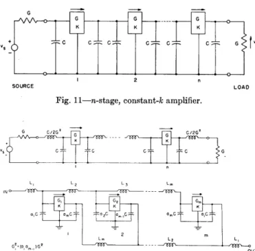
The characteristic ellipse for this amplifier stage is given in Fig. 10. It is immediately seen that the band-width and power gain are incompatible if the area of the characteristic ellipse is restricted to some allowed region. For a high-gain stage we would like the ellipse to be nearly a circle but, since the bandwidth is the distance from either of the focuses to the origin, we must have a long thin ellipse for a wideband stage. Note, in particular, that the bandwidth can never exceed wm = maximum frequency of sinusoidal oscillation of the available device. In the limit as W approaches cwm the gain K approaches unity and we have a very definite limit on available bandwidth. An n-stage amplifier with the constant-k frequency response is shown in Fig. 11, with the source and load chosen for maximum available power gain. The box with a G and a K inside it is used to designate the device shown in Fig. 10. We could use a more sophisticated matching network' at each end of this filter, but a reasonably good response can be obtained with a single-resistor termi-nation. The over-all power gain of this n-stage amplifier is Knand can always be increased while a constant band-width is maintained, limited only by W < cw.
If we now add an inductor of value L = C/G2 between each stage of the amplifier, we can double the bandwidth at the expense of increasing the phase shift for frequencies greater than W. Note that this doubling of the bandwidth
4H. W. Bode, "Network Analysis and Feedback Amplifier Design," D. Van Nostrand Co., Inc., New York, N.Y., pp. 409-410; 1945.
5 It. M. Fano, "Theoretical limitations on the broadband match-ing of an arbitrary impedance," J. Franklin Inst., vol. 249, pp. 57-83; January, 1950, and pp. 139-154; February, 1950.
H. J. Carlin and R. LaRosa, "Broadband reflectionless matching with minimum insertion loss," Proc. Symposium on Modern Network
Synthesis, Polytechnic Inst. of Brooklyn, pp. 161-178; April 16-18,
1952.
Fig. 10-Characteristic ellipse of a one-stage, constant-k amplifier.
Vs
SOURCE
Fig. 11-n-stage, constant-k amplifier.
G C/2G C/2G
S C C C C S G
LOAD
L3 Lm
Fig. 12-Inductor-compensated and distributed
amplifiers.
OUT
constant-k
is similar to the increase derived by Bode6for an infinitely complicated series interstage network. The only apparent disadvantage of the present scheme is that the over-all amplifier is nonunilateral, but it is not obvious that this is any disadvantage. For example, if we were to construct the mechanical analogue of this constant-k amplifier, we would have a useful force-reflecting system. The driving force could "feel" the load directly, only the magnitude. of the forces would be altered by the amplifier.
If we must have a bandwidth greater than 2w,, we can resort to a distributed structure, as shown in Fig. 12. If' we use m stages in parallel, we find that the ratio of the bandwidth for m stages to the bandwidth for a single stage, F(m), is as given in Table II. In the limit as the number of stages becomes large the bandwidth is always greater than, but approximately equal to,
F(m) m/7r for m large.
6 Bode, op. cit., pp. 427-431.
(28) FOCUS (29) -2 G = [-9, sC G' 9, 9 g K 9,/9r 1957 85 I'l q-IN u1 [uiu mr I
IRE TRANSACTIONS ON CIRCUIT THEORY TABLE II
CIRCUIT VALUES FOR FIG. 12
4C Li-= 2 2 F2G2ai m F(m) al a2 a3 a4 1 1.000 1.000 2 1.414 1.000 0.500 3 1.802 1.000 0.692 0.308 4 2.175 1.000 0.789 0.500 0.211
~ large m/r ai = cos 7ri2/2m 1 << i << m
It would thus require about 30 stages to increase the band-width by a factor of 10. The gain for this 30-stage dis-tributed amplifier would be only K; thus it is doubtful that this type of circuit has much practical value. It does illustrate, however, that the bandwidth and gain can both be increased without limit if we are willing to use enough amplifier stages with inductor interstage networks. The individual amplifier stages, for either the uni-lateral amplifier or the constant-k amplifier, would look something like the circuit of Fig. 13 for a synthesis utilizing triodes. The input and output are both coupled to the grids and plates of both tubes. The amplifier is thus neither grounded-grid, grounded-cathode, or anything else, but is designed to have a prescribed conductance matrix with minimum shunt capacity. In some special cases, the synthesis can be accomplished with one tube and one capacitor as, for example, in the construction of a unilateral amplifier from a triode. The capacitor serves a function similar to that of the neutralizing capacitor used frequently in RF amplifiers. In our synthesis, how-ever, the capacitor and feedback transformer are carefully chosen to maximize the gain-bandwidth product, and for low-gain stages we may not require any capacitor at all.
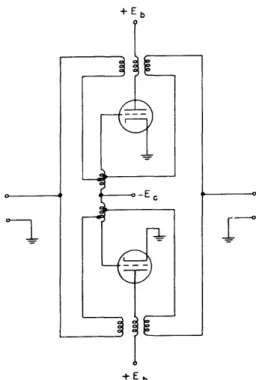
As a partial answer to critics who might consider our synthesis impractical, it might be well to indicate a possible method of constructing a constant-k amplifier without resort to transformers. The push-pull circuit of Fig. 14 has an approximate constant-k frequency response and comes surprisingly close to achieving optimum performance. For K = 1 and C, = C, this circuit is .optimum. Unfortunately, the synthesis requires four tubes per stage with two forward amplifying tubes and two reverse amplifying tubes. The forward and reverse 'tubes are biased differently so that there is a net gain in the forward direction; the gain bandwidth product of this amplifier is dependent only on the bias of the forward amplifying tube (i.e., the tube with the maximum g ).
The preceding discussion has made no attempt to present general synthesis techniques for amplifiers with prescribed transient response. The intent has been to demonstrate some relations between the characteristics of amplifiers and the allowed natural frequencies for the devices used to construct the amplifiers.
+Eb
+Eb
Fig. 13-Amplifier synthesis by using triodes.
Vf Vr ( ASSUME gp O) K 9 W= G Trflr C 4G2 grf gmr K'/2 W gmf/(Cg +Cp ) Vf Vr
Fig. 14-Push-pull realization of a constant-k amplifier.
CONCLUSION
This paper has attempted to formulate some of the limitations of devices that can be approximated by lumped, terminal, capacitive, energy-storage elements with arbitrary resistive characteristics. The synthesis assumes the use of ideal transformers and, although this may seem to be impractical, it enables us to determine the unavoidable limitations that cannot be overcome by any conceivable technique. Thus we have a yardstick with which to measure the performance of practical amplifiers. The general problem of synthesizing an arbitrary GC circuit from a variety of available amplifying devices has not been completely solved, but it is possible to establish both upper and lower bounds on the type of network that can be realized. The general problem of three-terminal synthesis has been considered, and it is shown that the characteristic ellipse offers a convenient measure of the performance of a device. We have also shown how three-terminal devices can be utilized to construct amplifiers with unilateral, single, time-constant response, and with nonunilateral, constant-k frequency response.
In particular, we have shown that the gain-bandwidth product has a definite interpretation in terms of allowed
1---11-- ' I---I----"r September 86
Thornton: Active RC Networks natural frequencies, but, in general, this product is not
an invariant property of a device. A determination of the allowed natural frequencies for an arbitrary device, and a consideration of the more general linear-amplifier synthesis problems will be given in a forthcoming paper.
APPENDIX I Problem
To prove that the region of allowed natural frequencies for devices with capacitive, terminal, energy storage is bounded by the graphical construction of Fig. 3, and that, for a power angle 0, the allowed frequencies are as shown in Fig. 4.
Proof
Assume that
[ V]'[Y][V] = = P = Pe' + jP2e', P, P, real. Then
[[V]'[Y][Vl]] = [] t[Y]'t[] = p* = Ple-i - jei' ,
[ ]' = conjugate transpose, P* = conjugate of P. After multiplying each of the expressions for P and P* by e-i and e, and solving for P, and P , we have
[V],[[Y]e- / + [Y]'e][ [V][Y6-, 2][V] = P
[]V[[YI]e' - [Y]e' ][V] [V]'[YO][V] = P2. If we can now force P2 to be zero, we can dissipate power at a phase angle 0. (Note, however, that the sign of P is not determined.) The condition that P = 0 is recognized as the condition that [Y] is neither positive definite nor negative definite. This will be true if and only if the eigenvalues of [Y0] and its principal minors are neither all positive nor all negative.
Substituting [S] + s[I] for [Y], we find that
[Y] [[ S ]e-i - [S] 'e _ (, cos 0 - o-sin ) [I]]
- [S] - x[].
Thus we see that, for P2 = 0, the allowed values of x = cos 0 -a sin are bounded by the maximum and minimum eigenvalues of [So] and its principal minors. If d = EVM[So] = maximum eigenvalue of S and its principal minors, we find that for x > d, P2 > 0. The lower bound on x is EVM[- Se], which may also be thought of as the upper bound for 0 increased by 180°. Thus only the maximum eigenvalue need be calculated.
Returning to the original expression for P,, we see that P =
[V] [S]e-" + [Sei- + (w cos 0 + a sin 0)[I] [V]
and, for the case shown in Fig. 10, with 0 < 0 < 7r/2,
P2 >0, P•O
P<O
P2'<0, P•O
P: P2 IS POSSIBLE Fig. 15-Construction for proof of Appendix I.
c and a become large positive, the foregoing expression for P, must become positive definite, while, for and a
large negative, P, must be negative definite.
Somewhere between these two extremes there must be a region in which P, is neither positive definite nor negative definite and in which it is always possible to force P = 0 and P2 = 0, simultaneously. We still do not know where
this region is, but it must exist, even though it is of infinitesimal width, and might appear as the shaded region of Fig. 15. Note, in particular, that this region must touch the bounds of x, which are determined by the eigenvalues of [So].
A simple geometrical construction indicates that the line x = d is a line, of slope tan 0, in the complex plane, and the distance from the line x = d to the origin is d. (The correct sign is easily determined by letting co or a = 0.)
Above the line x = d we must have P2 > 0, and hence P f 0, and no natural frequencies are possible. But we still do not know what the allowed region is; we only know that it touches the bound x = d and does not extend above the line x = d. If we assume different values of and plot all (or at least a large number) of the lines x = d(O), 0 < < 2r, we find that the allowed region of natural frequencies must lie inside of a closed convex curve bounded by the envelope of the equation x = d(8) or, alternatively, the envelope of the equation
o cos 0 - a sin 0 = EVM[So].
Within this region it is possible to dissipate power at any phase angle, while outside this region only certain' power angles are possible. We have already determined that dissipation at an angle 0 is only possible for fre-quencies lying between the parallel lines x = d(O) and x = d(O + 7r); the sign of P, remains to be determined. If P, could assume both positive and negative values outside the region of allowed natural frequencies, say for s = s, we could excite two circuits, one with P = +1 and one with P, = -1, and, by combining them, build a circuit with a natural frequency at s,. Since s is not
IRE TRANSACTIONS ON CIRCUIT THEORY allowed, however, this is an impossible situation, and
hence P1 must be either definitely positive or definitely negative, except in the region of allowed natural fre-quencies in which it may be either. Thus we see that the allowed frequencies for a power angle are those given in Fig. 4.
The appropriate [V] which causes [V]t[Y][V] = P = 0 can now be determined for any point on the boundary of the allowed natural frequencies. We construct a tangent line, as shown in Fig. 3, and form the matrix [So] for = angle between tangent and w = 0 axis. We then find IVM[S] and the corresponding eigenvector. This eigen-vector is the correct [V] to force P = 0.
° As an example, assume that
[] 1 -a 0w2
[ I] [,] [' ]-[ ] [ ]
[V,2] [ ] [ ,] i v, F+ ! F [Y ] -[ N] [ Y] [ N]
Fig.
16-Complex-admittance transformation.
Fig. 16-Complex-admittance transformation.
both necessary and sufficient. This demonstration is best implemented by a direct synthesis procedure.
Assume that a [V] has been found that satisfies [V]'[Y][V] = 0. This IV] is, in general, complex and has a real and an imaginary part:
2[Vr] = [V] + [V]* 2[v,] = [V]- [V]* Then
[Se] = [- 0 sin
jcl cos
] -jwl cos 0 - 2 sin EVM[S] - + sin 2 + ,( 2) sin2 0 + co cos2 6. If [V] = [Vl], and, if [V]'[So][V] =0, V2for a frequency on the boundary of allowed natural frequencies, we must have
VIm. w1 Cos 0
V
i -- a2 sin-It can also be shown that this [So] determines a boundary on allowed frequencies given by the ellipse equation
L
- ( 1 + 0U2 22
j
( 2 ) I
If we attempt to force P = 0 for a frequency interior to the allowed frequency region, it will, in general, be more difficult to find [V], since we cannot readily simplify the sproblem to a Hermitian matrix. This proof indicates that a [V] can be found to make P = 0, but, except for the three-terminal device, tedious computations will be
required.
APPEXDIX II
SYNTHESIS OF A MAXIMUM-FREQUENCY OSCILLATOR
We have established bounds on the allowed natural frequencies, but we have to show that these bounds are
[VI = complex column matrix.
If we now construct two transformers, each with 2n secondaries, we can convert two (n + 1)-terminal devices to a single three-terminal device with [Y'] given by
where
V[N] = [V]; V[Ni] = [Vi], V = real constant. A circuit interpretation of this transformation is given in Fig. 16.
We can write the expression for [Y'] in the form [Y] = YN 1,N
Yj Y,]
where
Yr = [N,][Y][N] + [Ni]t[Y][N]
Yi = [Nr]t[Y][Ni] - [Ni]t[Y][N7I.
The natural frequencies of [Y'] are those frequencies that make the determinant of [Y'] equal zero.
Y2 + Y = (Y, + jY,)(Yr - jY) = 0. Substituting [Y] = [S + s[I], and choosing Vo so that
[Nr]t[N,] + [Nil][Ni] = [I], we find that
Yr = [N,]'[S][Nr] + [Ni]t[S][Ni] + s = s, + s
Yi = [N]t'[S][Ni] - [Ni,][S][N,] = si.
The resulting [Y'] is a three-terminal device in canonic form, with s,i = s22
[y']
=i
+
s[I]
Si St
and the natural frequencies of this device are -s, -- jsi,. If we compute P = [V]'[Yj[V] = [N]t[Y][N] Vo = 0, where [N] = [Nr] + j[Ni], we find that
-88 September
+ (W 2 = .
Thornton: Active RC Networks P/Vo = ([N,]' - j[N,]')([S] + s[Il)([N,] + j[-,]) = 0
or, s, + jsi + s = 0, s = s, - js = natural fre-quency.
If we replace [V] by [V]* we obtain the other natural frequency s = - s, + jsi. Thus we see that the natural frequencies of a circuit synthesized by this technique are limited only by the constraint that a [V] must be found to force [V]'[Y][V] = P = 0. If this [V] can be found, the corresponding circuit, with the appropriate natural frequencies, can always be synthesized in the form of a gyrator with equal GC loading on two terminal-pairs.
APPENI)IX III
Problem
To synthesize a three-terminal device, described by [Sd], from a four-terminal device described by [Sa]:
Case 1) is a trivial case, since we can perform the desired synthesis by using only [Sa3].
For case 2) we first convert [Sa3] into [S'3], described by a characteristic ellipse which is tangent to the allowed region of Da at ao- and passes through the point a = a,
0)= 0.
[S'3d = [ 7 1 02
- 2 - 4
where w2, 0-4 are chosen to satisfy these conditions. We
now construct [Sj].
[S
I
F
aW1
0 0[S',,] =
0
a : +-aw2 -a204
o
-(11 a2)03where a < 1 is chosen to satisfy a2a4 + (1 - a) 3 =
For case 3) we first convert [Sa,] to S,'3], described by
[Sa3] = t
[S.] = - --'2
_O O 03
-with the characteristic ellipse of [Sd] tangent to the allowed region of [Sa, as shown in Fig. 6.
Solution
Consider [Sal as a three-terminal device, [Sa,,, plus a two-terminal device, [Sa], in which
[Sa2 =
[-O3]-The boundary on allowed natural frequencies of [Sal is found from the characteristic ellipse of [S,,], and tangent lines from oa = a,,, as shown in Fig. 6. Call the point of tangency a = a,, = w,.
Let us also define the points of tangency between the allowed regions if Dd and Da as a-, t w'. There are three distinct cases to consider (assume that c- < - < a-1):
1) at > ar
2) ' < at; al ->
a-3) o-t < a; < t.
and then perform the transformation,
--] = abco, + -(1 -
2
-abwt -b2a, t 0 -(1 - b 2)0 where a < 1, b < 1 are chosen to satisfy
a2at + (1 - a2)o3 = 1
b20-, + (1 - b2) 3 = .
In all three cases we are able to synthesize any Dd which has a characteristic ellipse tangent to and interior to the region of allowed natural frequencies. Fig. 6 illus-trates an example of case 2).
ACKNOWLEI)GMENT
The ideas presented in this paper are, in good measure, the result of numerous discussions with various members of the Department of Electrical Engineering, M.I.T. A particular debt to Profs. H. J. Zimmermann, S. J. Mason, T. F. Jones, and R. B. Adler is gratefully acknowledged; without their contributions the usefulness of this work would have been greatly reduced.
IV
![Fig. 6-Allowed frequencies for a four-termina]](https://thumb-eu.123doks.com/thumbv2/123doknet/13846561.444464/7.924.42.412.538.885/fig-allowed-frequencies-termina.webp)