Adjoint-Based Particle Defect Yield Modeling
MASSACHUSElTS INSTITUTEby
-OF TECHNOLOGYZhengxing Zhang
JUN
1
3
2019
B.S. in Physics
LIBRARIES
Peking University, 2017
ARCHIVES
Submitted to the
Department of Electrical Engineering and Computer Science
in partial fulfillment of the requirements for the degree of
Master of Science in Electrical Engineering and Computer Science
at the
MASSACHUSETTS INSTITUTE OF TECHNOLOGY
June 2019
Massachusetts Institute of Technology 2019. All rights reserved.
Author ...
Signature redacted...
Department of Electrical
4Agineering and Computer Science
May 23, 2019
Signature redacted
C ertified by ...
Duane
~
4oning
Professor of Electrical Engineering and Computer Science
Thesis Supervisor
Signature redacted
A ccepted by ...
...
' L sfi/A. Kolodziejski
Professor of Electrical Engineering and Computer Science
Chair, Department Committee on Graduate Students
Adjoint-Based Particle Defect Yield Modeling
by
Zhengxing Zhang
Submitted to the Department of Electrical Engineering and Computer Science on May 23, 2019, in partial fulfillment of the
requirements for the degree of
Master of Science in Electrical Engineering and Computer Science
Abstract
Silicon photonics, where photons instead of electrons are manipulated, shows promise for higher data rates, lower energy communication and information processing, biomed-ical sensing, and novel optbiomed-ically based applications such as wavefront engineering and beam steering of light. However, silicon photonics does not yet have mature process, device, and circuit variation models for the existing IC and photonic process steps; this lack presents a key challenge for design in this emerging industry.
This thesis addresses analysis of the process variation impact of particle defects. Such particle defects can arise in photolithography, deposition, etch, and other pro-cesses, and can perturb the intended function of photonic devices and circuits. The adjoint method previously used in optimization is modified and implemented to fa-cilitate the simulation of the impact of defects in silicon photonic devices. More specifically, we demonstrate the methodology to build both component-level and circuit-level models based on the adjoint method. For the component-level mod-els, we show how S-parameters of the device components are impacted by different types of particle defects. For the circuit-level models, we show the impact on circuit output spectrum and performance features based on component-level models, and perform critical area extraction for yield estimation. The model and result will be used to help generate layout design rules, predicting, and optimizing yield of complex silicon photonic devices and circuits for tomorrow's silicon photonics designers. Thesis Supervisor: Duane S. Boning
Acknowledgments
I would like to thank Prof. Duane S. Boning, my thesis supervisor. This thesis would never have be done without his support and guidance throughout the research in these two years, and I am truly happy to continue my research for a doctoral degree with him in the next couple of years.
I would like to thank Prof. Jacob White, Prof. Luca Daniel, Michael McIlrath, and all of the students in the Boning group and Photonic DFM group. It is always a good time for me to discuss recent research with them in the group meeting, and their questions and insights help me form deeper understanding for my research and of the entire field.
I would like to thank my family for always being supportive and respecting my decisions ever since I was a child. It is a really warm home that I have been missing and craving for when I am studying on the other side of the planet.
This research has been supported in part under AIM Photonics: this material is based on research sponsored by Air Force Research Laboratory under agreement number FA8650-15-2-5220. The U.S. Government is authorized to reproduce and dis-tribute reprints for Governmental purposes notwithstanding any copyright notation thereon. The views and conclusions contained herein are those of the authors and should not be interpreted as necessarily representing the official policies or endorse-ments, either expressed or implied, of Air Force Research Laboratory or the U.S. Government.
Table of Contents
1 Introduction 17
1.1
M otivation . . . .
19
1.2 Thesis Structure. . . . .
19
2 Background 21
2.1
Silicon Photonics Process. . . . .
21
2.2 S-Parameters . . . .
22
2.2.1
Mode Expansion . . . .
24
2.2.2
Equivalent Source Theory . . . .
25
2.3
Adjoint Method . . . .
26
2.3.1
Adjoint Method in Electromagnetics . . . .
27
3 Adjoint Method on Particle Defects 29
3.1
Adjoint Method for S-Parameters . . . .
29
3.2
Polarizability . . . .
31
3.3 Limitations . . . .
33
4 Implementation on Photonic Device Components 35
4.1
Straight Waveguide . . . .
35
4.1.1
Silicon Pillar and Silicon Dioxide Hole . . . .
37
4.1.2
Metal Sphere . . . .
38
4.2 Y -Splitter . . . .
44
4.3 Directional Coupler . . . .
45
5 Wavelength Dependence 51
5.1
Group Delay . . . .
51
5.2 Phase Unwrapping . . . . 53
5.3 M emory Reduction . . . .. . . . . 55
6 Circuit Level Variation Analysis and Yield Modeling 59 6.1 Y-MZI: Implicit Example ... . 59
6.1.1 Adjoint Method for INTERCONNECT ... 60
6.1.2 Curve Fitting . . . . .. . . . . 63
6.2 Ring Resonator: Explicit Example . . . . 64
6.3 Y ield M odeling . . . . 66
List of Figures
1-1 (a) Block diagram and (b) schematic layout of the dFT spectrometer design from [1]. . . . . 18 2-1 Demonstration of a silicon pillar defect in proximity to a straight silicon
waveguide: (a) Top view; (b) Side view . . . . 22 2-2 Demonstration of a silicon dioxide pillar hole defect in proximity to
(within) a straight silicon waveguide: (a) Top view; (b) Side view. . . 23
2-3 Demonstration of a metal sphere defect in proximity to a straight sili-con waveguide: (a) Top view; (b) Side view. . . . . 23
4-1 The impact of a silicon dioxide hole pillar defect of r = 20 nm (blue)
and r = 40 nm (red) on phase shift of a straight waveguide, as a
function of distance d, evaluated from direct simulation (circle) and adjoint method (solid line). . . . . 38 4-2 The impact of a silicon pillar defect of r = 20 nm (blue) and r = 40 nm
(red) on phase shift of a straight waveguide, as a function of distance
d, evaluated from direct simulation (circle) and adjoint method (solid
lin e). . . . . 3 9 4-3 The impact of a silicon dioxide hole pillar defect of r = 20 nm (blue)
and r = 40 nm (red) on transmission of a straight waveguide, as a
function of distance d, evaluated from direct simulation . . . . 39 4-4 The impact of a silicon pillar defect of r = 20 nm (blue) and r = 40 nm
(red) on transmission of a straight waveguide, as a function of distance
4-5 The impact of a metal sphere defect of r = 20 nm on transmission of a straight waveguide, as a function of distance d, evaluated from direct simulation (circle) and adjoint method (solid line). Four different ma-terials are tested: Aluminum (blue), Copper (red), Tungsten (yellow), and Titanium (purple). . . . . 41 4-6 The impact of a metal sphere defect of r = 40 nm on transmission of a
straight waveguide, as a function of distance d, evaluated from direct simulation (circle) and adjoint method (solid line). Four different ma-terials are tested: Aluminum (blue), Copper (red), Tungsten (yellow), and Titanium (purple). . . . . 41 4-7 The impact of a metal sphere defect of r = 20 nm on phase shift of a
straight waveguide, as a function of distance d, evaluated from direct simulation (circle) and adjoint method (solid line). Four different ma-terials are tested: Aluminum (blue), Copper (red), Tungsten (yellow), and Titanium (purple). . . . . 42 4-8 The impact of a metal sphere defect of r = 40 nm on phase shift of a
straight waveguide, as a function of distance d, evaluated from direct simulation (circle) and adjoint method (solid line). Four different ma-terials are tested: Aluminum (blue), Copper (red), Tungsten (yellow), and Titanium (purple). . . . . 42 4-9 The impact of a metal sphere defect of r = 20 nm on back reflection of
a straight waveguide, as a function of distance d, evaluated from direct simulation (circle) and adjoint method (solid line). Four different ma-terials are tested: Aluminum (blue), Copper (red), Tungsten (yellow), and Titanium (purple). . . . . 43 4-10 The impact of a metal sphere defect of r = 40 nm on back reflection of
a straight waveguide, as a function of distance d, evaluated from direct simulation (circle) and adjoint method (solid line). Four different ma-terials are tested: Aluminum (blue), Copper (red), Tungsten (yellow), and Titanium (purple). . . . . 43
4-11 The implementation of the adjoint method on y-splitter in Lumerical FDTD simulation. The yellow box in the middle is the added field monitor. If the output of interests are only T12,
#
12 and R2, the portelement at port 3 is optional, while it is still required in complete S-param eters analysis. . . . . 45 4-12 The mapping of the impact of a silicon dioxide hole pillar defect of
r = 20 nm on the upper branch transmission T12 of the y-splitter
structure, as a function of the spatial location of the defect. Zoom-in around the cavity. . . . . 46 4-13 The impact of a silicon dioxide hole pillar defect of r = 20 nm at
selected location on the upper branch transmission T12 of the y-splitter
structure, evaluated from adjoint method (blue) and direct simulation (red ). . . . . 4 6 4-14 The mapping of the impact of a silicon dioxide hole pillar defect of r =
20 nm on the upper branch phase shift 12 of the y-splitter structure, as a function of the spatial location of the defect. Zoom-in around the cavity. . . . . 47 4-15 The impact of a silicon dioxide hole pillar defect of r = 20 nm at
selected location on the upper branch phase shift
#
12 of the y-splitterstructure, evaluated from adjoint method (blue) and direct simulation
(red ). . . . .
4 7
4-16 The mapping of the impact of a silicon dioxide hole pillar defect of r = 20 nm on the upper branch back reflection R2 of the y-splitter
structure, as a function of the spatial location of the defect. Zoom-in around the cavity. . . . . 48 4-17 The impact of a silicon dioxide hole pillar defect of r = 20 nm at
se-lected location on the upper branch back reflection R2 of the y-splitter
structure, evaluated from adjoint method (blue) and direct simulation (red ). . . . . 4 8
4-18 The implementation of the adjoint method on directional coupler in Lumerical FDTD simulation. Only port elements at port 2 and port 4 are required for analysis of self-coupling coefficient. The field monitor is set to only record around the gap to reduce memory cost. . . . . . 49 4-19 The mapping of the impact of a silicon dioxide hole pillar defect of
r = 20 nm on the self-coupling coefficient t = IS241 of the directional coupler, as a function of the spatial location of the defect. Zoom-in around the gap (the yellow box in Figure 4-18). . . . . 50 4-20 The mapping of the impact of a silicon pillar defect of r = 20 nm on
the self-coupling coefficient t = IS241 of the directional coupler, as a
function of the spatial location of the defect. Zoom-in around the gap (the yellow box in Figure 4-18). . . . . 50
5-1 Demonstration of using a combination of small field monitors in the y-splitter exam ple. . . . . 56
6-1 The transmission of a nominal Y-MZI (blue) and its curve-fitting result (dashed) . . . . . 60 6-2 Comparison of the transmission of a nominal Y-MZI (blue) and the
Y-MZI with defect, evaluated from adjoint method (red) and direct sim ulation (yellow). . . . . 63 6-3 The mapping of the impact of a silicon dioxide hole pillar defect of
r = 20 nm on the average transmission power ao of the Y-MZI, as a function of the spatial location of the defect. Zoom-in around the cavity of the left y-splitter. . . . . 65 6-4 The mapping of the impact of a silicon dioxide hole pillar defect of
r = 20 nm on the average ripple amplitude bo of the Y-MZI, as a function of the spatial location of the defect. Zoom-in around the cavity of the left y-splitter. . . . . 65 6-5 The mapping of the impact of a silicon dioxide hole pillar defect of
r = 20 nm on the finesse of ring resonator F at A = 1550 nm, as a function of the spatial location of the defect. Zoom-in around the gap. 66
6-6 The critical area AO of the Y-MZI for particle radius r = 20 nm, as a function of threshold F, where we treat Abo > F as failure. . . . . 67
List of Tables
Chapter 1
Introduction
The semiconductor industry continues to improve on past integrated circuit (IC) designs, even after decades of development and growth. While efforts are made to build denser and more complex IC chips, packages, and systems, the demand for faster interconnects and larger data transmission bandwidth prompts the new and emerging field of silicon-based photonics. By replacing the electrical wires with optical links which transmit signals through light, silicon photonics allows vastly higher data bandwidth and thus large-scale data transport, due to the fundamental differences in physics between electrons and photons [2]. Indeed, a microprocessor that uses optical waveguides to communicate information around the chip has been prototyped [3]. This device demonstrates the feasibility and advantages of using the same silicon fabrication process for both electronic based digital circuits and photonic based optical functions.
Silicon photonics has also shown great potential in the field of sensing. For ex-ample, an on-chip digital Fourier transform (dFT) spectroscopic system has been fabricated recently based on silicon photonics [1, 4], which achieves high spectral res-olution in a relatively small design by making use of Mach-Zehnder interferometers and thermal-optical switches (Figure 1-1).
Such designs, however, may suffer from process variations aring during manufac-turing. It is necessary to model such variations and analyze their impact on per-formance in order to increase the product yield and efficiency of fabricated silicon wafers, and indeed, such techniques for modeling manufacturing process variations
Interferometer arm I
splitter---combiner
1 -2 2x2 1x 2
-- switch switch
com-23 biner Interferometer arm 2
(a)
To detector 1 1 x 25 To detector 2(b)
Figure 1-1: (a) Block diagram and
(b)
schematic layout of the dFT spectrometerdesign from [1].
have been developed for ICs
[51,
including creating physical models and predictive
tools based on empirical data collected from wafer and process fabrication. However,
silicon photonics does not yet have mature variation models for the existing IC and
photonics process steps and device components; this lack presents a key challenge for
design in this emerging industry.
Several research efforts have been focusing on building process and device
varia-tion models, both in simulavaria-tion and experiment, for silicon photonics. For example,
the impact of line-edge-roughness, which arises on the sidewall of the structure in
the photolithography and etch process, has been studied on waveguides [6, 7],
Bragg-gratings [8], and y-splitters [9]. There are also research efforts focusing on
mathemat-ical methods for developing these models, including the polynomial chaos expansion
(PCE) method for uncertainty quantification [10, 11, 12], and the response surface
model (RSM) for compact modeling [13, 14]. There is still great academic interest in
exploring the impact of process variations, and thus develop design tools that account
for those different types of variations.
1.1
Motivation
As one part of the goal of developing process variation models for silicon photonics, this thesis focuses on the impact of defects in silicon photonics that can arise in photolithography, deposition, etch, and other processes. The model and results will be used to help generate layout design rules and critical area extraction methods, and predicting and optimizing yield of complex silicon photonic devices and circuits for tomorrow's silicon photonics designers, just as IC designers do today.
Although doing direct finite-difference time-domain (FDTD) simulation by adding a defect particle somewhere near the device structure seems simple and easy to imple-ment, it often requires an extremely fine mesh grid in FDTD as the particle becomes smaller, and requires a great number of simulations to sample and cover all the pos-sible particle locations when the device becomes complicated. Instead, here we apply the adjoint method, which has been widely used recently in photonics inverse de-sign [15, 16, 17], to both increase accuracy and accelerate simulation speed. In this thesis, the method will be applied on device components first, and later the simulated model will be used for photonic circuit simulation to produce a circuit-level model. Then critical area extraction will be performed for yield estimation.
1.2
Thesis Structure
Chapter 2 provides necessary background information that will be used throughout the thesis. The widely-used adjoint method is then adapted for the purpose of particle defect modeling in Chapter 3. Chapter 4 applies the method at the device component level, and shows implementation examples on straight waveguide, y-splitter, and di-rectional coupler devices. Chapter 5 solves problems around wavelength dependence and frequency sampling. Chapter 6 applies the methodology at the photonic cir-cuit level, explaining how to go from variation in component S-parameters to system output features. We also discuss yield modeling using results from circuit analysis. Chapter 7 provides conclusions and possible future research directions.
Chapter 2
Background
In this chapter, some necessary background information is presented. We start with an overview of the effects of defect study in silicon photonic circuits. Then we present the concept of S-parameters and the adjoint method in computational electromagnetics.
2.1
Silicon Photonics Process
There are different types of potential defects in silicon photonic circuits. Each defect type might have many causes, including foreign material, bubbles, pinholes in photo resists, and crystalline dislocations.
Yield management and analysis for ICs has been developed and implemented by taking defect sensitivities into account [18, 19]. The defect size distributions have been observed, with the conclusion that the probability distribution function is inversely proportional to the cube (or empirically, some other power p) of the defect size. The concept of critical area, where the center of a defect must fall to cause a circuit failure, has been introduced. Yield modeling for IC circuits has been further built upon the spatial distribution and the size distribution of defects [20].
Although there are few studies about the defect yield modeling for silicon ics, considering the great similarities between the CMOS process and silicon photon-ics fabrication processes, we propose that the concept and methodology used in yield modeling for IC circuits can be transplanted to the silicon photonics area. In partic-ular, we focus on two types of particle defects in this thesis: one is the pillar-shaped
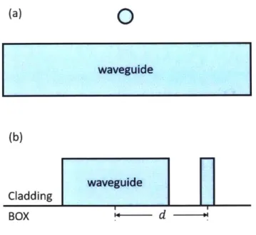
(a)
0
waveguide
(b)
waveguide
Cladding
BOX . dFigure 2-1: Demonstration of a silicon pillar defect in proximity to a straight silicon waveguide: (a) Top view; (b) Side view.
particle introduced during the photo-lithography process, the other is the ball-shaped particle introduced by foreign metal.
In the thesis, we always set the z-axis to be perpendicular to the circuit plan, and the location of the particle only depends on x and y while its z-position is fixed. For example, the pillar-shaped particle has the same height and same z-position as the silicon waveguide (Figure 2-1, Figure 2-2); the ball-shaped particle lies on the surface of the buried oxide (BOX) (Figure 2-3). The demonstrations and results in this thesis all are based on a silicon waveguide with width 500 nm and height 220 nm, though the methods can be applied to other geometries.
2.2
S-Parameters
Scattering parameters (S-parameters) are commonly used to describe the behaviour of a linear time-invariant network. Traditionally, this concept is used to describe the response of electrical devices, but they can be used to describe optical devices as well.
(a)
0
waveguide
(b)
I Iwaveguide,
Cladding
BOX
d
Figure 2-2: Demonstration of a silicon dioxide pillar (within) a straight silicon waveguide: (a) Top view; (b)
(a)
hole defect in proximity to Side view.
0t%
waveguide
(b)
waveguide
Cladding
BOXd
Figure 2-3: Demonstration of waveguide: (a) Top view; (b)a metal sphere defect in proximity to a straight silicon Side view.
For example, a two-optical-port device can be described as a matrix [2]:
b(
S1 1 S12 a1S
a, (2.1)b2 S21 S22 a2
J
a2)where a, describes the light incident on port 1, b, describes the reflected light at port
1, and b
2describes the transmitted light at port 2. The S-parameters are generally
complex, including an amplitude response and a phase response.
2.2.1
Mode Expansion
The S-parameters can be extracted from FDTD simulations, but a mode expansion
is necessary to separate the waveguide modes of interest from the simulation field.
Fortunately, in non-absorbing waveguides, the waveguide modes are power
orthogo--nal, which gives the mode expansion coefficients for an arbitrary electric field E and
magnetic field H, and modal fields Em and Hm, both on the surface &Q [21]:
a = 1
dS.ExH* +
dS.E*
xH,
(2.2)
b
dS.ExH* -
dS -E*x H ,
(2.3)
N
= -jdS
- Em x H*, (2.4)2 a
where a is the forward mode coefficient, b is the backward mode coefficient, and
N, corresponding to the power of the mode, is real for non-absorbing materials.
S-parameters can be calculated from an S-parameter matrix sweep simulation combined
with these mode expansion coefficients. For example, S
12can be evaluated by a
simulation where the source mode (see detail as in Section 2.2.2) is injected from port
1 and the monitor is at port 2:
= amonitor Nmonitor
S12- asourceVNsource (2.5)
and appropriate a or b coefficient will be used for
amonitorand
asourcedepending on
the direction of the mode.
It is straightforward to notice that N only depends on the port and does not change through different simulations. Similarly, since the source mode is injected from every port exactly once in an S-parameter sweep (e.g., S12, S13, ... are evaluated from the same simulation in which the source mode is injected from port 1), the corresponding
asource only depends on the port as well. Thus, we denote Ni, si as N coefficient, amonitor at port i and a2j, Ei as amonitor at port
j;
and electrical field from simulationwhere source mode is injected from port i, respectively in the rest of the thesis. Using this notation, (2.5) can be rewritten in general as
S = aiN N. (2.6)
2.2.2
Equivalent Source Theory
Another question around S-parameters simulations is how these source modes are generated. In Maxwell's equations, sources are represented in either dipole form (i.e., polarization P and magnetization M) or current form (i.e., electric current density J and magnetic current density K), which are connected through the continuity equation:
OP am
J -iwP, K = tto = -iwtpoM, (2.7)
at
at
where w = 27rf is the angular frequency. So the question is: what is the dipole source (P, M) or current source (J, K) that generates fields (Es = sEm, HS = sHmn) in
some region Q?
Equivalent source theory implies that for a source-free field (Es, HS) in region Q and no field outside , the corresponding current source is the surface current on &Q [22]:
Js
-(n x Hs) 6(DQ),
(2.8)
KS
=(n x Es) 6(OQ),
or equivalently in dipole form using (2.7), i
Ps
= - (n x Hs) 6(&Q),(2.9)
Ms = (n x Es) (aQ), W/10
where n is the normal unit vector of the surface OQ, and 6(OQ) is the Dirac delta distribution that equals zero everywhere except for the surface 9Q and has the in-tegral
f O(x)J(OQ) d x
=fQ
#(x)
dS for any continuous test function#(x).
Thisprovides reference and understanding of how the source mode is generated in FDTD simulations.
2.3
Adjoint Method
The adjoint method (or adjoint state method) is a numerical method for efficiently computing the gradient of a function in a numerical optimization problem or for sen-sitivity analysis [23]. It has several different forms in different fields of application, but one can find a general derivation from the form of differential-algebraic equations in [24]. Specifically, the matrix form used for linear system analysis is easy to demon-strate [25]. Suppose we want to find the derivative of the output y(p) of a linear system with variation parameters p:
A(p)x(p) b, y(p) = cTx(p). (2.10)
Then it is easy to find that
dy(p)
-c
T A(p)- 1dA(p)
(2.11)
dp
dp
Thus the derivative at certain point po can be computed using two system solves:
A(po)x(po)
=b
and A(po)Tv =c,
anddy
= _VTdA
x(pO), (2.12)dp
POdp
POwhich can be very efficient if the number of variation parameters is much greater than the number of outputs.
2.3.1
Adjoint Method in Electromagnetics
Maxwell's equations is an example of linear system analysis, where x(p) is electro-magnetic field (E(x), H(x)), A(p) is related to permittivity E(x), and b is the source dipole (P(x), M(x)) or source current (J(x), K(x)). The output (real-valued) merit function
F(E, H) =
x
f(E(x), H(x)) d'x (2.13)
is nonlinear in general, but can always be linearized around nominal point:
WF = 2Re
[f
(
=
Le
E(x)
-SE(x)
+ OH aH~x(x)
Thus c is (Of/OE(x), Of/OH(x)) in this form. We almost have a glimpse of the final formula for the adjoint method in electromagnetics by this analysis; indeed, it is possible to obtain the formula from (2.12). But here we take a different approach that gives us more physical insight into the problem, which was first proposed and implemented for optimization in [15].
Firstly, the effect of an infinitesimal perturbation of permittivity e(x') in region 7P is equivalent to introducing a dipole source
Pind(X) )E(x') (2.15)
in the same region, for a first-order approximation. Thus the perturbation (6E(x), 6H(x)) from P(x') is
6E(x)
=j G xEP XI) pind (x') d3x' =6H(x)
= GHP(X; XI) pind (x') d'x' =I
G EP (x; x')6E(x)E(x') d3XI,10GHP (X; x') 6E(x') E(x') d 3X
(2.16)
Notice that plugging (2.16) into (2.14) produces terms that look like Pi(x) -GEP(X; X')P2(x') and M1(x) -GP(x; X')P2(x'), thus we can swap the order of the
inner product using reciprocity of Maxwell's equations:
Pi(x)
-
GEPx;X)P2(x') = P2(x') - GEP(x; x)Pi(x),poMi(x)
-GHP(x; X)P 2(x') = -P 2(x') -GEM(x; x)MI(x).Taking (2.16) and (2.17) into (2.14) and properly rearranging the order of integral, we get
F = 2 Re
j6(x')E(x')
-EA (x') d'x' (2.18) whereEA(xI) = GEP (x'; x)
(x)
-GE(X;
X) a(X) d3x (2.19)is the eletric field from adjoint simulation for the same structure with dipole sources (P, M) = (af/&E, -(1/to)Of/&H) in the region x. Since the adjoint field EA only depends on the merit function but not the variation of permittivity, one single ad-joint simulation is enough to compute any possible infinitesimal permittivity varia-tion. Moreover, the adjoint simulation is based on the original struture without any perturbation, thus it does not require a fine mesh grid for high accuracy, as the direct method does.
Chapter 3
Adjoint Method on Particle
Defects
In this chapter, we discuss how to apply the adjoint method on the particle defect problem. In particular, we focus on the impact of small particle defects on the S-parameters of photonic device components. To begin, we adapt the adjoint method for S-parameters in Section 3.1. Next, we discuss why particle defect is a special type of permittivity perturbation and needs special care in Section 3.2. Section 3.3 discusses and summarizes the effectiveness of the method that we develop.
3.1
Adjoint Method for S-Parameters
Although an implementation of the adjoint method wrapped around Lumerical FDTD has been proposed in [15], the figure of merit (FoM) was presumed to be real (for the purpose of optimization design), while the S-parameters we are modeling are complex. Despite the fact that it is feasible to model the amplitude response and the phase response separately, a more concise solution is to derive the adjoint method in the same path as [15] for S-parameters exclusively.
Since any S-parameter is proportional to either a in (2.3) or b in (2.4), here we demonstrate the adjoint method applied on the a coefficient, and the same results can be easily derived for b and thus S. In general, a complex merit function F(E, H) has much more complicated forms of derivatives form than that in (2.14). However,
for a holomorphic function f(E, H) where af/&E* = af/&H* = 0, the result is straightforward as
F
j
(x)- SE(x) +
a(x)
-
JH(x) d x. (3.1)fXI E aHI
The differences between (2.14) and (3.1) are just the factor of 2 and the real part operator. Thus the result from the adjoint method is similar as well,
5F
j
6E(x')E(x') -EA(x') d
3x',(3.2)
with the same adjoint field as in (2.19).
Fortunately this is the case for the a coefficient, thus it is easy to obtain the adjoint dipole sources:
1
P(x) =(n
xH* ) 6(aQ),
4N
(3.3)
M(x) = - 1 (n x E* )(aQ).
Compared with (2.9), this is actually the equivalent current sources of the mode source
iW iW
HS =mH*, 4N m4N ES= E*, (3.4)
which is exactly the backward-propagating mode with amplitude iW/4N.
It is unnecessary to specify the amplitude of the mode source in FDTD simulation; instead, the mode source is generated with an arbitrary amplitude s, which later can be obtained from the mode expansion monitor. In such scenario, we can write the variation in a as
6a
=
4sN
f
E(x')E(x') -EA (x') d
3x',(3.5)
where the adjoint field EA comes from a backward mode with amplitude s.
Now we try to expand the case for S-parameters. If (3.5) is used in the calculation of aij for Sij, then the forward field E is Ei from simulation for Sij, and the adjoint field EA is Ej from simulation for Sji. This suggests that the adjoint simulation of one S-parameter simulation is just the reciprocal S-parameter simulation. Therefore,
an S-parameter matrix sweep is able to cover all of the S-parameter simulations with their adjoint simulation, and no additional simulation is needed for adjoint analysis. From (2.6), we have
si =
f
As ss V N_Nj IV
k
(x') E (x') -
Ej (x') d3x', (3.6) or written in the form of transmission T = IS12 and phase#
= arg(S),w a*.f 6T= -
IN
j3J 21si 12Nj sj 6E(x')E (x') -
Ej (x') d 3x', (3.7)(3.8)
_ i16o4i = WRe 1 36(x')Ej(x')- E(x') d3x'.
4Nj asjs V)
3.2
Polarizability
While it may not be intuitive, the dipole approximation in (2.15) does not hold for finite permittivity variation. The reason is the discontinuous interface introduced by particle.
We consider a simple example first: a dielectric sphere (permittivity E1) in vacuum
&o with uniform electric field E. While the relationship (2.15) still holds for overall total field:
pind = (El - Eo)Etot,
(3.9)
the polarization charge on the surface of sphere will induce an extra electric field inside the sphere and thus change the total field:
(3.10)
Combining (3.9) and (3.10), we have
(3.11)
When Ei -+ 6o, -y = 30/(61 + 2eo) reaches 1, and thus (3.11) goes back to (2.15). In general, pind can be not parallel to E, and can even be non-uniform. But for the case where the particle is small, what matters most is not the polarization pind but
pind
Etot
=E
- .nd
3EO
Pind = 3Eo
-(1
-co)E
='yZE.
the dipole moment
pind =J Pid(x') d3x'. (3.12) The relationship between the dipole moment of a particle and the electric field is known as: [26]
p ind = aE,
(3.13)
where the polarizability a, inspired by (3.11), can be expressed as
a = yVAE,
where V is the volume of the particle, the factor -y can be scalar or tensor, depends on the shape of the particle, as well as the permittivity of the particle its environment E, but it always symmetric and satisfies
lim Y = 1. AE-+0 (3.14) and -y E and
(3.15)
We list a few analytic examples of -y as a function of EP, e for different shapes in Table 3.1. In general, we always have -y < 1 when E, > E, and y > 1 when E, < E. This means that a silicon particle in the oxide cladding is less significant than an oxide hole of same volume in the silicon waveguide, even under the same amplitude of electric field - we will see validated examples in the next chapter.
Table 3.1: Analytic examples of -y as a function of eP, E for different shapes.
Shape Sphere Cylinder Cylinder
(tall approximation) (flat approximation)
32
EP2e (2e/(E+
E)
2E/(Ep+)
1 1e
+ 2E ) EI1
Under the small particle approximation, (3.2) can be written for a particle intro-duced at xp:
and when the FoM is S-parameters,
Asi= 4
NNExN)-
Es(x). (3.17)4As isj VNiNj
3.3
Limitations
Before we jump into the implementation of the adjoint method on different photonic devices, we want to make a summary of all the approximations in the method we have made so far, and their possible implications in terms of potential errors in real-life implementations. This will serve as explanation for part of the validation result in next chapter.
The dipole approximation used in (2.15) and (3.13) is a commonly used first-order approximation in electromagnetics, which ignores higher order effects, e.g., magnetic dipole, quadrupole, etc. Such higher order effects can be significant for large pertur-bation - this is less important in the particle defect problem since large-sized particle rarely occurs. But they can also be significant when the first order effect is zero, which means that if AF calculated from the adjoint method is 0, the real variation
AF is likely to be non-zero (although it is small in most cases) because of the higher
order effects.
Specifically for particle defects, the approximation used in (3.13) and (3.16) also assumes that the electric field around the particle is uniform, which suggests that the size of particle should be much smaller than the length scale of change of the electric field. However, some particle defects do not satisfy such criteria, e.g., the silicon pillar defect from photo-lithography has same height as the waveguide, which is comparable to the length scale of change of the electric field in that direction. It is also hard to determine an exact location (xp in (3.16)) for the particle in such case, so we will try to average the field over the region within the particle Op:
-yE(xp) -E^(xp)
~
J
-yE(x) -
EA (x) d
3x.
(3.18)
The averaging approach potentially introduces higher order error, but it could be small when the field is varying slowly. Such assumption can be even more problematic
for metal particles, since the field tends to gather near the surface of conductive material at high frequency, which is known as the skin effect. Thus the size of particle needs to be even smaller for proper dipole approximation. Even when these criteria are satisfied, the factor -y usually has some deviation from its theoretical value.
When the particle defect intersects with the material interface (e.g., the waveguide sidewall in most cases), either the actual shape of the particle changes, which makes it difficult to evaluate the shape-dependent factor -/, or the electric field is discontin-uous, which breaks the uniformity assumption. We simply neglect these transition areas in our application, as they are extremely small for small particles, and we can approximate the behavior through interpolation if needed.
In general, a nonlinear merit function can introduce extra error in the linearization process in (2.14) or (3.1); but S-parameters happen to be linear functions, adn are thus free from these potential error. In the next chapter, we consider examples where the change in S-parameters is large compared to its original value, but the adjoint method still gives accurate enough results. However, since the transmission and phase are non-linear functions of S-parameters, the adjoint method in these forms introduces extra error and can be inaccurate when the nominal Sij is close to zero.
Chapter 4
Implementation on Photonic
Device Components
In this chapter, we will show the implementation of the adjoint method developed in Chapter 3 on several different photonic device components: a straight waveguide in Section 4.1, a y-splitter in Section 4.2, and a directional coupler in Section 4.3. We will explain the simulation setup in each section, and validate the adjoint method by comparing to results from direct simulation. For complicated components like the y-splitter and directional coupler, a point-to-point validation is infeasible, so we will only consider a number of signature locations for direct simulation. The operation wavelength is 1550 nm for these examples; some figures show results for a spectrum ranging from 1500 to 1600 nm; we will discuss these additional wavelengths in Chapter 5.
4.1
Straight Waveguide
We set the straight waveguide to propagate light along the x axis, and put port 1 at x = 0 and port 2 at x = L. From the propagating theory, S12 = exp (inekL) and
where ne is the effective index of the waveguide mode, and k = 27r/A is the angular wavenumber in vacuum. Using (3.17), we have
iwVAe
AS, = 4 yEm(y, zp) Em(yp, z)e2
inkxp, (4.2)
4N
iwVAE
AS12 = 4 7Em(yp, zp) E*((y), z)einekL
We define transmission T = T12, reflection R = T11, and phase shift
#
=#12;
then AT = Im A-yEm(yp, zp) - E*(yp, zp), (4.4) 2NwV
A0 = Re AyEm(yp, zp) - E* (yp, zp), (4.5)4N
w
2y
2AR = 16N2 jAeyEm(yp, zp) -Em(yp,
z,)I
2.
(4.6)Before making any assumption about the type of particle defect, there are several things we can observe from these expressions. Firstly, x, does not appear in any of these variations. Since z, is a fixed number for a certain type of particle with certain size, it suggests that there is only one degree of freedom in this problem, which is the distance d from the center of the particle to the center line of the waveguide (as shown in Figure 2-1, Figure 2-2, and Figure 2-3). This is consistent with our intuition. Secondly, AR
oc
V21AI2 is a second order effect that is always very small compared to AT and A0. Moreover, all we need from the simulation is the mode profile Emand its power N, which can be obtained from an eigenmode solver rather than FDTD simulator. Finally, for the fundamental TE mode of a silicon waveguide specifically,
Emz is small and negligible, and EmE*y is always a pure imaginary number1 , thus
-yEm(yp, zp) - E* (yp, zp) =
YxxEmx(yp,
zP)12+ _yyyEmy (yp, z)12
.
(4.7)
Therefore, only two diagonal elements of the tensor -y contribute to the variation in transmission and phase shift.2
'These statements are not necessarily true for complicated devices. In the Lumerical MODE and FDTD solver, Emy and Emz is always set to be real-valued, and thus Emy is pure imaginary.
2
4.1.1
Silicon Pillar and Silicon Dioxide Hole
For a non-absorbing particle, AR can be too small to detect in simulation; thus, here we mainly focus on the transmission and phase shift induced by the defect. Since AE and -y are real for non-absorbing materials, and also using (4.7),
AT = 0, (4.8)
wVAe
A# = 4N
(yxx
Emx(yp, z) I2 + -yyyIEmy (yp, zp) 2 (4.9)For a cylinder-shaped pillar, -yx = yyy = y,3 thus
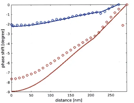
A - wVyA IEm(yp, z,) 1, (4.10)
4N
where -y = 2Eclad/(Eclad + Esi) = 0.3 for a silicon cylinder pillar in oxide cladding, and y = 2esi/(eclad + Esi) = 1.7 for an oxide cylinder hole in the silicon waveguide. (4.8) does not mean there is no transmission loss in a straight waveguide, but its first order effect is zero. On the other hand, from conservation of energy, we must have AT + AR < 0, which gives AT < 0. Therefore, it would be more appropriate if we
write it as
AT = O(IVAE12). (4.11)
As mentioned in Section 3.3, the height of the pillar h = 220 nm is too large to determine the value of z,, thus we average over the z-axis:
A WVyAE h Em(yp, z)12 dz. (4.12)
4Nh 0
We test the adjoint method on both a small particle (r = 20 nm) and a large particle (r = 40 nm). For the oxide hole, the phase shift predicted by adjoint method shows good consistency with direct simulation (Figure 4-1), and even for the large particle, the error is still in a reasonable range. On the other hand, the same method does not work so well for the silicon pillar (Figure 4-2) since the electric field is varying too much near the interface, which happens to be the position with maximum impact. 3A cylinder is not the only shape that satisfies this requirement; a square pillar, an octagon pillar, etc. also have -y, = yy = -y, although the value of -y is different.
0
20
-4
0 50 100 150 200 250
distance [nm]
Figure 4-1: The impact of a silicon dioxide hole pillar defect of
r
=20 nm (blue) and
r
=40 nm (red) on phase shift of a straight waveguide, as a function of distance d,
evaluated from direct simulation (circle) and adjoint method (solid line).
However, since the impact of the silicon pillar defect is much smaller than the impact
of the dioxide hole of the same size, the absolute error from the adjoint method for
the silicon pillar defect is still acceptable.
We also show the transmission impact from direct simulation in Figure 4-3 and
Figure 4-4. These are the higher order effects that are ignored in the adjoint method,
and here we see they are indeed negligible.
4.1.2
Metal Sphere
For a sphere-shaped particle, -y is a scalar. Thus
wV
AT = E(y, z) 2
Im yde,
(4.13)
2N
wV
A#=
Em(Yp,
z,)|
2Re yde,
(4.14)
4Nw2 V2
7 9 6 00 5 - 4-3 2 - --220 240 260 280 distance [nm] 300 320 340
Figure 4-2: The impact of a silicon pillar defect of
r =
20 nm (blue) and
r =
40 nm
(red) on phase shift of a straight waveguide, as a function of distance d, evaluated
from direct simulation (circle) and adjoint method (solid line).
100 150
distance [nm]
)
200 250
Figure 4-3: The impact of a silicon dioxide hole pillar defect of
r =
20 nm (blue) and
r =
40 nm (red) on transmission of a straight waveguide, as a function of distance d,
evaluated from direct simulation.
1 0.9 0.8 F P-9 0. 0. C 0. M 0. C 0. 0. 0. 0 0 0. I b0
1
0.9981 0.996 0.994 0.992 0.99 1 0.988 0.986 0.984 0.982 00 0 00 0 000 0 0 0 0 0 0 0 0 0 ooeooo O 0 -0 0.98 0 500.9996 0.9994 00 -C 0.9992 -0.999 0.0 c 0.9988 -0 0.9986
E0
L 0.9984 0.9982 -0.998 0.9978 ' 220 240 260 280 300 320 340 distance [nm]Figure 4-4: The impact of a silicon pillar defect of
r
=20 nm (blue) and
r
=40 nm
(red) on transmission of a straight waveguide, as a function of distance d, evaluated
from direct simulation.
where -y = 3c/(cp + 2c). We test four different metal materials that are commonly
used in integrated circuit fabrication: Aluminium, Copper, Tungsten, and Titanium.
As with the pillar defect, we test both small particle (r = 20 nm) and large particle
(r = 40 nm) cases.
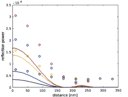
We begin our analysis with the small particle. The adjoint method captures the
impact on phase shift (Figure 4-7) relatively well, but for highly conductive materials like Aluminium and Copper, it seems to underestimate the transmission impact (Fig-ure 4-5). This can be understood as error in the polarization factor -y; thus we can try to make a correction to match the result from direct simulation. For the impact
on back reflection (Figure 4-9), the adjoint method and direct simulation show
sim-ilar trends but different values; however, we cannot guarantee the accuracy of direct simulation since the value is too small.
However, the adjoint method does not produce reasonable results for the large particle case. There is a trend in direct simulation that obviously cannot be matched
by simple correction on -y, e.g., the impact of Tungsten defect on phase shift (Figure 4-8). And comparing with the results for the small particle, we see many values that
0 50 100 150 200 distance [nm]
250 300 350
Figure 4-5: The impact of a metal sphere defect of
r =
20 nm on transmission of a
straight waveguide, as a function of distance d, evaluated from direct simulation
(cir-cle) and adjoint method (solid line). Four different materials are tested: Aluminum
(blue), Copper (red), Tungsten (yellow), and Titanium (purple).
0 50 100 150 200
distance [nm]
250 300 350
Figure 4-6: The impact of a metal sphere defect of
r =
40 nm on transmission of a
straight waveguide, as a function of distance d, evaluated from direct simulation
(cir-cle) and adjoint method (solid line). Four different materials are tested: Aluminum
(blue), Copper (red), Tungsten (yellow), and Titanium (purple).
1
0.995 0.99 6. 0 .1Zo
0 0 " 0o
oX 0 0 'A A' 7' 0o
-0.985 0.98 0.9751
0.95 6-C 0. 0 E in QU 00 0 0 0 , 0 0 0.9 0.85 0.8 0.750 50 100 150 200 distance [nm]
250 300 350
Figure 4-7: The impact of a metal sphere defect of
r =
20 nm on phase shift of a
straight waveguide, as a function of distance d, evaluated from direct simulation
(cir-cle) and adjoint method (solid line). Four different materials are tested: Aluminum
(blue), Copper (red), Tungsten (yellow), and Titanium (purple).
9 8 7 6. M a 4 a.' 2 1 0 0 50 100 150 200 distance [nm] 250 300 350
Figure 4-8: The impact of a metal sphere defect of
r =
40 nm on phase shift of a
straight waveguide, as a function of distance d, evaluated from direct simulation
(cir-cle) and adjoint method (solid line). Four different materials are tested: Aluminum
(blue), Copper (red), Tungsten (yellow), and Titanium (purple).
0.8 0.7 0.6 P" a.' U' 0 0 - 0o
-0 0 0.3 0.2 0.1 F3.5 3 2.5 2 0 f1.5 1 0.5 0 0 50 100 150 200 distance [nm] 250 300 350
Figure 4-9: The impact of a metal sphere defect of
r =
20 nm on back reflection of a
straight waveguide, as a function of distance d, evaluated from direct simulation
(cir-cle) and adjoint method (solid line). Four different materials are tested: Aluminum
(blue), Copper (red), Tungsten (yellow), and Titanium (purple).
0.03 0.025[ L_ 0.02 o 0.015 w0 0. 0.005 0' 0 50 100 150 200 distance [nm] - 30 91 0 250 300 350
Figure 4-10: The impact of a metal sphere defect of
r =
40 nm on back reflection of a
straight waveguide, as a function of distance d, evaluated from direct simulation
(cir-cle) and adjoint method (solid line). Four different materials are tested: Aluminum
(blue), Copper (red), Tungsten (yellow), and Titanium (purple).
0 0 0
0
0 00 0 00N.
~8
o
8
0 0S
0 0 0 0 0 0break the law of the adjoint method where the impact is always proportional to the volume of the particle.
So far we see that for small particles, silicon dioxide hole pillar defects have the most impact on a straight waveguide, which happens to be the most accurate to predict from the adjoint method. For large particles, metal sphere defects can have stronger impact, but out of the appropriate range of the adjoint method. In the following sections and chapters, we thus only show examples of silicon dioxide hole pillar defects with r = 20 nm; the same methodology can be used for other types of defects, but we expect it to have either weaker impact (for small particles) or lower accuracy (for large particles).
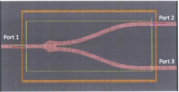
4.2
Y-Splitter
In this section, we choose to model the impact of particle defects on the power-optimized Y-splitter in [27]. We label the input port as port 1, and the output ports as port 2 and 3. Based on the symmetry of the nominal design, we have
E3x(x, y, z) = -E2x(x, - y, z)
E3y (x, y, z) = E2y (x, -y,z) (4.16)
E3z(x, y,z) = -E2z(x, -y, z)
and S13 = S12, S33 = S22. Therefore, a complete S-parameter sweep need only include simulation from port 1 and port 2, and the results for port 3 can be obtained by flipping the field of port 2. However, the particle defect analysis cannot skip port 3, as the introduced particle breaks the symmetry.
We will do a complete S-parameter analysis, but in this section we only focus on a few of them: the upper branch transmission T12, phase shift
#12,
and itsself-reflection R2 = T22. The setup in FDTD is just the normal S-parameter sweep setup
plus the field monitor (Figure 4-11); the port elements are used for both S-parameter calculation and necessary mode expansion coefficients for the adjoint method. In order to reduce memory cost, the field monitor is set to record only electric field and only at the wavelength of interest A = 1550 nm.
Figure 4-11: The implementation of the adjoint method on y-splitter in Lumerical FDTD simulation. The yellow box in the middle is the added field monitor. If the output of interests are only T12, 412 and R2, the port element at port 3 is optional,
while it is still required in complete S-parameters analysis.
We show the impact of a silicon dioxide hole pillar defect of r = 20 nm in Figure 4-12, Figure 4-14, and Figure 4-16. As we would expect, the particle in the upper branch contributes mostly to A# 12 and less to AT12, which is similar to the case of straight waveguide. The particle in the cavity introduces asymmetry and thus impacts transmission distribution. Finally, the lower branch has little contribution to all three outputs of interest in the upper branch.
We choose the point at the cavity taper where the adjoint analysis shows max-imum transmission impact in Figure 4-12 to do a direct simulation validation. We intentionally show the zero-impact axis in the comparison plot (Figure 4-13, Fig-ure 4-15, and FigFig-ure 4-17) to get a better sense of relative error. Overall, the adjoint method shows excellent consistency with direct simulation; even for the back reflec-tion of upper branch, where the impact has the same magnitude as the nominal value, the prediction from the adjoint method is still highly accurate.
4.3
Directional Coupler
We next consider a directional coupler (Figure 4-18) with coupling length L, = 4.5 Pm and gap width w9= 200 nm which we will use to build a ring resonator in Chapter 6.
-0.015 -0.01 -0.005 0 0.005 0.01 0.015
Figure 4-12: The mapping of the impact of a silicon dioxide hole pillar defect of
r =
20 nm on the upper branch transmission T12
of the y-splitter structure, as a
function of the spatial location of the defect. Zoom-in around the cavity.
0
-0.002 -0.004 <--0.006 --0.008 --0.01 --0.012 -0.014 -0.016 1500 1520 1540 1560 wavelenth [nm] 1580 1600Figure 4-13: The impact of a silicon dioxide hole pillar defect of
r =
20 nm at selected
location on the upper branch transmission T12
of the y-splitter structure, evaluated
from adjoint method (blue) and direct simulation (red).
-0.005 0.01 0.015 -0.015 -0.01 -0.005 0
-0.04 -0.03 -0.02 -0.01 0
l,12
0.01 0.02 0.03 0.04