by
Masood Qazi
Bachelor of Science in Electrical Science and Engineering Bachelor of Science in Physics
Massachusetts Institute of Technology (2006)
Submitted to the Department of Electrical Engineering and Computer Science in Partial Fulfillment of the Requirements for the Degree of
Master of Engineering in Electrical Engineering and Computer Science at the
MASSACHUSETTS INSTITUTE OF TECHNOLOGY February 2007
c
°2007 Massachusetts Institute of Technology. All rights reserved.
Author:
Department of Electrical Engineering and Computer Science February 2, 2007
Certified by:
John K. DeBrosse Senior Technical Staff Member, IBM Thesis Supervisor
Certified by:
Anantha P. Chandrakasan Professor of Electrical Engineering Thesis Supervisor
Accepted by:
Arthur C. Smith Professor of Electrical Engineering Chairman, Department Committee on Graduate Theses
by
Masood Qazi
Submitted to the Department of Electrical Engineering and Computer Science on February 2, 2007, in Partial Fulfillment of the Requirements for the Degree of
Master of Engineering in Electrical Engineering and Computer Science
Abstract
The circuits for a A 4kb array of Magnetic Tunnel Junctions (MTJs) have been designed and fabricated in a 0.18µm CMOS process with three levels of metal. Support circuitry for addressing, reading, writing, and test mode probing enables the characterization of the switching of a thin-film ferromagnetic layer in the MTJs. Specifically, novel mechanisms involving spin-transfer or thermal assistance can be studied and compared to current MRAM designs that switch the MTJ with current-induced magnetic fields. Using this array design, both high speed digital and quasi-static dI/dV experiments can be conducted to investigate the nature of the MTJ resistance hysteresis and process variation in addition to the switching behavior under both polarities of current.
Thesis Supervisor: John K. DeBrosse Title: Senior Technical Staff Member, IBM
Thesis Supervisor: Anantha P. Chandrakasan Title: Professor of Electrical Engineering
At the heart of the semiconductor industry is semiconductor memories, and at the heart of semiconductor memories is IBM. The kind of project I have had the fortune to undertake could only have come to fruition under the auspices of IBM memory development.
First, I would like to thank Andy Anderson for taking the risk to hire me in 2004. I am also grateful to my manager John Gabric for compelling me to meet his high expectations and return every year since my first assignment. I suspect that only later in my professional career will I fully appreciate how lucky I was to have him as my first “boss.” I also appreciate the support from Bill Gallagher at IBM research for his role in conceiving a challenging, risky project for me and providing the guidance at critical junctures of this work that made it succeed as a thesis.
The MRAM processing technology involved in this project is based on the comprehen-sive body of knowledge and expertise cultivated by the MRAM team at IBM research. In particular, Solomon Assefa has played a central role in developing the process for fabricating the experimental magnetic tunnel junctions for which this 4kb array was intended. Further-more, Jonathan Sun has been forthcoming in discussing his research on spin transfer effects in nanomagnets in addition to introducing me to the rich field of magnetism and magnetic materials. Janusz Nowak has also helped in characterization measurements on magnetic tunnel junctions that have guided my experiments.
For the circuit design, which is more immediate to the contributions of this thesis, I would like to thank Tom Maffitt for sharing his insight obtained over years of experience in DRAM and, more recently, MRAM design. I also appreciate Mark Jacunski’s willingness and ability to teach me about memory circuit design, particularly for his methodical approach to inte-grated circuits and for taking time from his demanding responsibilities in embedded DRAM design. I would also like to thank Mark Lamorey for his extensive work on mask-related processing issues; he ultimately ensured that my design data got appropriately translated to physical masks for fabrication.
I am grateful to Mark Wood for not only his assistance in the layout of this project but for taking me through the elements of laying out a complex chip design with 106 to 109
transistors, drawing upon principles of hierarchy, robust wiring, techniques for tight pitch circuits, and device matching for analog circuits. His personality made the weeks of sitting with him in front of the layout software tools much more enjoyable than they should have been. This project also received significant contributions from Kim Maloney in laying out several circuit blocks of the 4kb Array.
For the formidable task of wafer-level test on a memory array with over 40 signals— several of which require timing control on a time scale of 10ns—I cannot emphasize enough the vital role of John Parenteau and the memory tester which he helped develop over the course of twenty years. His test environment enabled me to exercise the array in several different ways, many of which were unanticipated during the design phase. In fact, the memory tester functioned as almost an extension of the integrated hardware on the wafer— in my incremental approach to extracting functionality from experimental, uncontrolled,
helping me with testing. His problem solving skills and fearless attitude in the face of new and unexpected challenges with electrical equipment helped me overcome severe obstacles to the data gathering phase of this project.
Finally, my mentor John DeBrosse has been involved in each step of this project, keeping me on a path—for over one and a half years—that ultimately resulted in viable integrated hardware. In working with him, I have experienced a form of teamwork beyond the mere partitioning of responsibilities; his feedback and ideas shaped my inchoate thoughts into a design for a 4kb memory array and exposed me to work in MRAM and DRAM beyond the scope of my project. Because of his experience in the multifaceted elements of memory development and ability to articulate his thought process, he has made work in MRAM circuit design challenging, exciting, and rewarding. In the course of my career, I hope to acquire such elements of technical leadership.
It is self-evident from the nature of the work described in this thesis how dependent it was upon these people. Remarkably, they made their contributions to my thesis in parallel to fulfilling their own work obligations. May this project ultimately reflect an additional capacity of theirs to advance memory technologies.
Masood Qazi Cambridge, MA
1 Introduction 13
1.1 The Memory Landscape . . . 14
1.2 Previous MRAM Work . . . 16
1.3 Problem Statement . . . 18
1.4 Contributions of this Work . . . 19
2 Magnetics Review 21 2.1 The Magnetic Dipole . . . 21
2.2 Properties of Nanomagnets . . . 32
2.2.1 The Fields and Energy of a Nanomagnet . . . 33
2.3 Magnetization Dynamics . . . 40
2.4 The MTJ structure . . . 41
2.5 Spin Angular Momentum Transfer . . . 42
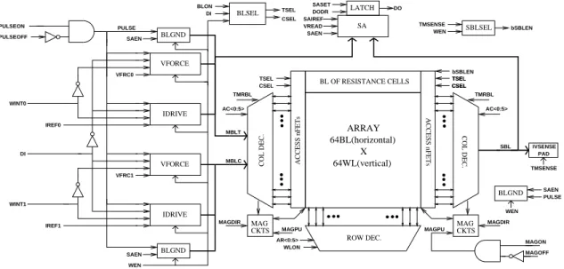
3 Design of the 4kb Array 47 3.1 Overview . . . 47 3.2 The Cell . . . 49 3.3 Row Path . . . 54 3.4 Column Path . . . 56 3.4.1 Control Logic . . . 56 3.4.2 MBL/SBL grounding . . . 57 3.5 Magnet Wire . . . 59 3.6 Sense-amplifier . . . 62
3.6.1 Sizing of mirrors and source follower clamp device . . . 65
3.6.2 Design of transconductance amplifier . . . 67
3.6.3 Analysis of loop dynamics . . . 78
3.6.4 Transient operation . . . 81 3.7 Write Drivers . . . 82 3.8 Operation . . . 83 3.8.1 PULSE timing . . . 84 3.8.2 Standard Write . . . 84 3.8.3 Standard Read . . . 86
3.8.5 TMSENSE . . . 88
3.9 Layout Floorplan . . . 88
4 Testing 89 4.1 Test Setup . . . 91
4.2 Experimental Results on Resistance Bitline . . . 94
4.2.1 Write Pulses . . . 94
4.2.2 Read Pulses . . . 97
4.2.3 Senseamp Reference Sweep . . . 106
4.3 Description of Initial Test Plan . . . 111
4.4 Results from Field Switching . . . 115
5 Conclusion 119 5.1 Summary of Contributions . . . 119
5.2 Future Work . . . 120
A Electromagnetics Reference 121 A.1 Maxwell’s Equations . . . 121 A.2 Derivation of Spin-Transfer Switching Dynamics for a Mono-domain model . 122
1.1 The memory landscape . . . 16
2.1 The dipole field . . . 22
2.2 Calculation of magnetic field . . . 22
2.3 A current loop . . . 24
2.4 Classical precession . . . 27
2.5 Magnetized ellipsoid along the “easy” axis . . . 34
2.6 Magnetized ellipsoid along the “hard” axis . . . 34
2.7 The Stoner-Wolfarth Astroid for a monodomain magnet . . . 39
2.8 The MTJ stack . . . 41
2.9 Representation of spin torque due to current between two ferromagnets . . . 42
3.1 Top-level block diagram of the ADM . . . 48
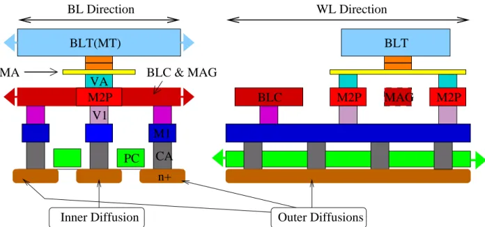
3.2 Schematic cross-section of array . . . 49
3.3 Spin-transfer switching in MTJs . . . 50
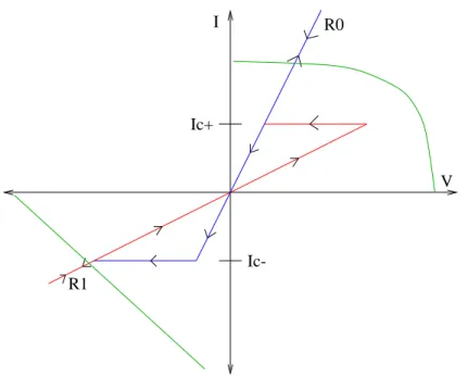
3.4 Loadline of IV hyteresis in a bidirectional cell . . . 50
3.5 Vertical cross-section of the memory cell . . . 52
3.6 Cell layout . . . 53
3.7 Schematic of a “one out of eight” predecoder.” . . . 55
3.8 Field produced by magnet wire . . . 60
3.9 Plot of field produced by magnet wire . . . 60
3.10 Circuits for one of three magnet wires . . . 61
3.11 Prior sense-amplifier topology. . . 63
3.12 Sense-amplifier topology. . . 65
3.13 Sizing of current mirror load . . . 67
3.14 Schematic of transconductance amplifier . . . 68
3.15 Full small-signal schematic of transconductance amplifier . . . 69
3.16 Simplified small-signal schematic of transconductance amplifier . . . 75
3.17 Feedback loop for M5 . . . 75
3.18 Small-signal schematic to calculate overal Gm . . . 76
3.19 Simulation of VTC of feedback amplifier . . . 77
3.20 Small signal circuit for stability analysis . . . 79
3.23 The outpout of the SA goes through two latches . . . 82
3.24 Schematic of current driver . . . 83
3.25 Timings for PULSE signal . . . 84
3.26 Timing diagram for write cycle . . . 85
3.27 Timing diagram for read cycle . . . 86
3.28 ADM floor plan for major core circuits . . . 88
4.1 MACE Block Diagram . . . 93
4.2 Current write pulses at Vdd = 1.8V . . . 95
4.3 Voltage write pulses at Vdd= 1.8V . . . 95
4.4 Current write pulses at Vdd = 3.6V . . . 96
4.5 Voltage write pulses at Vdd= 3.6V . . . 96
4.6 50mV read pulses with high resolution scope probe. . . . 98
4.7 Close examination of a 50mV read pulses for resistance value in the middle of the expected operating range. . . 99
4.8 50mV read pulses with high bandwidth scope probe. . . 100
4.9 Close examination of a 50mV read pulses for resistance value in the middle of the expected operating range (high bandwidth scope). . . 101
4.10 100mV read pulses with high resolution scope probe. . . 102
4.11 Close examination of a 100mV read pulses for resistance value in the middle of the expected operating range. . . 103
4.12 100mV read pulses with high bandwidth scope probe. . . 104
4.13 Close examination of a 100mV read pulses for resistance value in the middle of the expected operating range (high bandwidth scope). . . 105
4.14 The digital output correctly reads the resistance of the memory cell. . . 106
4.15 Read 0 failcount plot for a single cell. . . 108
4.16 Read 0 failcount plot for full array. . . 108
4.17 Successful extraction of resistance distribution on RBL. . . 110
4.18 Single cell failcount curves for both W1R0 and W0R0 test patterns. . . 114
4.19 Full array failcount curves for both W1R0 and W0R0 test patterns. . . 114
4.20 Cumulative distribution after W1 and W0 . . . 115
4.21 Histograms after W1 and W0 . . . 116
3.1 Small signal design considerations. . . 74
3.2 Functional description of normal operation . . . 84
3.3 Timing values for a write cycle. . . 85
Introduction
The three most significant semiconductor memories in today’s integrated circuit market are DRAM, SRAM, and FLASH. Each type of memory has a distinct set of advantages in terms of speed, density, non-volatility, and power. SRAM offers the fastest speeds but compromises on density because of a six-transistor (or sometimes four-transistor) cell. DRAM offers higher density with a one-transistor cell and storage capacitor but operates at slower speeds than SRAM. FLASH offers the density of DRAM and non-volatility but has write cycles several orders of magnitude slower than the other two RAM memories. Across these three memories, power is also a consideration through transistor off current in SRAM, refresh requirements in DRAM, and large write voltages and currents in FLASH [1].
Electronic systems like personal computers, mainframes, and mobile phones benefit from the distinct advantages of each type of memory. Thus, a need exists to more effectively integrate the different types of memories into one unit. A non-volatile RAM memory could be a “game-changer” to the semiconductor memory industry by offering the advantages of multiple memories in one chip [2]. For portable systems, it would allow for increased space and energy efficiency. In general, it would simplify system architecture, reduce hardware cost, and enable instant-on functionality. One possible candidate for non-volatile RAM is magnetoresistive random access memory (MRAM), which is comprised of arrays of Magnetic Tunnel Junctions (MTJs) whose states are stored as high or low resistances, depending on
the parallel or anti-parallel alignment of two thin-film ferromagnetic layers. Some of the advantages of MRAM as a “universal memory” are: it can retain its state with zero power; it is radiation immune in space applications; it requires 400 times less write power than FLASH; it has unlimited write endurance; and, it has comparable densities and speeds to SRAM and DRAM. [3].
Conventional MRAM memories have manipulated ferromagnetic layers in MTJs through current-induced magnetic fields, posing problems for isolating bits and working within the operating range of CMOS technology. This project aims to make a first step towards the development of a new kind of MRAM memory, differing from its predecessors through novel switching mechanisms based on spin-transfer or thermal effects. The vehicle for this investi-gation will be a 4kb array development macro (ADM) designed as a functional memory unit that also allows detailed experimental modes to measure the switching and read character-istics of MTJs.
1.1
The Memory Landscape
Shown in Fig. 1.1 is a comparison of the cost-performance tradeoff made by several types of memories. On the horizontal axis is the random access time. 1 This value corresponds to
the minimum time required between (1) a read or write operation at a given address in the memory and (2) a subsequent read or write operation at another, arbitrarily chosen, address location in the memory. For the vertical axis, the high-volume unit cost was divided by the memory size to give a cost per bit. One can also interpret this as a proxy for cell area, but the quotation in terms of $ permits comparison accross memory technologies that have different processing costs for the same die size.
Not shown in this plot are considerations related to power consumption and maximum
1The data for Fig. 1.1 comes from the following chips: HYB18T1G160BF-5, IS42S32200C1-7TL, IS42S32800B-7TL (DRAM); CY7C1512V18, IS61LV6416-10TL, CY7C1041CV33-12ZXC (SRAM); CAT28F010H-90, NAND512W3A2BN6E, LHF00L13, SST29SF040-55-4C-NHE (FLASH); MR2A16ATS35C (MRAM). For hard drives, Maxtor Ultra 16 and Wester Digital Caviar SE 250GB hard drives were used. The datasheets, prices, and other specifications were accessed in Jan. 2007.
write/read bandwidths. Yet, an effort was made to select representative parts available for purchase from online electronics component sellers to give a reasonably fair comparison of random access capabilities.
Immediately one can see the ultimate in cost is the hard disk drive, and the ultimate in random access time is SRAM. DRAM offers a cheaper alternative to SRAM that is still fast enough to be sufficient in many applications. However, the low-performance of FLASH and hard disk drives will necessitate their accompaniment by DRAM or SRAM in electronic systems. This addition of FLASH or a hard disk drive brings two advantages; the cost of mass data storage can be significantly lowered and the data can be preserved during a power down and power up cycle (this second advantage is defined as non-volatility). To cope with the much slower random access time, techniques based on increasing the address locality of serially written and read data have been developed to maximize the bandwidth of these two memories. Finally, FLASH has asymmetrically faster read performance than write performance and has a smaller form factor than a hard disk drive. These features of FLASH combined with SRAM provides a viable alternative to the fifth memory in the landscape: MRAM.
The MRAM memory currently available from Freescale Semiconductor aptly describes MRAM’s current status as costly, fast, and nonvolatile. Although the cell area of MRAM (1.2 − 1.6µm for 180nm node) is between that of DRAM and SRAM, the magnetics process-ing and smaller market push its cost above both SRAM and DRAM. Without a compellprocess-ing reason for simultaneous fast random access and non-volatility, this cost discrepancy makes SRAM+FLASH five to ten times cheaper than MRAM. Nevertheless, MRAM shows promise with better endurance than FLASH and less static power consumption than SRAM, espe-cially with scaling to smaller technology nodes. As new applications and system designs emerge to leverage MRAM’s unique combination of simultaneous nonvolatility and random access, the cost of magnetic processing decreases, and the acceptance of MRAM for main-stream use increases, MRAM will become more viable. For these reasons, MRAM is still worth pursuing at smaller semiconductor technology nodes.
10
−810
−610
−410
−210
−1010
−810
−6random
access time [s]
C
os
t
[$/
b
it
]
DRAM
SRAM
FLASH read
FLASH write
MRAM
Hard Disk
Figure 1.1: The memory landscape: a comparison of the cost-performance tradeoff made by several types of memories. Note that MRAM, FLASH, and hard disk drives are also nonvolatile.
1.2
Previous MRAM Work
The switchable resistance of an MTJ structure based on the relative alignment of the magne-tization of two ferromagnetic layers was first reported by Julliere in 1975 [4]. As one layer’s magnetization varies from parallel to antiparallel alignment with the other, the density of electronic states at the energy level of conduction electrons changes for a given spin state, while it remains unchanged in the other layer. Thus, the read current, consisting of electrons traveling from one layer to the other, faces an impedance that depends on how well like spin states on the two sides of the MTJ match through an energy barrier [5]. Currently, MTJ technology has matured in terms of reliability in a CMOS manufacturing environment to the point where the change in resistance—70% to 200% of the low resistance value—is enough to provide a measurable signal for CMOS circuits [6], [7].
In fact, engineering one of the ferromagnetic layers to be fixed and the other to be switch-able between parallel and antiparallel directions allows the design of nonvolatile MRAM memories. A selected MTJ can be switched by passing currents near it in order to manip-ulate its free layer magnetization through current-induced magnetic fields. The resistance can be sensed by setting a voltage across the MTJ and comparing the resulting current to a midpoint reference current [3]. Beyond device-level considerations of hysteresis and re-sistance values, two fundamental architectural issues must be addressed: isolation of cells and compatibility with the operating range of CMOS circuits. With this in mind, two main architectures have been proposed: (1) a cross point (XPT) architecture with MTJs directly connected between bitlines (BLs) and wordlines (WLs) at their points of perpendicular in-tersection and (2) an isolation cell transistor (1T1MTJ) architecture with an MTJ connected in series with a transistor at the intersection of a bitline and a read word line. Also, a second write wordline runs under the MTJ in the 1T1MTJ cell. So far, only 1T1MTJ arrays have been seriously pursued because of more robust electrical operation [8].
Promisingly, functional 1T1MTJ MRAM memories have achieved reasonable density (lo-cally in terms of cell area, and globally in terms of array efficiency), speed, and power con-sumption with respect to their competitors (SRAM, DRAM, FLASH). A successful 16Mb chip has been reported by the IBM-Infineon MRAM Development Alliance that switches MTJs with current-induced magnetic fields. It was fabricated in a 0.18µm CMOS process and demonstrated read/write cycle times around 30ns, high bit functionality, and non-volatility [9]. Furthermore, an arguably more robust toggle-mode MRAM has been demonstrated by a team at Freescale Semiconductor (originally developed under Motorola) which achieves im-proved write reliability with “toggle” MTJs that have two coupled free layers instead of only one free layer [10]. In fact, Freescale’s MR2A161A, a 4Mb MRAM chip with an SRAM-like 16 x 256k interface, is commercially available.
1.3
Problem Statement
Although 180nm node MRAM demonstrations show promise in achieving sufficient isolation of bits and compatibility with CMOS, scaling to smaller technology nodes amplifies these difficulties. In order to preserve the same thermal energy barrier in a smaller MTJ, a higher magnetic switching threshold must be engineered in order to compensate for the decrease in total magnetic moment. This magnetic constraint requires a larger current to switch. Firstly, this limits array size because of IR drops in wiring—whose resistance is also increasing with narrowing widths—ultimately reducing efficient usage of chip area. Secondly, it increases write power consumption beyond already tenuous WL and BL currents of 1mA − 10mA. In addition, smaller spacing comparatively increases the disruptive effect of stray magnetic fields in “half-selected” (on active BL but not WL or vice versa) and other adjacent cells [8]. Although techniques such as cladding BL and WL wires with magnetically susceptible liners have the potential to mitigate these problems, methods beyond conventional field-switching MRAM could possibly achieve greater isolation and lower current [3].
In 1996, J. Slonczewski predicted the ability to switch parallel magnetic films by pass-ing smaller currents directly through them, instead of passpass-ing larger currents adjacent to them for conventional field switching [11]. This so-called spin-transfer switching (STS) 2 is
viable in smaller MTJs, as the spin of the conduction electrons passing through the MTJ structure can more strongly influence the macroscopic magnetization of the free layer. In 2004, STS phenomena has been reported in a spin-valve, a structure similar to an MTJ but with copper separating the magnetic layers instead of a tunneling oxide. A hysteresis with current switching was demonstrated, and sub-nanosecond speeds were observed [12]. Similar STS switching has also been reported in true MTJs with an oxide barrier between the ferromagnetic layers [13], [14].
So far, experiments on MTJ structures have been mostly done with isolated conductive paths to external probes in the development of STS MRAM. The first functional MRAM
2Spin-transfer switching is also referred to as spin angular momentum (SMT) tranfer and spin torque tranfer (STT).
array with support circuits for addressing, reading, and spin-transfer writing MTJs has been reported in December 2005 by a team at Sony [15]. Their investigation is not as aggressive as this project in terms of write currents, and they leave unanswered to what extent their array can operate beyond a probabilistic switching regime. Write error rates that meet industry standard specifications have yet to be demonstrated in an STS MRAM array.
Another approach to mitigate the write current requirement of field switched MRAM has been proposed by [16] as thermally assisted switching in which the MTJ’s hysteresis thresholds—in magnetic field—become smaller with increasing temperature. This thermally assisted switching (TAS) has been demonstrated by [17] with FET isolated MTJs in a ho-mogeneous external field; a shrinking hysteresis was measured as a heating current through the device was increased. To date, no arrays with thermally switched MRAM memory cells, and locally generated high speed write fields have been reported.
1.4
Contributions of this Work
A 4kb memory array with a one-transistor one-MTJ cell that supports bidirectional currents through the memory element has been developed. Full functionality of the fabricated array circuitry has been demonstrated on a dummy bitline of resistor cells, and the array has also been used on experimental MTJs to explore spin-transfer switching along with other magnetic and electrical properties.
This application of the 4kb array has led to a methodology for testing future iterations of MTJ hardware based on extracting resistance distributions before and after application of write pulses, and varying write conditions while reading at a fixed, optimum read reference. These experiments will allow one to seek answers for the following questions:
• What are the fastest reliable write cycles possible? What is the switching time as
a function of write current, especially in the super-threshold deterministic switching regime?
• What types of resistance values, and resistance changes between the two states are
achievable in scaled MTJs?
• What is the quantitative variance of the above measurable quantities? How big is the
design window for a Spin-MRAM product demonstrator?
• Can STS switching work with very low error rates similar to the soft error rates (SER)
of DRAM and SRAM? What is the effect of read current intensity on the disturbance of the MTJs?
• How well do current theoretical models describe the spin transfer switching? • What circuit techniques will be needed to make Spin-MRAM work?
In the following chapters, magnetism related to MRAM will be reviewed (chapter 2); the design of the 4kb array will be outlined (chapter 3); and initial test results on integrated hardware will be presented (chapter 4).
Magnetics Review
Operationally, MRAM is very simple to describe, but an explanation from basic physical principles requires a greater degree of technical sophistication. This chapter aims to outline key results from electromagnetism and specific magnetics theories that the MRAM circuit designer needs. This understanding of MTJ operation will allow the reader to appreciate the design considerations and the implications of experimental results for the 4kb array.
2.1
The Magnetic Dipole
The magnetic dipole1 is the basic unit of magnetic interaction. The magnetic field produced
by a magnetic dipole ~m = mˆz is given by: [18, p. 409]
~ Hdip = m r3 ³ 2 cos θˆr + sin θ ˆθ ´ (2.1)
This field, along with the coordinate system used herein is depicted in Fig. 2.1.
In fact, the magnetic field of an arbitrary distribution of static currents, as shown in
1The discussion of the magnetic dipole in this section, including the chosen examples, is a compendium of results from textbooks by Purcell [18], Griffiths [19], Jackson [20], and Sakurai [21]. Further explanation can be found in the textbooks, and page numbers have been provided. The units used in this chapter are CGS; the use of SI units will be explicitly highlited.
φ z y m θ θ r x φ
Figure 2.1: The field produced by an ideal dipole at the origin
z y x x’ θ’ x−x’ localized region of currents J(x)
Figure 2.2: The setup for the calculation of an aribitrary distribution of static cur-rents
Fig. 2.2, can be obtained by evaluating the vector potential ~A(~x): [19, p. 234]
~ A(~x) = 1 c Z ~ J(~x0) |~x − ~x0|d 3x~0 (2.2)
and translating to field with 2
~
B = ~∇ × ~A (2.3)
At this point, it is useful to examine the expansion of the 1/|~x − ~x0| term in the denominator
of Eq. 2.2 1 |~x − ~x0| = 1 |~x| ∞ X n=0 Ã |~x0| |~x| !n Pn(cos θ0)
where Pn(x) signifies the legendre polynomial series. This expression leads to a multipole
2~x signifies the cartesian position vector: ~x = xˆx + y ˆy + zˆz. Furthermore, the unit position vector will be given as ˆr = ~x/|~x| and sometimes r will be used in place of |~x|.
expansion of ~A(~x): [19, p. 234] ~ A = 1 c|~x| Z · ~ J(~x0) + 1 |~x|J(~~ x0)|~x0| cos θ 0+ 1 |~x|2J(~~ x0)|~x0| 2 µ 3 2cos 2θ0 −1 2 ¶ + . . . ¸ d3x~0 (2.4)
The first term based onR J(~~ x0)d3x~0 must be zero because there is no net growth or decrease
in charge by construction of the example as a localized distribution of currents. Namely, the average current in the x, y, and z directions must be zero. One can show that this first term in Eq. 2.4 is merely a vector whose components are directly proportional to the average current along the corresponding axes. For example, assuming that the region is bounded by
x-z planes located at y = a and y = b:
Z Jy(~x0)d3x~0 = Z b a dy0 Z Z dx0dz0J y(~x0) = Z b a dy0I y(y0) = (b − a)· < Iy >
which must be zero since < Iy >= 0 is an equivalent statement of the fact that the current
distribution is localized in y. With the condition that there are no sources and sinks of charge in the distribution, one can make an even stronger statement that Iy(y) is identically
zero.
Therefore, the 1/|~x|2 term will dominate the expression for ~A at sufficiently far enough
distances. Although the mathematical development of Eq. 2.2 and the interpretation of ~J
showed this to be true, the fundamental reason comes from two of Maxwell’s equations.
~
∇ · ~B = 0 allows ~B to be expressed in the form of Eq. 2.3, and ~∇ × ~B = 4π
cJ allows a solution~
for ~A(~x) in the form of Eq. 2.2. 3
Now the dipole moment vector ~m can be redefined in terms of the prefactor of the 1/|~x|2
3Eq. 2.2 is obtained by choosing ~∇ · A = 0 and then applying Poisson inversion. [22, p. 596] It is not the only possible solution.
term in Eq. 2.4: ~ m × ˆx = 1 c Z ~ J(~x0)|~x0| cos θ0d3x~0 (2.5)
restates the vector potential of a dipole moment as:
~
A = m × ˆ~ r
|~x|2 (2.6)
Taking the curl of this equation recovers ~B as given in Eq. 2.1. Note that ~H is defined as:
~
H = ~B − 4π ~M (2.7)
and is equivalent to ~B outside of the presence of magnetic media, which is represented
by nonzero ~M, and will be further discussed later. In examples of practical interest, it is
sometimes easier to solve Maxwell’s equations in terms of ~H.
x
z
y I
Figure 2.3: A prototypical current loop useful for evaluating the properties of an ideal dipole.
A useful example for working with dipoles is a current loop as shown in Fig. 2.3. Evalu-ating its dipole moment via the right hand side of Eq. 2.5
1 c Z ~ J(~x0)|~x0| cos θ0d3x~0 = 1 c Z I|~x0| cos θ0d~l [19, p.236]
and associating this with the left hand side of Eq. 2.5 (in addition to applying vector identities as in [20, p. 185]) gives: ~ m = I c Z d~a = I c ~a = I c (area of loop) ˆz (2.8)
This is the dipole moment of a current loop. At far distances relative to the size of the current loop, the field will approach that of Eq 2.1. Thus, an ideal dipole will behave like this current loop in the limit of arbitrarily large current, vanishingly small area, and constant
I|~a|.
This concrete example of a dipole allows one to apply the lorentz force law on the moving charges in the loop:
~ F = q~v
c × ~B (2.9)
to derive the torque on a dipole like the one in Fig. 2.1 from a uniform external field ~H = H ˆz:
~Γ = ~m × ~H (2.10)
The work done by a magnetic field on a dipole in moving from one orientation at (θ1, φ1) to
another oerientation with (θ2, φ2) is:
W = Z θ2 θ1 Γdθ = Z θ2 θ1 | ~m|| ~H| sin θdθ = −| ~m|| ~H| (cos θ2− cos θ1) (2.11)
This expression is independent of the path in θ-φ space because the cross product results in zero torque on the azimuthal component of rotation. Hence, this conservative torque
contributes an energy term dependent on the dipole’s deviation from the field:
U = − ~m · ~H (2.12)
This equation allows a direct derivation of the force on a dipole, which is non-zero only in the presence of a non-uniform magnetic field:
~
F = −~∇ · U
= mx∇H~ x+ my∇H~ y+ mz∇H~ z (2.13)
When a classical, massive body in free space with a magnetic dipole moment experiences a torque from a suddenly applied, uniform external field as described by eq. 2.10, the body, if free to move, will rigidly rotate towards allignment with the applied field, and in the presence of damping will settle into alignment with the field. This direct rotation is simply described by classical mechanics:
~Γ = d~L dt
Γ = I d2θ
dt
Where I is the rotational inertia, and L is its angular momentum–both defined by an axis running through the center of mass in the direction of ˆΓ.
However, in magnetic systems relevant to MRAM technology, the magnets are mechan-ically fixed, and the behavior is more complicated. First, one can gain intuition from an example from classical physics, a unformly charged sphere spinning with angular velocity ω, charge Q, radius R, and mass ms. By evaluating the vector potential ~A(~x) via Eq. 2.2, one
y z
Q
ω
Figure 2.4: Example from classical physics: a unformly charged sphere spinning with angular velocity ω, charge Q, and mass ms.
dipole at the origin: 4
~ m = Q 2msc ω2 5MR 2 = γL
Where γ gives the ratio of magnetic moment to angular momentum; it is called the gyro-magnetic ratio. This value of γ = Q/(2mc) holds for a variety of systems like that of a point charge in a circular orbit. This example sets the basic intuition that the magnetic dipole moment can be viewed as a proxy for the angular momentum of an electronic system.
If one had a charged sphere of this sort spinning in free space and a magnetic field was suddenly applied off axis, the dipole would not “directly” rotate towards alignment with the field. Instead the mass would “wobble” around the equilibrium axis set by the field because it’s initial angular momentum is non-zero and misaligned with the axis of rotation defined
4In [19, p. 236] the vector potential for a charged spinning spherical shell is directly evaluated with Eq. 2.2 and shows that the field outside is the body is precisely the dipole field. The same result holds for a sphere because it can be contstructed out of a summation of concentric spherical shells. More generally, the dipole moment of an arbitrary rotationally symmetric body can be shown to have the same value of γ by building it out of rotating rings that correspond to current loops like that of Eq. 2.8; although, the solution may not be exactly the dipole field, for it may also contain higher order terms in 1
by the applied torque.
In a similar manner, the electron has a magnetic dipole moment proportional to it’s intrinsic spin angular momentum, with γ = −|e|/mc (twice that of what is expected from classical mechanics) and the quantized angular momentum of ±~/2.[21] The magnetic mo-ment of the electron must be treated with quantum mechanics. Its state can be summarized as a linear combination of two basis states along a chosen axis (ˆz for example): a “spin up”
state with a conventional (in the sense described by Eqs. 2.1 and 2.12) dipole moment with amplitude −µB along ˆz and a “spin down” state with a moment of amplitude µB along ˆz.
The value of µB is |e|~/2mc. 5 This can be described by a column vector of two complex
coefficients (also known as the two component spinor |Ψ >):
|Ψ >= c+z c−z (2.14)
where the first entry gives a weighting for the spin up state and the second entry gives a weighting for the spin down state.
If the dipole moment (or equivalently the angular momentum) is measured along ˆz, 6 it
will behave like the conventional dipole corresponding to spin up with probability c∗
+zc+z = |c+z|2 and similarly for spin down with probability c∗−zc+z = |c−z|2. Based on this definition,
the expectation of the dipole moment along ˆz can be constructed as:
< µz > = −µB h c∗ +z c∗−z i +1 0 0 −1 c+z c−z (2.15)
The inner matrix represents the operation of measuring angular momentum (or dipole
mo-5Note, the angular momentum and magentic moment of the electron are in opposite directions because the electron has negative charge.
6One way to “measure” the dipole moment is to pass it through a nonuniform magnetic field. The resulting force as given by Eq. 2.13 will deflect the two spin states in opposite directions. The Stern-Gerlach experiment of 1927 performed this kind of measurement on atoms of silver, whose magnetic moment and angular momentum is due to a single unpaired electron. Furthermore, “sequential” Stern-Gerlach experiments along orthogonal axes of measurement allow one to deduce the matrix representations of electron spin in this section.[21, pp. 1-10]
ment to within a proportionality factor) along ˆz. It is denoted as σz.
What if the angular momentum of an electron described by a column vector of basis states along ˆz is measured along a different axis (for example ˆx)? The outcome of this
experiment is given by the inner matrix in the following equation. It is denoted as σx.
< µx > = −µB h c∗ +z c∗−z i 0 1 1 0 c+z c−z (2.16) < µx > = −µB h c∗ +z c∗−z i √12 1 √ 2 1 √ 2 − 1 √ 2 +1 0 0 −1 √12 1 √ 2 1 √ 2 − 1 √ 2 c+z c−z (2.17)
The factorization of σx in Eq. 2.17 shows that it has the same eigenvalues (which correspond
to measurable values of angular momentum) as σz, and that the matrices of eigenvectors
simply perform the following change of basis: c+x c−x = √12 1 √ 2 1 √ 2 − 1 √ 2 c+z c−z
The same interpretation of Eq. 2.14 applies to the left hand side of the above equation. Namely, if the dipole moment is measured along ˆx, it will behave like a conventional dipole −µBx with probability cˆ ∗+xc+x = |c+x|2 and like a conventional dipole +µBx with probabilityˆ
c∗
−xc−x = |c−x|2.
A similar development will reveal the same properties of the matrix that represents measurement of angular momentum along ˆy:
σy = 0 −j j 0 < µy > = −µB h c∗ +z c∗−z i 0 −j j 0 c+z c−z (2.18) with j =√−1.
Finally, one can use the matrices {σx, σy, σz} (the so-called Pauli matrices) to construct
two useful mathematical representations:
1. A representation of the operator for measuring angular momentum along an arbitrary direction given by ˆn = nxx + nˆ yy + nˆ zz:ˆ
σn = nxσx+ nyσy+ nzσz (2.19)
2. A three-component cartesian coordinate representation of the electron spin:
< ~µ >=< µx > ˆx+ < µy > ˆy+ < µz > ˆz (2.20)
If one defines
ˆ
n = − < ~µ > |< ~µ >|
with < ~µ > calculated from Eq. 2.20, and then applies the operator in Eq. 2.19 to calculate < µn >, the result will always be −µB. Hence, Eq. 2.20 has the precise
interpretation as the vector that gives the direction along which the spin magnetic moment is purely in the eigenstate corresponding to a value of +µB.
Although the representation of the electron’s magnetic moment in Eq. 2.20 is equivalent to the two component spinor in Eq. 2.14, it is not useful for quantum mechanics calculations. However, it will be useful later in analyzing the interaction of a spin polarized current with a macroscopic magnetic moment.
The change of basis property in the factorization of the σ matrices has shown that the spinor can be equivalently represented along any basis direction. By convention, the spinor is expressed in terms of basis states along ˆz. It is particularly useful to choose ˆz such that it
is in the direction of the local, externally applied magnetic field experienced by the dipole, because the time evolution is mathematically cleaner in terms of the spin up and spin down states along the axis that shares the direction of the local magnetic field. This time evolution is given by the schrodinger equation:
i~∂
Where H is the operator for measuring the energy of the electron. Choosing the standard basis, and recognizing that Eq. 2.12 shows that each basis state in angular momentum also has a single, unambiguous value for energy allows one to immediately write H = µBHσz:
i~∂ ∂t c+z c−z = µBH +1 0 0 −1 c+z c−z
This would not have been the case if the spinor was expressed along ˆx and the field still
applied along ˆz. The apt choice of ˆz has resulted in a diagonal matrix, yielding two uncoupled
first order differential equations which are solved to give: [21, p. 76]
|Ψ(t) >= c+zexp ¡−iωt 2 ¢ c−zexp ¡+iωt 2 ¢ (2.22)
where ω = 2µBH/~ = |e|H/mec. It is insightful to construct < ~µ > by Eq. 2.20 from this
solution: < ~µ(t) >=< µ⊥ > cos (ωt + ∆φ)ˆx+ < µ⊥ > sin (ωt + ∆φ)ˆy+ < µz0 > ˆz (2.23) where < µ⊥ >= −µB2|c+zc−z|, ∆φ = ]c−z − ]c+z, and < µz0 >= −µB £ |c2 +z| − |c2−z| ¤ . Eq. 2.23 says that the ˆx and ˆy components of the vector spin 7 oscillate out of phase as the
ˆ
z component is fixed. This is exactly the precession that was anticipated from the intuition
building example of a classical charged rotating body in Fig. 2.4. One must note, however, that the electron is a point particle and has no internal structure to allow the observation of a physical rotation. Yet, the expectation of its dipole moment rotates.
The discussion of real magnetic materials hereon ultimately rests on the behavior of these basic dipoles—both quantum mechanical microscopic dipoles and classical macroscopic dipoles.
2.2
Properties of Nanomagnets
Magnetism in macroscopic media stems from the cumulative effect of its constituitive dipoles. This phenomenon is usefully described by the magnetization vector field ~M(~x) that gives
the magnetic moment of an infinitesimal volume dV at ~x equal to ~MdV . The way in which
these dipoles interact with each other and externally applied fields to produce a resulting ~M
fall into four broad categories: [23, pp. 417-484]
Diamagnetism A purely diamagnetic substance has no net magnetic moment in the ab-sence of magnetic field. When a magnetic field is applied, the diamagnetic substance generates an opposing magnetic moment due to the distortion of the electron clouds within the atoms. This response of electrons by their motion is a microscopic analog of Lenz’s Law—in which a current is generated in a loop to oppose the change in its enclosed magnetic flux.
Paramagnetism Paramagnetism in media results from electrons preferentially populating a lower magnetic field dependent energy state. This will result in an excess of one spin state over the other when an external magnetic field is applied. The magnetic moments of the excess unpaired spin states sum to produce a ~M that aligns with the
applied field.
Ferromagnetism A ferromagnetic material exhibits local regions of uniform magentization
~
M in the absense of an externally applied field. Ferromagnetism originates from the
energetic favorability of aligned electron spins due to the greater tendency of like spin states to be spatially seperated. This spatial seperation minimizes energy from electrostatic repulstion. Beyond a certain tempurature TC, ferromagnetic materials
behave like paramagnets. Below this temperature, the so-called exchange interaction energy dominates the thermal disruption and the magnetization approaches a uniform saturation magnetization Ms (a material dependent parameter). Finally, the local
regions of uniform magnetization, called domains, tend to be randomly oriented on a longer distance scale to minimize the energy of their dipole field interactions. For very small ferromagnets, the exchange energy dominates the conventional dipole field interaction between domains and a uniform magnetization results throughout.
Antiferromagnetism Antiferromagnetic materials originate from ferromagnetic ordering in a highly symmetric way made possible by the lattice structure. However, different subgroups of ordering tend to cancel each other and produce no net magnetic moment. The free layer in the MTJ is a ferromagnet. Furthermore, it small enough to be ap-proximated as a single domain with all the magnetic moments perfectly aligned. That is to
say the dipole moment of an infinitesimally small volume dV is equal to ~MsdV and is the
same for any location within the volume. ~Ms is assumed to be constant in magnitude and
uniform for this monodomain approximation. Therefore, the net dipole moment of the body
~
m = ~MsV will also be constant in magnitude.
2.2.1
The Fields and Energy of a Nanomagnet
The shape of the relevant nanomagnets in MRAM can be approximated by ellipsoids. An ellipsoid is a volume enclosed by the surface described by the loci of points satisfying:
x2 a2 + y2 b2 + c2 a2 = 1 (2.24)
For the nanomagnets of interest to MRAM, the shape is an oblate ellipsoid in which the volume is “squashed” in the x-direction, and has an aspect ratio of 2:1 to 4:1 in the z-y plane with the longest axis along ˆz. Typical values of {a, b, c} relevant to the magnets of
spin transfer MRAM are {3, 80, 240}[nm]. [14] A cross-section of this oblate spheriod in the
z-y plane is shown in Fig. 2.5.
For a uniformly magnetized material, the relevant maxwell equations for ~H reduce to:
~
∇ × ~H = 0 ~
∇ · ~H = −~∇ · ~M
In the even simpler case of a uniformly magnetized object, the second equation is zero both inside and outside the body. However, the singularity of ~∇ · ~M imposes the following
boundary conditions accross the surface of the body: [19, p. 273] ³ ~ Hout− ~Hin ´ · ˆn = − ³ ~ Mout− ~Min ´ · ˆn ³ ~ Hout− ~Hin ´ × ˆn = 0
z y S M N N S
Figure 2.5: A uniformly magnetized el-lipsoid with magnetic moment along the “easy” axis with the resulting ~H field
z y M N N S S S S N N
Figure 2.6: A uniformaly magnetized el-lipsoid with magnetic moment along the “hard” axis with the resulting ~H field
where ˆn is the local normal vector to the surface. This equation for ~H shows that −~∇ · ~M is
acting as an effective magnetic charge8at the surface of the body that produces a “backfield”
against the magnetized material (this is indicated by the “N” and “S” in Figs. 2.5 and 2.6). The solution to the above equation lends itself to electrostatics techniques and is given by: [24]
~
Hin = −4π (DaMxx + Dˆ bMyy + Dˆ cMzz)ˆ (2.25)
in the interior of the magnetized body. Thus, the backfield follows ~M around, but more
strongly in some directions. The Dν (ν ∈ {a, b, c}) demagnetization coefficients are given
by: Dν = abc 2 Z ∞ 0 ds (ν2+ s)p(a2+ s2)(b2+ s2)(c2+ s2) (2.26)
What’s important is that Da+ Db+ Dc= 1 and that Dais largest since the prolate ellipsoid
is most squashed along the corresponding ˆx direction. Outside the body, the field turns out
to be that of a pure dipole with moment ~m = ~MV , where V is the volume of the body. 8Compare ~∇ · ~H = −~∇ · ~M to ~∇ · ~E = 4πρ
The simple solutions of the field both inside and outside a uniformly magnetized ellipsoid, make this geometry useful for analytical calculations. Furthermore, it approximates actual thin film nanomagnets in magnetic tunnel junctions reasonably well. In the z-y plane the nanomagnets tend to have an elliptical outline due to the photolithographic rounding of the corners. In the vertical direction, the films are very thin so the deviation from the ellipsoidal curvature is mostly significant at the very edges. This approximation by ellipsoids has been advocated several decades ago by E. C. Stoner, “the general ellipsoidal form covers, as an approximation, almost the whole variety of possible shapes for the physical particles, or segregates, which are likely to be of physical interest.” [25]
Eq. 2.12 suggests that an orientation of ~M with a weaker backfield from Eq. 2.25, has
a lower energy configuration. For the model prolate ellipsoid, the lowest energy directions are ±ˆz, and the lowest energy plane is the z-y plane. This lowest energy configuration of ~M
along +ˆz is depicted in Fig. 2.5. Infact, the ~M = ±M ˆz correspond to the two stable energy
minima in the the magnet’s configuration.
The energy contribution of the demagnetizing field for the uniformly magnetized ellipsoid is calculated with: [25] Um = − Z V 1 2M · ~~ HddV (2.27) Um = − 1 2MV · ~~ Hd (2.28)
Comparing the abvove equation with Eq. 2.12, one can see a discrepancy in the prefactor of 1/2. This is so because Eq. 2.12 gives the energy of a dipole in a uniform, external field derived from the conservative torque in Eq. 2.10; whereas, Eq. 2.28 gives the energy related to an assembly of dipoles ~MdV which reside in a self-created demagnetization field.
Intuitively, one can anticipate the factor of 1/2 by recognizing that it takes no work to bring the first dipole in from infinity but it takes a full ~MdV · ~Hd amount of work to bring in the
last dipole of the magnet from infinity.
Da > Db > Dc. That is to say trading off alignment with ˆy to increase the component
along ˆx will always make the energy of the dipole moment higher. The situation of ~M =
+M ˆy is depicted in Fig. 2.6, and for this reason ˆy is known as the “hard” axis. Recalling
that the magnetization ~M is fixed in magnitude (because this is a saturated monodomain
ferromagnet), Um can be rewritten as:
Um = 2π ¡ DaMx2+ DbMy2+ DcMz2 ¢ V M2 = M2 z + Mx2+ My2 ⇒ Um = 2π ¡ (Da− Dc)Mx2+ (Db − Dc)My2 ¢ V + const. (2.29)
Using the above equation to evaluate the difference in energy between ~M = M ˆy and ~M = M ˆz
gives: ∆U = 2πM2V (Db− Dc) = 1 2MV Hk = 1 2mHk (2.30)
which corresponds to an energy barrier in magnetic field units: Hk = 4πM(Db− Dc).
The expression for Um was determined entirely by the demagnetization field, and is
known as the shape anisotropy energy. There are other sources of anisotropy from material properties based on the lattice structure of the ferromagnetic material (known as intrinsic anisotropy). These other sources of anisotropy can be treated by adding terms to Um that
are polynomials in m2
x, m2y and m2z. [26]9 In practice, monodomain models for MRAM
nano-magnets assume a form of Um that is even in mx and my (only two of the three components
are needed since the third is given by m2 = m2
x+ m2y+ m2z), and the energy as a function of
orientation is deduced by finding the appropriate constants {Cj,k} such that
Um =
X
j,k
Cj,k(m2x)j(m2y)k
Not surprisingly, the ellipsoid with pure shape anisotropy has only m2
x and m2y terms.
9U
mis written in polynomials of m2i and not simply mi because the ellipsoid geometry must produce an energy that is an even function of the coordinaes mi. This makes an additional assumption that planes and axes of intrinsic anisotropy do not break this symmetry.
In the presence of an applied field ~Hext, another term is added to the magnet’s energy:
Um = −
1
2MV · ~~ Hd− ~MV · ~Hext (2.31)
As expected from Eq. 2.12, this external field does not have the prefactor of 1/2. Stoner and Wolfarth [25] have described how the magnetic moment will settle to a direction cor-responding to an energy minimum in Um, which in turn can be varied by the applied field.
Suppose the field is applied purely in the z-y plane such that ~Hext = Hhardy + Hˆ easyz. Then,ˆ
re-writing Eq. 2.31 as a function of angular coordinates (θ, φ) gives: 10
Um = 2π
¡
(Da− Dc)M2sin2θ cos2φ + (Db− Dc)M2sin2θ sin2φ
¢
V −MV sin θ sin φHhard− MV cos θHeasy
Um = 1 2MV Hk µ Da− Dc Db− Dc
sin2θ cos2φ + sin2θ sin2φ
− MV sin θ sin φHhard− MV cos θHeasy
Um = 1 2MV Hk µ· Da− Dc Db− Dc − 1 ¸
sin2θ cos2φ + sin2θ
− MV sin θ sin φHhard− MV cos θHeasy
Um = K
¡
hpsin2θ cos2φ + sin2θ
¢
− 2K sin θ sin φhhard− 2K cos θheasy (2.32)
where the units have been normalized to the energy barrier K = ∆U = 1
2mHk, and the
external field has been normalized to Hk as in [27] (heasy = Heasy/Hk).
Taking the first and second derivatives of Eq. 2.32 allows one to find the locations of energy minima. There are are two distintct behaviors depending on ~Hext. For smaller values
of ~Hext, two stable minima exist with an energy barrier between them. For larger values,
only one stable minimum exists. Therefore, the magnet can be programmed into one stable minimum if an external field is applied beyond a certain threshold. Upon removal of the
10U
mis mapped to angular coordinates as follows:
Mx → M sin θ cos φ
My → M sin θ sin φ
superthreshold field, the magnet will deterministically settle to one of the two zero-field oreintations (θ = 0 or θ = π for the model ellipsode of Figs. 2.5 and 2.6). The solution to the boundary between having two local minima in Um(θ, φ) and just one local minima with
an inflection point is: [26, p. 38] [28, p. 141] 11
Hhard2/3 + H2/3
easy = Hk2/3 (2.33)
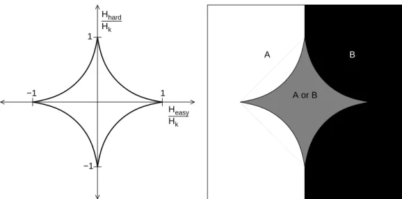
Eq. 2.33 is known as the Stoner-Wolfarth astroid. It gives the two-dimensional hysteresis in magnetic field of a monodomain nanomagnet. Shown in Fig. 2.7(a) is a plot of Eq. 2.33 and shown in Fig. 2.7(b) is a qualitative depiction of hysteretic and non-hysteretic regions. If one traces a path in Heasy-Hhard space into the black region and returns to the gray region,
the magnet will be in state B. Similarly, the magnet can be programmed into state A by tracing a path in Heasy-Hhard space into the white region. State B and A represent θ = 0
and θ = π respectively. One could have readily anticipated the threshold of Hk along the
easy axis from the derivation of the energy barrier in Eq. 2.30.
Finally, in the absence of applied field there is a thermal background energy in the form of spin waves (coherent oscillations of microscopic dipole deviation from the macroscopic
~
M/M direction) and phonons that can cause the magnet to switch between states A and
B, overcoming the energy barrier without the aid of an applied field. Encapsulating these thermal effects by adding a random field term to the dynamical equation for the magnetic moment allows the calculation of a poisson arrival rate of the unwanted thermally-induced switching: [29] λ = fAexp µ −∆U kT ¶ (2.34) Psw = 1 − exp (−λt)
11In both these sources, the problem was solved for uniaxial anisotropy with no easy plane anisotropy (e.g. a prolate spheroid with only shape anisotropy). However, one can argue the same result holds with ˆy
as the hard axis in the oblate ellipsoid (the shape relevant to MRAM nanomagnets), because the easy plane device’s magnetic moment will rest in the z-y plane. Furthermore the application of the field will reduce the energy in the ±ˆy direction depending on the sign of Hhardand not change the location of the new minimum from that of the uniaxial case.
where fA is the attempt frequency and can be approximated as 1GHz for MRAM
appli-cations. [30] To meet retention error rate equirements for a memory product, a barrier of ∆U ≈ 60kT − 70kT is required. Eq. 2.34 and the expression for ∆U in Eq. 2.30 reveal the fundamental scaling challenge of conventional field-switching MRAM: the energy barrier ∆U = 2πM2V (D
b − Dc) scales directly with the cell area (V = (area) · (thickness)) with
all other parameters held constant. To compensate for the decreased amount of magnetic moment, novel materials processing has to be developed to construct larger magnetization
M, or more likely the aspect ratio has to be increased to boost Db− Dc. Yet, either of these
techniques will also increase the field switching threshold Hk = 4πM(Db−Dc), which in turn
translates to a larger current requirement in smaller semiconductor technology nodes. This problem remains for other types of field switching schemes such as toggle switching because
Hk indicates typical field strengths needed to externally control the nanomagnet.
−1 −1 1 H 1 k Hhard Heasy Hk
(a) The two dimensional boundary between bistable region and monostable region in
Heasy-Hhard space.
A or B
A B
(b) A qualitative depiction of how the path through the Heasy− Hhard plane determines the state of the nanomagnet at the origin.
2.3
Magnetization Dynamics
The macroscopic magnetic moment of a ferromagnet is a direct measure of angular mo-mentum with a proportionality factor γ = −|e|/mc, for it is simply the vector sum of the excess electron moments in the majority spin state. Therefore, the definition of torque as the derivative of angular mometnum is applied to explain magnetization dynamics:
d~L dt = ~Γ 1 γ d ~m dt = ~Γ
From Eq. 2.10, the torque from an externally applied field is simply ~m × ~H. Supposing for a
moment that the macroscopic magnetic moment ~m(t = 0) = m0xx+mˆ 0yy +mˆ 0zz experiencesˆ
only the torque from an externally applied field ~H = H ˆz, the solution would be:
~
m(t) = m⊥cos (ωt + ∆φ)ˆx + m⊥sin (ωt + ∆φ)ˆy + mz0zˆ
where m⊥cos (∆φ) = m0x and m⊥sin (∆φ) = m0y. This is in precise agreement with Eq. 2.23
because the ferromagnet’s constituent electron dipole moments are coherently precessing. However, the demagnetization field and other anisotropy energy terms produce an additional, effective field which can be deduced from the angular gradient of Um: [27]
~ HU = 1 m∇U(θ, φ) =~ 1 m · 1 sin θ ∂U ∂φφ +ˆ ∂U ∂θθˆ ¸ (2.35)
Finally, an empirical damping term α is added to complete the equation for magnetization dynamics, known as the Landau-Lifshitz-Gilbert (LLG) equation: [31]
d ~m dt = γ~Γ − α mm ×~ d ~m dt (2.36) d ~m dt = γ ~m × ~H − α mm ×~ d ~m dt (2.37)
To conceptualize the damping process, suppose α ¿ 1 so that d ~m/dt is basically in the
direction of ~m × H. Therefore, the damping term will produce a vector that is perpendicular
to both ~m and ~m × ~H which means the damping produces a tendency for the moment to
fall into alignment with ~H.
2.4
The MTJ structure
pinning antiferromagnet tunneling oxide free layer fixed layers fixed ferromagnet fixed ferromagnet conductive spacerFigure 2.8: A schematic diagram of the stack of materials (Ferromagnet | Oxide | Ferromag-net | Spacer | FerromagFerromag-net | AntiFerromagFerromag-net) that constitutes a MagFerromag-netic Tunnel Junction.
Going from top to bottom, one can understand the purpose of each layer: [7], [32]
1. The free layer stores the bit. It has two possible orientations (indicated by the double arrow): parallel or antiparallel to the fixed ferromagnet magnet immediately below it. 2. The tunneling oxide amplifies the signal in resistance that can be tuned in a wide range from 100Ω to 10kΩ. Without the tunneling oxide, the ferromagnetic materials would produce 1mΩ to 1Ω of resistance because they are conductors.
3. The second ferromagnet is responsible for the magnetization dependent tunneling prob-ability accross the oxide, which translates into two different resistance values when a voltage is applied accross the MTJ.
4. The third ferromagnet helps fix the second ferromagnet by coupling to it through dipole field interactions. Furthermore, this structure can be engineered to produce no net bias magnetic field in the top-most free layer. This is important for ensuring the thermal stability of the free layer and symmetric write characteristics for 1 and 0.
A key figure of merit for the read behavior of an MTJ is its magnetoresistnace ratio:
MR = R1 − R0
R0 (2.38)
where R0 is the lower resistance of the parallel state.
2.5
Spin Angular Momentum Transfer
Spin Angular Momentum transfer is a novel mechanism of switching the free layer in an MTJ without the application of external fields. It is based on the fact that the magnetization of a ferromagnet stems from a preferential population of spin states aligned with the macroscopic magentization. Therefore, passing a current between two ferromagnets suggests that the spin polarized currents will bring their magnetic moment with them and alter the magnetization of the other layer.
z x M1 M2 spin torque −I e− current: y
Figure 2.9: Representation of spin torque due to current between two ferromagnets
The spin torque term is readily attained from arguments based on prior developments in this chapter. Fig. 2.9 describes the coordinate setup for the calculation of the spin transfer torque term. In the figure, current is flowing from ferromagnet 1 to ferromagnet 2. Fer-romagnet 1 can represent the upper ferFer-romagnet in the fixed layer of the MTJ depicted in
Fig. 2.8 and the destination ferromagnet 2 would be the top-most free layer. In order to produce these conditions in an MTJ, a positive voltage at the top of the MTJ would be applied.
The first people to predict this effect, Slonczewski [11] and Berger [33], have described how the change in the macroscopic magnetic moment ∆ ~m2 of the free magnet, on average,
equals the transverse component of one electron’s expected spin magnetic moment < ~µ > (c.f. Eq. 2.20). This is a consequence of the tendency of the spin to align with the macroscopic moment through the intra-atomic exchange interaction. Basically, this treats < ~µ > as a classical vector although individual realizations of ~µ will be ±µB on specific directions of
interaction. This treatment is justified because even the fastest spin transfer switching events reported have involved 106 to 108 electrons. [15], [12]
In order to develop an expression for d ~m2/dt, it is first assumed that every electron in
the switching current is transmitted accross the barrier and has < ~µ >= µBnˆ1 parallel to the
fixed magnet ~m1 = m1nˆ1, where ˆn1 is their common unit vector. The average contribution
of each electron to the change in magnetization is expressed as:
∆ ~m2 = (the projection of < ~µ > onto a plane normal to ~m2)
= < ~µ > − (the projection of < ~µ > onto ~m2)
= µB [ˆn1− (ˆn1· ˆn2)ˆn2] (2.39)
= µB nˆ2× (ˆn1× ˆn2) (2.40)
A vector identity was applied going from Eq. 2.39 to Eq. 2.40 in anticipation of combining this expression with other torque terms in the LLG equation. Intuitively, this vector identity produces the correct magnitude with a µBsin θ term in the inner cross product, and then
produces the correct direction with the outer cross product, by directing ∆ ~m2 such that it