A 220-to-320-GHz FMCW Radar in 65-nm
CMOS Using a Frequency-Comb Architecture
The MIT Faculty has made this article openly available.
Please share
how this access benefits you. Your story matters.
Citation
Yi, Xiang et al. “A 220-to-320-GHz FMCW Radar in 65-nm CMOS
Using a Frequency-Comb Architecture.” IEEE Journal of Solid-State
Circuits (September 2020) © 2020 The Author(s)
As Published
10.1109/JSSC.2020.3020291
Publisher
Institute of Electrical and Electronics Engineers (IEEE)
Version
Author's final manuscript
Citable link
https://hdl.handle.net/1721.1/129442
Terms of Use
Creative Commons Attribution-Noncommercial-Share Alike
A 220-to-320-GHz FMCW Radar in 65-nm CMOS
Using A Frequency-Comb Architecture
Xiang Yi, Senior Member, IEEE, Cheng Wang, Member, IEEE, Xibi Chen, Student Member, IEEE,
Jinchen Wang, Student Member, IEEE, Jes´us Grajal, Member, IEEE, and Ruonan Han, Senior Member, IEEE
Abstract— This paper presents a CMOS-based,
ultra-broadband FMCW (frequency-modulated continuous-wave)
radar using a terahertz (THz) frequency-comb architecture. The high-parallelism spectral sensing provided by this architecture significantly reduces the bandwidth requirement for the THz front-end circuitry and ensures that the peak output power and sensitivity are maintained across the entire band of oper-ation. The speed and linearity of frequency chirping are also improved by the comb system. An antenna-sharing scheme based on a square-mixer-first architecture is used, which not only leads to compact size, but also facilitates the stitching of the multi-channel radar IF data. To avoid the usage of high-cost silicon lens in the on-chip broadband radiation, a multi-resonance substrate-integrated-waveguide (SIW) antenna structure is innovated, which provides 15% fractional bandwidth for impedance matching. As a proof-of-concept, a five-tone radar prototype that seamlessly scan the entire 220-to-320-GHz band is demonstrated. In the measurement, the multi-channel-aggregated EIRP (equivalent isotropically-radiated power) is 0.6 dBm, and is further boosted to ∼20 dBm with a TPX (polymethylpentene) lens. The measured minimum single-sideband noise figure (SSB NF) of the receiver, including the antenna loss and baseband amplifier, is 22.8 dB. Due to the comb-architecture, the EIRP and NF values fluctuate by only 8.8 and 14.6 dB, respectively, across
the 100-GHz bandwidth. The chip has a die size of 5 mm2 and
consumes 840 mW of DC power. This work marks the first CMOS demonstration of THz radar, and achieves record bandwidth and ranging resolution among all radar front-end chips.
Index Terms—FMCW radar, terahertz, CMOS integrated circuit, frequency comb, bandwidth, SIW antenna
I. INTRODUCTION
C
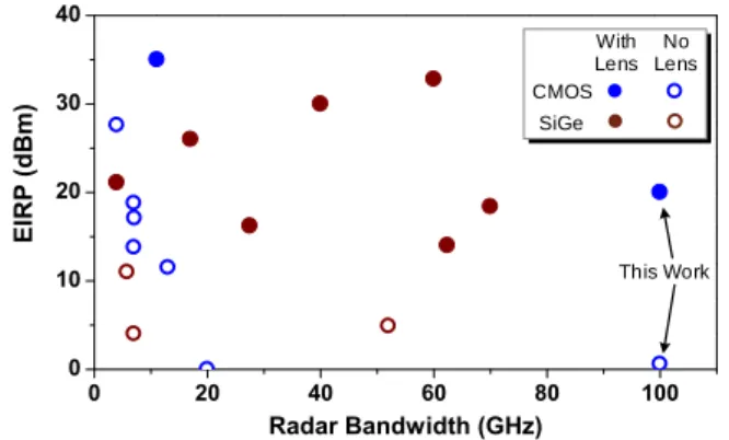
HIP-based radar systems are quickly making their ways to manned/unmanned vehicles, industrial robotics and consumer products, to name a few. In particular, many appli-cations call for significantly increased radar-sensing resolution while keeping the form factor and cost low. That makes radar chips operating in the low-THz regime (∼300 GHz) very attractive. However, it is noteworthy that although such fre-quencies are already >4× higher than that of the mainstream millimeter-wave radars (24 and 77 GHz), the usable bandwidth This is the extended version of a paper originally presented at the IEEE Solid-State Circuit Conference (ISSCC), San Francisco, CA, USA, Febru-ary 2020. This work is supported by the National Science Foundation (CA-REER ECCS-1653100), by MIT Center of Integrated Circuits and Systems (CICS) and by the gift funds from Mitsubishi Electric Research Labs and TSMC.X. Yi, C. Wang, X. Chen, J. Wang, J. Grajal, and R. Han are with the Department of Electrical Engineering and Computer Science, Massachusetts Institute of Technology, Cambridge, MA 02139, USA. X. Chen is also with Tsinghua University, Beiing, China, and J, Grajal is also with Uni-versidad Polit´ecnica de Madrid, Madrid, Spain. E-mail: xiangyi@mit.edu, ruonan@mit.edu. CMOS SiGe With Lens No Lens This Work 0 20 40 60 80 100 0 10 20 30 40 E IRP ( dB m) Radar Bandwidth (GHz)
Fig. 1: A survey of prior millimeter-wave and THz radars using CMOS and SiGe technologies.
is still insufficient for many emerging needs. For example, THz synthetic aperture radars (SAR) have been applied into rapid 3D surface scanning of objects, and a 300-GHz SAR radar with 10-cm synthetic aperture can deliver an azimuth resolution of 1.5 mm for objects placed 30 cm away. However, for a matching ranging resolution, the radar bandwidth should be 100 GHz (i.e. ∼33% fractional bandwidth), which was not demonstrated in prior radars. Similarly, the above millimeter-level resolution is also highly desired for other areas such as high-precision robotics and non-invasive detection of small defects in foam, plastic and rubber products.
Conventional FMCW radars are based on a single-tone architecture and thus provide limited frequency scanning range due to circuit limitations. In particular, for >100-GHz radars, since the operation frequencies are close or even above the cutoff frequencies of the silicon transistors, the related cir-cuit designs need to routinely utilize high-Q resonance for efficiency enhancement. That inevitably reduces the circuit bandwidth. The high carrier frequency also mandates the usage of on-chip antennas, which further aggravates the problem. For front-side radiating structures such as patch antenna, the fractional bandwidth is severely limited to a few percent, due to the short inter-metal-layer distance. Back-side radiating structures such as dipole and slot antennas deliver much higher bandwidth, but require high-cost silicon lens to mitigate the excitation of substrate mode. All these problems cause not only reduction of bandwidth that a radar can cover, but also severe performance degradation at the two edges of the band. A survey of previously reported millimeter-wave and THz radars in silicon are given in Fig. 1. At present, the highest reported FMCW bandwidth is 70 GHz from the 130-nm SiGe radar in
[1]. Excellent equivalent-isotropically-radiated power (EIRP) and noise figure (NF) of 18.4 dBm (with a TPX lens) and 19.7 dB are demonstrated, respectively; they, however, vary by 10.5 dB and 28.6 dB across the 70-GHz bandwidth. Another 55-nm SiGe radar in [2] reduces the EIRP variation to 7.7 dB, but it requires the attachment of a silicon lens, and compared to [1], the achieved bandwidth and EIRP reduce to 62.4 GHz and 14 dBm, respectively. It is also noteworthy that all ultra-broadband radars demonstrated so far are based on high-speed SiGe processes (recently [3] reported a broadband frequency multiplier with 140-GHz bandwidth in 130-nm SiGe process), and low cost CMOS-based radars still operate below 200 GHz and their bandwidths are within 20 GHz. In [4], a 2×2 pulse radar array at 160 GHz is built using a 65-nm CMOS process, and in [5], a FMCW radar at 145 GHz is built using a 28-nm CMOS process; they, however, only deliver bandwidths of 7 GHz and 13 GHz, respectively.
Although the above trade-off between performance and bandwidth seems fundamental, we demonstrate in this paper that a THz-frequency-comb architecture, along with its high-parallelism spectral sensing scheme, are able to optimize both metrics in a scalable manner. As a prototype of this approach, a five-comb-tone radar transceiver, which is originally presented in [6], is implemented using a 65-nm bulk CMOS process. It provides seamless coverage of an entire 220-to-320-GHz band, and the variations of output power and NF in the band are only 8.8 dB and 14.6 dB, respectively. This work not only enables a theoretical bandwidth-limited ranging resolution of 1.5-mm (un-windowed), but also marks the first CMOS demonstration of radars reaching the THz regime. In Section II, the THz-comb architecture, as well as its advantages in radar sensing, are presented. In Section III, details of a few key circuit blocks of the radar are described. In Section IV, characterizations of the electrical performance and ranging resolution of the radar are provided. Finally, in Section V, we conclude the paper with a comparison with prior state-of-the-arts.
II. THZ-COMBRADAR FORBROADBANDSENSING:
CONCEPT ANDCIRCUITARCHITECTURE
Fig. 2 shows the time-variant frequencies of the transmitted (TX) and received (RX) signals in a conventional single-tone FMCW radar with a total bandwidth of BW and chirping duration of Tm. For comparison, the concept of a frequency-comb radar is also shown in Fig. 2. Instead of consecutively scanning the entire bandwidth, it divides BW into N identical segments and sweeps them simultaneously using an array of dedicated transceivers (i.e. channels), which keep equal spac-ing of ∆B=BW /N among their carrier frequencies (hence a frequency comb). As we will show next, each radar transceiver has its own antenna, and the received echo signal is directly mixed with the transmitted signal to generate an IF output. Note that a synthetic bandwidth technique similar to that in Fig. 2 was previously reported in a C-band radar in [7], where the multiple channels are scanned sequentially by a single, tunable transceiver. In our work, the small size of THz circuitry allows for parallel spectral sensing with a monolithic transceiver array. t f Tm BW ΔT=Tm/N N=5 ΔB=BW/N TX signal Echo CH5 CH4 CH3 CH2 CH1 N=5 BW t f t f t f f Comb O utput ΔT
Fig. 2: Broad spectral sensing using simultaneous multi-channel operations in a THz-comb radar architecture.
Target τ t Stitche d IF 2ΔT ΔB ΔT TX Echo t fRF CH i CH i+1 t VIF t VIF CH i CH i+1 fc,i τ C h a n n e l-i T R X IF i C h a n n e l-i+ 1 T R X IF i+1 fc,i+1 φB φA ΔB
Fig. 3: Multi-channel phase coherency in an ideal THz comb radar. The IF data clipping under the over-chirping of the FM signal is also shown (for more details of over-chirping, see Section IV-B).
For a certain channel (e.g. Channel-i), we express the TX signal as:
ST X,i(t) = AT X,icos[(2πfc,i+ π∆Bt
∆T )t + ϕi], (1) where AT X,i and ϕi are the signal amplitude and phase, respectively, fc,i is the frequency at the start of the chirp (t=0), and ∆T =Tm/N is the duration of one chirp (see Fig. 3). Suppose the time-of-flight of wave, determined by the object distance, is τ , the received signal (with an amplitude of ARX,i) for this channel is:
SRX,i(t) = ARX,icos[(2πfc,i+
π∆B(t − τ )
∆T )(t − τ ) + ϕi]. (2) After mixing the above signals, the output IF signal is:
SIF,i(t) = ST X,i(t)SRX,i(t), then, with low-pass filtering =⇒ AT X,iARX,i 2 cos( 2π∆B ∆T τ t + 2πfc,iτ − π∆Bτ2 ∆T ), (3) where π∆Bτ2/∆T is in practice small enough and can be ignored. One key point of (3) is that, the phase of SIF,i(t) is determined by the chirp slope ∆B/∆T , the time-of-flight τ , and the frequency at the start of the chirp fc,i, and
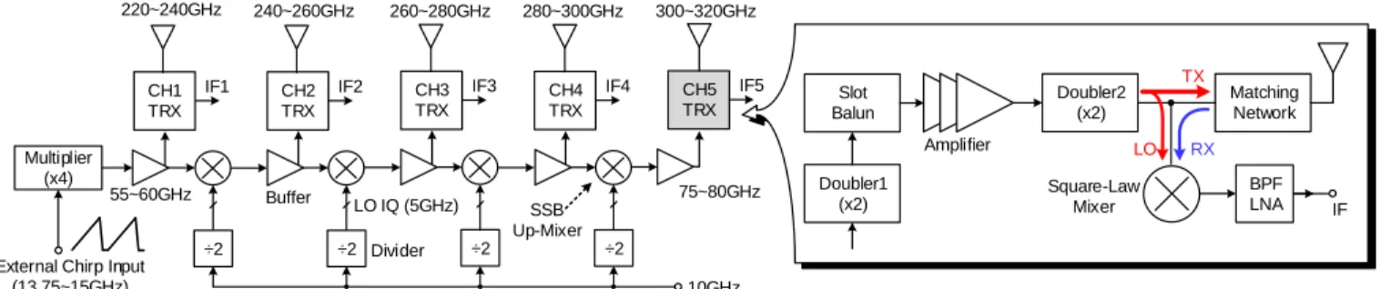
Doubler1 (x2) Doubler2 (x2) Slot Balun Matching Network Square-Law Mixer Amplifier BPF LNA CH2 TRX ÷2 CH1 TRX ÷2 IF1 IF2 10GHz 220~240GHz 55~60GHz Multiplier (x4) CH3 TRX ÷2 IF3 CH4 TRX ÷2 IF4 CH5 TRX IF5 75~80GHz 300~320GHz LO IQ (5GHz) SSB Up-Mixer Buffer 240~260GHz 260~280GHz 280~300GHz Divider IF
External Chirp Input (13.75~15GHz)
TX
LO RX
Fig. 4: The block diagram of the 220-to-320-GHz radar front-end in CMOS.
not dependent on the initial phase of ST X,i, which varies significantly among different channels. Note that ∆B/∆T , τ , and fc,i are all independent with ST X,i. In other words, the phase of IF signal relies on only the chirp slope and starting frequency, as well as the object distance, instead of the initial phase of ST X,i. And the only term varies with channels is the starting frequency fc,i which is a known variable. Therefore, at the end of the chirp (t=∆T ), the phase of the IF signal (ϕA in Fig. 3) becomes:
ϕA= ϕIF,i(t = ∆T ) = 2π∆Bτ +2πfc,iτ = 2πfc,i+1τ. (4) Note that (4) uses the condition fc,i+1=fc,i+∆B, which is accurately realized in our architecture to be shown next. It also shows that the IF phase of Channel-i at the chirp end is identical as the IF phase of Channel-(i + 1) at the chirp start (namely, ϕB=ϕB in Fig. 3). It indicates that, when the multi-channel IF signals are stitched in series (Fig. 3), the result is in theory equivalent to the output expected from a hypothetical single-tone radar with the same total bandwidth of BW =∆B·N .
The comb radar architecture, due to its high-parallelism nature, brings about a few distinct advantages. Firstly, the fractional bandwidth required for each THz-frontend compo-nent (including the on-chip antenna) is relaxed by N times. Correspondingly, high-Q passive structures can be adopted. That also allows for circuit configurations tuned at transistor optimal conditions, such as the maximum available gain near fmax [8]–[10]. Peak circuit performance, therefore, can be maintained across a broad frequency range in a relay manner. We note that although the peak EIRP and minimum NF are normally quoted in the literature on radars, the degraded performance at the band edges ultimately limits the detection distance or speed due to the lower SNR of the amplitude-modulated received signal. The presented scheme effectively improves those “worst-case” merits. Secondly, the comb archi-tecture also significantly relaxes the requirement for the radar chirping frequency synthesizer (e.g. direct-digital synthesizer or DDS). As our radar system (Fig. 4) shows, all on-chip transceivers are referenced to a single synthesizer. So the fractional bandwidth required for the synthesizer is reduced by N times as well. The narrower bandwidth also enables lower power consumption and smaller relative chirped frequency error of the synthesizer. Note that such an error is also not accumulated over different comb channels (but is re-aligned instead) due to the successive frequency upconversion scheme; therefore, the overall linearity of the frequency chirping is
improved by the comb architecture, hence reduced linewidth broadening after the FFT [7]. Thirdly, bandwidth extension is achievable by simply adding more channel transceivers. Such high scalability comes with the expense of larger chip area and power. But due to the compactness of THz components (∼10× smaller than their peers at 77 GHz), we will show that the overall chip area remains acceptable. Also, Fig. 2 shows a N × time reduction for a full-bandwidth scan (for the same SN R), so the total energy consumed by the comb radar remains the same. With higher multi-channel-aggregated EIRP, the scheme is equivalent to the power combining of traditional radars. In fact, due to the aforementioned circuit efficiency enhancement, we in Section IV and V demonstrate that our comb radar consumes less power than many single-tone THz radars.
The block diagram of our 220-to-320-GHz radar front-end is given in Fig. 4, which includes a daisy chain of successive-frequency-upconversion stages. The chain starts from a 13.75∼15-GHz external chirp signal fed into a quadru-pler, and then amplifies the 55∼60-GHz chirp signal and increases its frequency by 5 GHz in each chain stage. To obtain the LO quadrature phases for the single-sideband (SSB) mixer in each stage, the 5-GHz LO is generated by a set of static dividers (÷2) with a 10-GHz input1. If the LO signal and the chirp signal are generated on chip, a cascaded phase-locked loop (PLL) architecture [11] can be used to generate and phase-synchronize the 10-GHz LO signal and the 55∼60-GHz chirp signal [12]. The fact that the 10-55∼60-GHz LO spectrum is directly shifted (rather than multiplied) to the THz output significantly lowers the phase-noise performance requirement for the 10-GHz PLL (compared to that of the 55∼60-GHz PLL), allowing for larger design trade space for this block added to the synthesizer in a conventional radar system. Each stage also drives a THz transceiver, of which the block diagram is also given in Fig. 4. In the case of the fifth channel, the transceiver input at 75∼80 GHz is frequency-doubled twice and is then radiated through an on-chip antenna. In the mean-time, part of the THz signal power, as well as the echo signal received by the same antenna, are also injected into a square-law mixer (details given in Section III-C). Subsequently, the down-mixed IF signal representing the time-of-flight of the THz wave is obtained. Further digitization and processing of the multi-channel IF signals are performed off-chip.
1The off-chip source for the 10-GHz input is synchronized with the
Lslot1 Lslot2 Feed Wcav Lcav Slot Openings
SIW Cavity Sidewall M3~M9 M1-M2 Bottom Layer Al Top Layer Al Top Layer Holes for DRC M1 M2 VIA1 M1-M2 Bottom Layer
Fig. 5: 3D structure of the SIW dual-slot antenna with multi-resonances.
III. DETAILS OFCIRCUITIMPLEMENTATIONS We in this section describe the design details of key circuit blocks, mainly based on Channel-3 without loss of generality. A. SIW-Backed Dual-Slot Antennas with Multi-Resonances
Even though the THz-comb architecture is used, each on-chip antenna should still provide good impedance matching and radiation efficiency across a wide bandwidth of 20 GHz, in order to cover the targeted 100-GHz aggregated band-width. Typically, antenna structures without on-chip ground planes, such as slot and dipole antennas, deliver impedance-matching (S11<-10 dB) fractional bandwidth of >20% [13]. However, they require backside-attached silicon lens to avoid the excitation of substrate mode [2], [14]; that, however, significantly increases the radar cost. Typical silicon lenses, given their small size (<1-cm diameter), also require precise chip antenna alignment with the lens center; such a configu-ration is, however, incompatible with our multi-antenna comb architecture. The on-chip dipole antennas with PCB backside reflectors [15], [16], although offer large bandwidth, require an impractical wafer thinning to <100 µm for ∼300-GHz operations. They also normally have large lateral-direction coupling due to the loosely confined wave in the substrate and tilted radiation beam due to nearby metal structures. In comparison, ground-shielding antennas with front-side radia-tion, such as a patch antenna, mitigate the above problems. But due to the high-Q resonance formed by the closely-spaced top and bottom metal layers, the impedance-matching fractional bandwidth realizable with similar frequency and CMOS process is only 2%∼3% [17]. Moreover, the coupling between two patch antennas is still large when they are placed side-by-side for minimum chip area.
In our chip, an SIW (substrate-integrated-waveguide)-backed dual-slot antenna with multiple resonances is adopted to enable both front-side radiation and wide matching band-width. The 3D structure of the antenna is shown in Fig. 5. In the SIW cavity, M1-M2 shunted layers form the bottom ground plane, M3-to-M9 stack form the four sidewalls, and the top aluminum layer form the upper cavity plane. Holes are dug
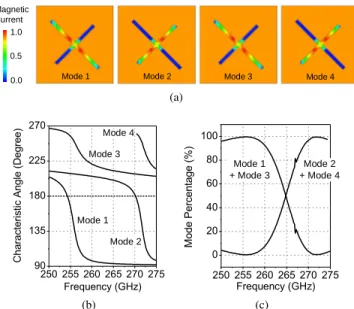
Mode 1 Mode 2 Mode 3 Mode 4 Magnetic Current 0.5 0.0 1.0 (a) 250 255 260 265 270 275 90 135 180 225 270 C ha ra ct er is tic A ng le ( D eg re e) Frequency (GHz) Mode 1 Mode 2 Mode 3 Mode 4 (b) 250 255 260 265 270 275 0 20 40 60 80 100 Mo de P er ce nt ag e (% ) Frequency (GHz) Mode 2 + Mode 4 Mode 1 + Mode 3 (c)
Fig. 6: Simulated characteristic modes of the antenna: (a) the equivalent magnetic current distribution in the slots, (b) the characteristic angles, and (c) mode contributions at varying frequencies.
220 240 260 280 300 320 -20 -15 -10 -5 0 Input M at ching (dB) Frequency (GHz) (a) 250 260 270 280 290 0 10 20 30 40 Efficien cy (%) & A xial Ratio (dB) Frequency (GHz) -20 -15 -10 -5 0 5 Anten na Ga in (dBi) Efficiency Axial Ratio (b) (c) 220 240 260 280 300 -70 -60 -50 -40 -30 Sim u lat e d CH 2 -CH 3 Cou p lin g (dB ) Frequency (GHz) (d)
Fig. 7: Simulated results of the on-chip SIW antenna in Channel 3: (a) input matching (antenna matching network included), (b) radiation efficiency, axial ratio of polarization and antenna gain, (c) radiation pattern, and (d) inter-antenna coupling.
on the bottom and top metal planes to pass the design-rule-check (DRC), and antennas are covered by metal dummy block layers to prevent the dummy metal fillings. In addition, two orthogonal slots are created in the top metal. Since eigenmode analysis is not suitable for lossy, radiative structures, to explain the antenna behavior, analyses based on a characteristic-mode (CM) theory [18], [19] are performed. Using FEKO [20], four antenna characteristic modes are identified, as shown in Fig. 6a, and their characteristic angles (ϕCA) are given in Fig. 6b. Mode 1 and Mode 2 (with ϕCA going across 180◦)
From Buffer (65~70GHz) Vb1 C1 TL1 M1 M2 M3 TL2 TL3 TL4 VDD To Balun TF1 Vb2 VDD (a) 120 130 140 150 -40 -35 -30 -25 -20 -15 -10 -5 0 C on ve rs io n G ai n (d B ) Output Frequency (GHz) (b) 120 130 140 150 -60 -50 -40 -30 -20 -10 0 10 D ou bl er 1 Ou tp ut P ow er ( dB m) Output Frequency (GHz) (c)
Fig. 8: (a) Schematic of Doubler 1 inside the radar transceiver. (b) Simulated
doubler conversion gain at varying output frequency (Pin=2 dBm). (c)
Simulated doubler output power (the input power variation from the preceding circuitry is also included).
are associated with the resonances of the longer and shorter slots, respectively; Mode 3 and Mode 4 (with ϕCAbeing non-180◦ but exhibiting dramatic change), which are originated from the resonance of the SIW cavity, are the parasitic modes of Mode 1 and Mode 2, respectively.
By adjusting Lslot1 and Lslot2 in Fig. 5, we position the resonance frequencies of Mode 1 and Mode 2 at the two sides of the radar channel band; in addition, tuning Wcav, Lcav (hence Mode 3 and Mode 4) further flattens the off-resonance impedance change. These efforts eventually lead to a broad impedance-matching bandwidth from 250 GHz to 290 GHz (i.e. 15% fractional bandwidth), as the simulation in Fig. 7a shows. Also note that the radiated waves from Mode 1 & 3 and Mode 2 & 4 are linearly polarized in two orthogonal directions. Therefore, as the contribution of each mode varies with frequency (Fig. 6c), the polarization of the overall radiated field rotates2. The simulated antenna pattern is shown in Fig. 7c, which has a gain of -1∼0 dBi across the 260∼280-GHz band. Lastly, Fig. 7d indicates that, due to the high confinement of the resonance wave in the metal cavity, as well as the difference of antenna center frequencies, the inter-antenna coupling is weak (<-31 dB).
B. THz Transmitter Chain
The schematic of Doubler 1 of the THz transceiver is shown in Fig. 8a. The millimeter-wave signal from the frequency conversion chain drives a common-source buffer (M1) and is then turned into differential mode through a single-loop
2This is different from circular polarized waves, which is undesired for our
TX-RX antenna sharing scheme. Since the antenna feed in Fig. 5 aligns with the centers of both slots, the radiated fields in the two orthogonal directions are always in-phase. The polarization of the total radiation is therefore always linear, as the >11.6-dB simulated axial ratio in Fig. 7b indicates.
λ/4 Slot Resonators IN OUT Electrical Field Microstrip Forward Current Microstrip Return Current (a) 100 120 140 160 -15 -10 -5 0 S -P ar am et er s (d B ) Frequency (GHz) S21 & S31 -3dB S11 (b) 100 120 140 160-0.1 0.0 0.1 0.2 0.3 Ph ase Imba lance (Deg ree ) Frequency (GHz) A mp lit ud e Imb al an ce ( dB ) -0.04 -0.03 -0.02 -0.01 0.00 (c)
Fig. 9: (a) The 3D structure of the 135-GHz slot-based balun. (b) Simulated insertion loss (S21and S31) and return loss (S11). (c) Simulated phase and
amplitude imbalance at the differential outputs.
transformer (T F1). A push-push structure is then used to generate the second-harmonic component while suppressing the tone at input frequency. Shown in Fig. 8b and Fig. 8c, the peak conversion gain and output power of Doubler 1 are -2 dB and 0.7 dBm, respectively. The simulated DC power of the entire circuit in Fig. 8a is 21 mW.
As shown in Fig. 4, before the second frequency-doubling in the THz transceiver, the signal from Doubler 1 is converted to differential mode using a slot balun (Fig. 9a) and is boosted by a chain of amplifiers (Fig. 10a). Since the amplifiers are based on a pseudo-differential topology with a neutralization technique (details to be given next), they are sensitive to any amplitude and phase imbalance of the input signal. To minimize such imbalance, a sub-THz balun structure based on a pair of folded slot resonators [21] is adopted. Shown in Fig. 9a, the balun input and output consist of a single-ended microstrip line and a pair of differential microstrip lines, respectively. A gap in the ground plane couples the input and output; it is also enclosed by two pairs of quarter-wavelength slot resonators which present high impedance on the two ends of the ground gap. The resonators are folded for compact size and minimum radiative loss. With the excitation by the single-ended signal in the input microstrip, only a fully-differential quasi-TE mode wave is allowed in the ground gap [22]. Meanwhile, since the microstrip pair and the slot resonators at the output side are completely symmetric, when the above quasi-TE wave is coupled back to microstrip mode, the generated output signals are expected to keep perfect out-of-phase balance across a wide range of frequency. Our full-wave electromagnetic simulation shows that the insertion loss
Cascaded Neutralized Amplifier IN Doubler2 To RX To MN (a) 120 130 140 150 -10 -5 0 5 10 A mp lif ie r Ga in ( dB ) Frequency (GHz) (b) 250 260 270 280 290 -40 -30 -20 -10 0 10 D ou bl er Ou tp ut P ow er ( dB m) Frequency (GHz) (c)
Fig. 10: (a) Schematic of Doubler 2 and its input amplifier inside the THz radar transceiver. (b) Simulated gain of the cascaded neutralized amplifier chain including the input slot balun. (c) Simulated output power of Doubler 2 with an input power of -1 dBm.
of the balun is 1.3 dB (Fig. 9b) and the amplitude/phase imbalance across a 100∼160-GHz band is negligible (Fig. 9c). The signal generated by the slot balun is then amplified by three identical, pseudo-differential amplifier stages, shown in Fig. 10a. The stages are coupled through central-tapped transformers. In each stage, a cross-coupled capacitor pair (e.g. C4and C5) is used to create negative capacitance that cancels the Cgdof the transistors. Although this neutralization scheme does not provide the highest possible gain compared to the techniques in [8]–[10], [21], the device unilaterization that this scheme enables allows for higher stability and broader bandwidth [23]. The simulated gain of the amplifier chain is shown in Fig. 10b, with an average value of ∼7 dB in the 130∼140-GHz band. Finally, the TX signal is frequency doubled again by a pair of push-push transistors (M10 and M11). The inductive reactances provided by transmission lines T L7 and T L8 boost the swing of the device drain voltages (hence higher nonlinearity), and T L9 and T L10 are used as part of the output matching network. In the simulation, the amplifier chain and Doubler 2 consume DC power of 57 mW and 24.8 mW, respectively, and the final TX output power (as shown in Fig. 10c, is -5∼-1.5 dBm at 260∼280 GHz. C. THz Receiver Chain
Most of previous chip radars employ separate antennas for the TX and RX [2], [4], [5]. Such a configuration, however, is not desirable in our comb architecture; because the integration of the associated on-chip antennas requires exceedingly large die area. In comparison, antenna sharing between TX and RX significantly reduces chip area, but the direct injection of the large power TX signal into RX causes severe nonlinearity or even saturation of the RX low-noise amplifier. To mitigate
IF VDD From TX & Antenna Vb2 BPF + LNA TL18 TL19 C10 C11 R1 M12 M13 M13 Square-Law Mixer R2 R3 R4 Cgd Rch ich,LPF C12 (a) 240 260 280 300 15 20 25 30 35 N oi se F ig ur e (d B ) Frequency (GHz) (b) 240 260 280 300 10 15 20 25 R ec ei ve r G ai n (d B ) Frequency (GHz) (c)
Fig. 11: (a) The schematic of the THz radar receiver chain, (b) simulated SSB noise figure of the square-law mixer, and (c) simulated conversion gain of the receiver chain. The IF frequency in the simulation is 3 MHz.
Buffer Multiplier (X4) Vb To Next Buffer LOI+LOI- LOQ+ LO Q-I+ Q+ Q- I-To CH1 TRX I+ I- Q+ Q-SSB Up-Conversion Mixer 13.75~15GHz FMCW 55~60GHz 60~65GHz
Fig. 12: Schematics of input multiplier (X4), buffer, and SSB mixer.
this problem, a circularly-polarized antenna cascaded with a directional coupler is used in the SiGe radar in [14]. Since the operation frequency of our radar has exceeded the transistor speed limit of the 65-nm CMOS process used here (fmax=280 GHz), a pre-amplifier in the RX front-end would not be possible, and the radar echo signal can only be directly down-converted. Although this passive-mixer-first architecture has degraded sensitivity (i.e. lower conversion gain and higher noise figure), its high linearity also makes the above antenna-sharing scheme possible.
The schematic of the radar receiver of one channel is given in Fig. 11a, where a unique square-law mixer topol-ogy is adopted. The mixer is based on a MOSFET (M12) with zero drain bias (VD=0 V) and sub-threshold gate bias (VG=Vb2=0.28 V <VT). The channel resistance Rch therefore changes exponentially with the instantaneous gate voltage (Vg=VG+vg): Rch= Rch0· e VT −Vg nφt = Rch0· e VT −VG−vg nφt , (5)
where n is the ideality factor (close to unity), φtis the thermal voltage (26 mV at room temperature) and Rch0 is the channel resistance at Vg=VT. Next, we note that at THz frequencies, the AC voltages at gate and drain are similar (vg≈vd) due to the parasitic capacitance Cgd between the two terminals.
Therefore, the channel current is: ich ≈ vg Rch = vg Rch0· e VT −VG−vg nφt =e VG−VT nφt Rch0 vg· e vg nφt (6) ≈e VG−VT nφt Rch0 (vg+ v2 g nφt ), (7)
In Fig. 11a, the second-order term in (7) is used for RX down-conversion: by directly superposing the TX and echo signals on the device gate (vg=vT X+vRX), an IF signal (fIF=fT X -fRX) carrying the object distance information is obtained:
iIF =
eVG−VTnφt nφtRch0
|vT XvRX| cos [(ωT X− ωRX)t + ϕIF]. (8) The presented THz square-law mixer well fits the antenna-sharing architecture and consumes zero DC power. Its fully passive condition not only accommodates large input power, but also provides an output with minimum flicker noise [24]. The latter is particularly important for short-range THz radars, of which the generated IF frequency is normally low. In the simulation, the mixer has a P1dB of -5.5 dBm, and a single-sideband noise figure (SSB NF) of 20.6∼23.6 dB in the 260∼280-GHz band (Fig. 11b). Following the mixer is a two-stage, self-biasing baseband amplifier, which has 3.3-nV/Hz1/2 simulated input-referred noise (lower than the mixer output noise) and enables an overall conversion gain of 21∼21.7 dB for the receiver chain (Fig. 11c). An R-C high-pass filter is added between the THz mixer and the baseband amplifier, in order to suppress any unwanted low-frequency IF signal caused by the reflections at objects (e.g. bond wires) in close proximity to the chip. It also filters out the low-frequency components due to the power fluctuation of the THz LO signal during chirping (see Section IV-B), which is also down-converted by the THz square-law mixer.
D. Successive Frequency-Conversion Chain
Between radar channels, the frequency conversion for each THz transceiver input is realized by a buffered SSB mixer (Fig. 12). To generate the RF I-Q signals for the mixer, a set of broadband and compact R-C polyphase filters are adopted. The loss of the filters is compensated by a chain of common-source amplifiers in each stage. Each SSB mixer increases the frequency by 5 GHz, and the 5-GHz mixer I-Q LO signals are generated from a digital divider (÷2) clocked at 10 GHz. At the input of the frequency conversion daisy chain, two push-push frequency doublers that are cascaded through a transformer are used to convert the input FMCW signal at 13.75∼15 GHz to 55∼60 GHz.
The spurs due to the successive frequency-conversion chain may be of concern. These spurs with 5-GHz frequency spacing derive from the SSB mixer due to the RF and LO I-Q imbalance. The measured spurs are about 39 dB lower than the THz transmitted signal. Besides, antenna coupling between channels generates leakages. All spurs and leakages are down-converted by the square-law mixer, and then generate DC due to the self-mixing and (m · 5 GHz) out-of-band IF signals, where m is the integer. As shown in Fig. 11a, the DC due to
SIW Antenna 2.0 mm 2.5 mm Buffer MixerSSB Divider Doubler1 Balun Amplifier Multiplier(X4) RX Doubler2 Matching Network (a) Wire-Bonded Chip (b) (c)
Fig. 13: The photos of (a) the 220-to-320-GHz CMOS radar, (b) the wire-bonded chip on a PCB, and (c) the chip package with a front-side TPX lens.
the self-mixing is blocked by the R-C high-pass filter. The low-pass output characteristic of the square-law mixer suppresses the out-of-band IF signals. The simulated out-of-band input P1dB of the whole receiver limited by the square-law mixer is -5.5 dBm, which is higher than the power of spurs and leakages. Therefore, all spurs and leakages do not affect the receiver.
IV. MEASUREMENTRESULTS
The 220-to-320-GHz comb radar is implemented using TSMC 65-nm bulk CMOS technology, and its die photo is shown in Fig. 13a. The chip occupies an area of 2×2.5 mm2. For testing, the chip is mounted on a PCB with standard wire bonding (Fig. 13b). As Fig. 13a shows, the bond pads are placed away from the on-chip antennas with the largest possible distance, in order to minimize the radiation interference from the bond wires. To enhance the antenna directivity, a detachable low-cost TPX polymethylpentene lens (diameter=25.4 mm, focal length=10 mm) is placed at the front side of the chip (Fig. 13c). The measured total power consumption of the CMOS radar chip is 0.84 W.
A. Characterization of Electrical Performance
In this part of the measurement, the RF input of the chip is provided by an external signal generator with no FM chirp-ing, and each THz transceiver can be activated/de-activated independently. The performance of the chip transmitter mode
VDI Extender (Receiver) Signal Generator (E8257D) Signal Generator (N5173B) Horn Antenna LO 10GHz 13.75~15GHz RF PCB Spectrum Analyzer (N9020A) Signal Generator (83732B) LO IF Lens (w/, w/o) (Calibrated by PM5) VDI Erickson PM5 Powermeter (a) VDI Extender (Transmitter) Signal Generator (E8257D) Signal Generator (N5173B) Horn Antenna LO 10GHz 13.75~15GHz RF PCB Signal Generator (83732B) Spectrum Analyzer (N9020A) IF RF
Output Power Calibrated by PM5 Lens (w/, w/o)
(b)
Fig. 14: Measurement setups for RF performance of (a) TX and (b) RX.
is measured using the set-up shown in Fig. 14a. First, we use a horn antenna (Gant≈25 dBi), a VDI WR-3.4 VNA (vector network analyzer) frequency extender (configured in receiver mode), and a spectrum analyzer to down-convert and measure the radiated waves of the chip. Since the polarization directions of the SIW-backed dual-slot antennas rotate with frequency, the measured output power by placing the horn antenna vertically and horizontally are added together. Shown in Fig. 15a is the measured power at varying distance d between the chip (without the TPX lens) and the VDI extender. Note that a VDI Erickson PM5 powermeter is also used to calibrate the conversion loss of the VDI extender across the WR-3 band, and to directly measure the radiated power for d<5 cm as a cross check. Fig. 15a indicates that beyond the far-field limit of ∼3 cm, the results match the Friis equation [25] well, and the calculated EIRP is around -10 dBm. In Fig. 15b, the phase noise of all channel outputs measured by down-converting them into IF signals are shown. At 1-MHz offset, the phase noise, which is mainly limited by the multiplied phase noise of the LO signal for VDI extender, is about -100 dBc/Hz on average. In Fig. 15c, the measured radiation pattern of the chip (Channel-3), again without the TPX lens, is shown, which has a 3-dB beamwidth of ∼90◦ and well matches the simulated result in Fig. 7c. Lastly, by turning on the THz transceivers one-by-one and by sweeping the input RF frequency (13.75∼15 GHz), the measured EIRP of each channel is shown in Fig. 16. The peak multi-channel-aggregated EIRP of the radar3(without lens) is 0.6 dBm, and it is evident that with the THz comb architecture, the fluctuation of the EIRP across the entire 100-GHz bandwidth is only
3Although the output waves of the channels are not coherent, the
multi-channel aggregated EIRP is still a meaningful metric for a fair comparison with prior single-tone radars, in terms of the equivalent signal-to-noise ratio (with the same integration time), detection distance and energy efficiency.
0.5 1 2 4 8 16 32 -55 -50 -45 -40 -35 -30 -25 -20 Measured Pow er (d Bm ) Distance (cm) 1/Distance2 No TPX Lens (a) 0.1 1 10 100 1000 -120 -100 -80 -60 -40 -20 M ea sur ed T X Pha se Noi se (d Bc /Hz ) Frequency Offset (kHz) (b) -90 -60 -30 0 30 60 E-Plan e H-Plan e 0dB -10dB (c)
Fig. 15: (a) Power received by the VDI VNA extender at varying distance. (b) Measured TX phase noise of the radar. (c) Measured TX radiation pattern without the TPX lens. Note that these results are from Channel 3 of the chip.
200 220 240 260 280 300 320 340 -60 -40 -20 0 20 Me as ured EIRP ( dBm ) Frequency (GHz) CH1 CH2 CH3 CH4 CH5
Fig. 16: Measured EIRP of each radar channel with (solid line) and without (dash line) the TPX lens.
8.8 dB. With the TPX lens, the multi-channel aggregated EIRP increases significantly to ∼20 dBm.
Next, to measure the detection sensitivity of the radar chip, a setup illustrated in Fig. 14b is used. The VDI WR-3.4 VNA extender is configured in transmitter mode and its output radiated from a horn antenna is again calibrated by the Erickson PM5 powermeter. The IF output (fIF=4 MHz) of each radar channel is measured by a spectrum analyzer. Again, the measured output power by placing the horn antenna vertically and horizontally are added together. To quantify the conversion gain of the chip receiver, we derive the radiation power impinging on each chip antenna as:
PR|dBm= PT X|dBm+ GT X,ant|dBi+ 20 log10 λ
4πd + DR|dBi, (9) where PT X and GT X are the output power and antenna gain
200 220 240 260 280 300 320 340 -50 -40 -30 -20 -10 0 10 20 30 Frequency (GHz) G ai n (d B) 20 30 40 50 60 70 80 90 100 Noi se F ig ure (d B) CH1 CH2 CH3 CH4 CH5
Fig. 17: Measured conversion gain (dash lines) and SSB noise figure (solid lines) of each radar channel without the TPX lens.
of the VDI extender source, and DR is the directivity of the chip antenna (7 dBi). The conversion gain of each receiver channel is therefore:
GC|dB= PIF|dBm− PR|dBm, (10) where PIF is the IF output power of the chip. Based on (10), the measured results without using the TPX lens is shown in Fig. 17. Note that this conversion gain, with a peak value of 22 dB, includes the amplification of the receiver baseband buffer and the antenna efficiency of ∼20%. Lastly, the baseband output noise floor PN of each receiver channel is measured, which then gives the single-sideband noise figure (SSB NF) of the chip by using the gain method:
N F |dB= PN|dBm/Hz− (−174|dBm/Hz) − GC|dB, (11) which is plotted in Fig. 17. The minimum measured NF (again including the baseband amplifier and antenna loss) is 22.2 dB, and its fluctuation across the 100-GHz bandwidth is 14.6 dB. B. Radar Demonstration and Characterization
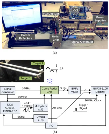
To realize ranging detection, the input FMCW chirp signal is generated by a DDS (AD9164-FMCB-EBZ) and a multiplier chain as shown in Fig. 18b. The five radar IF outputs are acquired synchronously by a multi-channel digitizer (NI PXI-5105) and then calibrated and stitched by Matlab in a PC. Similar to the operation of conventional FMCW radars, over-chirping is applied in the generation of the sawtooth FM signal in the DDS to ensure that the entire channel bandwidth (∆B=20 GHz in Fig. 3) is covered without the impact of the ramping-down portion of the sawtooth signal. Accordingly, in Matlab, the IF data sections outside the duration of ∆B is clipped off (Fig. 3). Note that the IF stitching in Fig. 3 only requires precise ∆B and ∆T ; such conditions are ensured by the global 10-MHz clock signal in Fig. 18b, which synchro-nizes the DDS (with a DDS chirping slope of 625 MHz/µs) and the PXI digitizer (with ∆T =32 µs). Also note that (4) in Section II shows the starting points of the ∆T clipped sections of IF data do not need to be precise; they only need to be identical across all five channels.
Similar to conventional FMCW radars, signal calibration is applied before the IF stitching, in order to correct a few systematic non-idealities associated with the circuit implemen-tation. Firstly, due to the fluctuations in TX power (Fig. 16)
Corner
Reflectors Radar Chip PXI Digitizer DDS Signal Generator Power Supplies (a) DDS AD9164-FMCB-EBZ Multipliers (x4) Comb Radar Chip 3.44~ 3.75GHz NI PXI-5105 Digitizer 5 IFs Signal Generator 10GHz BPFs VGAs Divider (÷N) 10MHz 5GHz Trigger Signal PC 10MHz Clock ΔR Target 1 Target 2 Arduino (b)
Fig. 18: (a) The photo and (b) the block diagram of the setup used for the testing of radar ranging capability.
and RX gain (Fig. 17), the IF signal strength has non-flat frequency response inside each channel and mismatches among different channels; that results in amplitude modulation of the IF signal during chirping and spectrum broadening after performing the FFT [26], [27]. Secondly, there are two sources of delay (phase) mismatches among the channels: one is from the antenna and matching network, and the other one is from the different locations of antennas on the chip. The latter can be ignored when the object is right in the front of radar and with sufficiently large distance (>20 cm). To detect objects in other directions, a phase gradient similar to that in a linear phased array should be applied. Thirdly, any chirp nonlinearity will also cause IF spectrum broadening [28]. Finally, the amplitude fluctuations of TX signal can be directly rectified and down-converted by the square-law mixer in the RX, and generate a low-frequency false signal; fortunately, it can be filtered out by the high-pass filter in the RX as mentioned before. To address the aforementioned gain and phase mismatches, as well as the spectrum-broadening problems, a calibration method derived from [28] and shown in Fig. 19a is adopted. A single-point-like target (i.e. a corner reflector in our experiment) is used as the reference target to generate the calibration data for each channel. Assume Sref,i(t) is the Hilbert transform of the ith-channel reference IF signal, the ith-channel calibration data Scal,i is
Scal,i(t) = Sref,i(t) · e−j(2πfIFt+2πfIF∆T (i−1)+ϕ1), (12) where fIF is the mean target frequency of Sref, and ϕ1is the phase of Sref,1. Therefore, the aforementioned non-idealities
Calibrat ion Raw Data Reference Target Calibrat ion Data IF Stitching ,( ) ref i t S Scal i,( )t ( ) it S ,( ) raw i t S (a) 0 1000 2000 3000 4000 -2 -1 0 1 2 VIF (a. u. )
Index of Data Points
CH 1 CH 2
(b)
Fig. 19: (a) FMCW radar signal calibration process. (b) Example of a section of calibrated and stitched data for two corner reflectors spaced with a distance of ∆R=19 mm.
of raw data, Sraw,i, can be one-time calibrated by Scal,i, and the calibrated IF signal is
Si(t) = Sraw,i(t)/Scal,i(t). (13) Finally, the calibrated IF signals are stitched in the time domain.
A set of corner reflectors are measured to verify the IF stitching process after the signal calibration. Fig. 19b shows the waveform of two corner reflectors with the data of two radar channels. It can be seen that, the modulated envelope of IF signal, which stems from two closely spaced IF tones representing the two objects, is continuous over the stitched channels; the extended periods of that envelope (hence higher FFT resolution) due to stitching, therefore, helps distinguishing those two tones in the IF spectrum. Two corner reflectors are used to measure the range resolution of the comb radar. In order to see the two separated spectrum peaks clearly with 100-GHz bandwidth and Hamming window (broadening factor is 1.5), these two corner reflectors have 2.5-mm range difference, so the corresponding separable range difference without windowing is 1.67 mm. Fig. 20 illustrates the improvement of the range resolution in comb radar: a single channel (BW =20 GHz, Fig. 20a) is unable to resolve the objects; with the stitching of three adjacent channels (BW =60 GHz, Fig. 20b), the object separation starts to show; and with all five channels stitched together (BW =100 GHz, Fig. 20c), the separation becomes distinct. It also indicates that the resolution limit is still not reached in Fig. 20c. The linewidth of the windowed IF lobe corresponds to a value very close to the theoretical windowed resolution of 2.25 mm, or theoretical bandwidth limited resolution of 1.5 mm.
Lastly, the accuracy of the ranging detection is measured by using one corner reflector at varying distance of 30∼200 cm on a linear stage. As shown in Fig. 21, the measured values agree well with the real distances. The range accuracy with
29.5 30.0 30.5 31.0 31.5 32.0 32.5 33.0 -40 -30 -20 -10 0 N or m ali ze d P ow er (d B ) Range (cm) 1 CH (a) 1 CH 29.5 30.0 30.5 31.0 31.5 32.0 32.5 33.0 -40 -30 -20 -10 0 N or m ali ze d P ow er ( dB ) Range (cm) 3 CH (b) 1 CH 3 CH 29.5 30.0 30.5 31.0 31.5 32.0 32.5 33.0 -40 -30 -20 -10 0 N or m ali ze d P ow er ( dB ) Range (cm) 5 CH (c)
Fig. 20: Measured FFT results (Hamming window) of two corner reflectors (∆R=2.5 mm) with IF data from (a) one, (b) three, and (c) five channels.
0 50 100 150 200 0 50 100 150 200 M e a s u re d D is ta n c e ( cm ) Real Distance (cm) Ideal Curve Measured Distance 31.0 31.5 32.0 31.5 32.0
Fig. 21: Measured ranging accuracy of the comb radar.
0.32-ms integration time is within 0.2 mm which is limited by the reference rule.
V. CONCLUSION
Although it is challenging to achieve high fractional band-width in THz sensing microsystems, the circuit down-scaling due to the increasing frequency opens up the opportunity in a single-chip integration of multi-tone transceiver arrays for high-parallelism spectral coverage. Such a comb archi-tecture breaks the conventional trade-offs among bandwidth, performance and efficiency. The radar chip presented in this paper showcases that advantage. TABLE I summarizes its performance and comparisons with the other state-of-the-art
TABLE I: SUMMARY OF THECHIPPERFORMANCE ANDCOMPARISON WITHOTHERSTATE-OF-THE-ARTBROADBANDRADARS INSILICON
References Technology Frequency
(GHz) Bandwidth (GHz) Resolution (mm)(a) Output EIRP (dBm) Minimum NF (dB) EIRP & NF Fluctuation (dB) Chip Size (mm2) DC Power (mW) T-THz 2018 [1] 130-nm SiGe 305∼375 70 2.1 6, 18.4 (b) 19.7 10.5 & 28.6 2.85 1700 T-MTT 2019 [2] 55-nm SiGe 189.9∼252.3 62.4 2.4 14 (c) NA 7.7 & NA 0.51 87 JSSC 2014 [4] 65-nm CMOS 157.9∼164.9 7 21 18.8 22.5 3 & NA 20 2200 ISSCC 2019 [5] 28-nm CMOS 138∼151 13 11.5 11.5 4 (d) 1.5 & 4 6.5 500 T-THz 2016 [14] 130-nm SiGe 210∼270 60 2.5 32.8 (c) 21 20 & 29 3.2 1800 This Work 65-nm CMOS 220∼320 100 1.5 0.6
(e), 20(e) 22.2 8.8 & 14.6 5 840
(a)Theoretical resolution determined by c
2·BW (c: speed of light).
(b)With TPX lens. (c)With silicon lens. (d)Effective isotropic NF including the antenna directivity. (e)Multi-channel aggregated EIRP.
broadband radars in silicon. This work marks the first CMOS implementation of FMCW radars operating above 200 GHz, as well as the largest bandwidth. More importantly, although the SiGe counterparts [1] and [14] have wide bandwidth and high EIRP, their EIRP and NF fluctuation are higher than that of the presented radar which are 8.8 dB and 14.6 dB across the 100-GHz bandwidth, respectively.
The presented THz-comb sensing scheme multiplies the amount of hardware (amplification, filtering, data sampling, etc.) needed at the baseband. But due to the increased equiva-lent FMCW chirping speed, the overall energy efficiency is not degraded. This additional hardware overhead is also expected to significantly shrink with more advanced CMOS technology nodes. Note that the fmax of the 65-nm CMOS process used in this work is only 280 GHz; with the recent development of FinFET (fmax=450 GHz in [29]) and FDSOI (fmax=370 GHz in [30]) CMOS technologies, the EIRP and NF are expected to improve significantly, too, which further make low-THz radar sensing more practical for emerging applications that require higher resolution and smaller form factor.
ACKNOWLEDGMENT
The authors would like to thank TSMC University Shuttle Program for the chip fabrication, and thank Muting Lu, Qingyu Yang, Nathan Monroe, Mohamed I. Ibrahim (MIT), Pu Wang, and Rui Ma (Mitsubishi Electric Research Labs) for their helps on the measurement. The authors also appreciate Dr. Jenshan Lin at the National Science Foundation (NSF) for his support.
REFERENCES
[1] J. Al-Eryani, H. Knapp, J. Kammerer, K. Aufinger, H. Li, and L. Maurer, “Fully Integrated Single-Chip 305-375-GHz Transceiver with On-Chip Antennas in SiGe BiCMOS,” IEEE Transactions on Terahertz Science and Technology, vol. 8, no. 3, pp. 329–339, 2018.
[2] A. Mostajeran, S. M. H. Naghavi, M. Emadi, S. Samala, B. P. Gins-burg, M. Aseeri, and E. Afshari, “A High-Resolution 220-GHz Ultra-Wideband Fully Integrated ISAR Imaging System,” IEEE Transactions on Microwave Theory and Techniques, vol. 67, no. 1, pp. 329–339, 2019. [3] A. Ali, J. Yun, M. Kucharski, H. J. Ng, D. Kissinger, and P. Colantonio, “220-360-GHz Broadband Frequency Multiplier Chains (x8) in 130-nm BiCMOS Technology,” IEEE Transactions on Microwave Theory and Techniques, 2020.
[4] B. P. Ginsburg, S. M. Ramaswamy, V. Rentala, E. Seok, S. Sankaran, and B. Haroun, “A 160 GHz Pulsed Radar Transceiver in 65 nm CMOS,” IEEE Journal of Solid-State Circuits, vol. 49, no. 4, pp. 984–995, 2014. [5] A. Visweswaran, K. Vaesen, S. Sinha, I. Ocket, M. Glassee, C. Desset, A. Bourdoux, and P. Wambacq, “A 145GHz FMCW-Radar Transceiver in 28nm CMOS,” in IEEE International Solid- State Circuits Conference (ISSCC), 2019, pp. 168–170.
[6] X. Yi, C. Wang, M. Lu, J. Wang, J. Grajal, and R. Han, “A Terahertz FMCW Comb Radar in 65nm CMOS with 100GHz Bandwidth,” in IEEE International Solid-State Circuits Conference (ISSCC), 2020, pp. 90–92.
[7] S. Balon, K. Mouthaan, C. H. Heng, and Z. N. Chen, “A C-Band FMCW SAR Transmitter with 2-GHz Bandwidth Using Injection-Locking and Synthetic Bandwidth Techniques,” IEEE Transactions on Microwave Theory and Techniques, vol. 66, no. 11, pp. 5095–5105, 2018. [8] R. Spence, Linear Active Networks. John Wiley & Sons Ltd, 1970. [9] Z. Wang and P. Heydari, “A Study of Operating Condition and Design
Methods to Achieve the Upper Limit of Power Gain in Amplifiers at Near-fmax Frequencies,” IEEE Transactions on Circuits and Systems I: Regular Papers, vol. 64, no. 2, pp. 261–271, 2017.
[10] H. Bameri and O. Momeni, “A High-Gain mm-Wave Amplifier Design: An Analytical Approach to Power Gain Boosting,” IEEE Journal of Solid-State Circuits, vol. 52, no. 2, pp. 357–370, 2 2017.
[11] D. Park and S. Cho, “A 14.2 mW 2.55-to-3GHz Cascaded PLL with Reference Injection, 800MHz Delta-Sigma Modulator and 255fs rms Integrated Jitter in 0.13 µm CMOS,” in IEEE International Solid-State Circuits Conference, 2012, pp. 344–346.
[12] J. Lee, Y.-A. Li, M.-H. Hung, and S.-J. Huang, “A Fully-Integrated 77-GHz FMCW Radar Transceiver in 65-nm CMOS Technology,” IEEE Journal of Solid-State Circuits, vol. 45, no. 12, pp. 2746–2756, 2010. [13] R. Han and E. Afshari, “A CMOS High-Power Broadband 260-GHz
Radiator Array for Spectroscopy,” IEEE Journal of Solid-State Circuits, vol. 48, no. 12, pp. 3090–3104, 2013.
[14] J. Grzyb, K. Statnikov, N. Sarmah, B. Heinemann, and U. R. Pfeiffer, “A 210-270-GHz Circularly Polarized FMCW Radar with a Single-Lens-Coupled SiGe HBT Chip,” IEEE Transactions on Terahertz Science and Technology, vol. 6, no. 6, pp. 771–783, 2016.
[15] S. Yuan and H. Schumacher, “110–140-GHz Single-Chip Reconfigurable Radar Frontend with On-Chip Antenna,” in IEEE Bipolar/BiCMOS Circuits and Technology Meeting-BCTM, 2015, pp. 48–51.
[16] H. J. Ng, M. Kucharski, W. Ahmad, and D. Kissinger, “Multi-Purpose Fully Differential 61- and 122-GHz Radar Transceivers for Scalable MIMO Sensor Platforms,” IEEE Journal of Solid-State Circuits, vol. 52, no. 9, pp. 2242–2255, 2017.
[17] R. Han, Y. Zhang, D. Coquillat, H. Videlier, W. Knap, E. Brown, and K. O. Kenneth, “A 280-GHz Schottky Diode Detector in 130-nm Digital CMOS,” IEEE Journal of Solid-State Circuits, vol. 46, no. 11, pp. 2602– 2612, 2011.
[18] R. J. Garbacz and R. H. Turpin, “A Generalized Expansion for Radiated and Scattered Fields,” IEEE Transactions on Antennas and Propagation, vol. 19, no. 3, pp. 348–358, 1971.
Modes for Conducting Bodies,” IEEE Transactions on Antennas and Propagation, vol. 19, no. 5, pp. 629–639, 1971.
[20] A. Hyperworks, “FEKO User’s Manual.” [Online]. Available:
https://altairhyperworks.com/product/FEKO
[21] C. Wang and R. Han, “Dual-Terahertz-Comb Spectrometer on CMOS for Rapid, Wide-Range Gas Detection with Absolute Specificity,” IEEE Journal of Solid-State Circuits, vol. 52, no. 12, pp. 3361–3372, 2017. [22] R. Han, C. Jiang, A. Mostajeran, M. Emadi, H. Aghasi, H. Sherry,
A. Cathelin, and E. Afshari, “A SiGe Terahertz Heterodyne Imaging Transmitter with 3.3 mW Radiated Power and Fully-Integrated Phase-Locked Loop,” IEEE Journal of Solid-State Circuits, vol. 50, no. 12, pp. 2935–2947, 2015.
[23] D. Zhao and P. Reynaert, “A 60-GHz Dual-Mode Class AB Power Amplifier in 40-nm CMOS,” IEEE Journal of Solid-State Circuits, vol. 48, no. 10, pp. 2323–2337, 2013.
[24] Y. P. Tsividis, Operation and Modeling of the MOS Transistor. New
York: McGraw-Hill, 1988.
[25] H. T. Friis, “A Note on a Simple Transmission Formula,” Proceedings of the IRE and Waves and Electrons, vol. 34, no. 5, pp. 254–256, 1946. [26] B. Mencia-Oliva, J. Grajal, O. A. Yeste-Ojeda, G. Rubio-Cidre, and A. Badolato, “Low-Cost CW-LFM Radar Sensor at 100 GHz,” IEEE Transactions on Microwave Theory and Techniques, vol. 61, no. 2, pp. 986–998, 2013.
[27] J. Grajal, A. Badolato, G. Rubio-Cidre, L. Ubeda-Medina, B. Mencia-Oliva, A. Garcia-Pino, B. Gonzalez-Valdes, and O. Rubinos, “3-D High-Resolution Imaging Radar at 300 GHz with Enhanced FoV,” IEEE Transactions on Microwave Theory and Techniques, vol. 63, no. 3, pp. 1097–1107, 2015.
[28] K. B. Cooper, R. J. Dengler, N. Llombart, B. Thomas, G. Chattopad-hyay, and P. H. Siegel, “THz Imaging Radar for Standoff Personnel Screening,” IEEE Transactions on Terahertz Science and Technology, vol. 1, no. 1, pp. 169–182, 2011.
[29] H. Lee, S. Rami, S. Ravikumar, V. Neeli, K. Phoa, B. Sell, and Y. Zhang, “Intel 22nm FinFET (22FFL) Process Technology for RF and mmWave Applications and Circuit Design Optimization for FinFET Technology,” in IEEE International Electron Devices Meeting (IEDM), 2018, pp. 316– 319.
[30] S. N. Ong, S. Lehmann, W. H. Chow, C. Zhang, C. Schippel, L. H. Chan, Y. Andee, M. Hauschildt, K. K. Tan, J. Watts, C. K. Lim, A. Divay, J. S. Wong, Z. Zhao, M. Govindarajan, C. Schwan, A. Huschka, A. Bcllaouar, W. Loo, J. Mazurier, C. Grass, R. Taylor, K. W. Chew, S. Embabi, G. Workman, A. Pakfar, S. Morvan, K. Sundaram, M. T. Lau, B. Rice, and D. Harame, “A 22nm FDSOI Technology Optimized for RF/mmWave Applications,” in IEEE Radio Frequency Integrated Circuits Symposium, 2018, pp. 72–75.
Xiang Yi (S’11–M’13–SM’19) received the B.E. de-gree, M.S. degree and Ph.D. degree from Huazhong University of Science and Technology (HUST) in 2006, South China University of Technology (SCUT) in 2009 and Nanyang Technological Uni-versity (NTU) in 2014, respectively. He is currently working as a Postdoctoral Fellow in Massachusetts Institute of Technology (MIT). He was a Research Fellow in NTU from 2014 to 2017. His research interests include radio frequency (RF), millimetre-wave (mm-millimetre-wave), and terahertz (THz) frequency synthesizers and transceiver systems. Dr. Yi was the recipient of the IEEE ISSCC Silkroad Award and SSCS Travel Grant Award in 2013. He is a technical reviewer for several IEEE journals and conferences.
Cheng Wang (S’15–M’20) received the B.E. degree in Engineering Physics from Tsinghua University, Beijing, China, in 2008, the M.S. degree in Ra-dio Physics from China Academy of Engineering Physics (CAEP), Mianyang, China, in 2011, and the Ph.D. degree in Electrical Engineering and Com-puter Science (EECS) from Massachusetts Institute of Technology (MIT), Cambridge, MA, US, in 2020. He was an assistant research fellow in the Institute of Electronic Engineering, CAEP, Mianyang, China from 2011 to 2015. Currently, he is an research scientist in Analog Devices, Inc. (ADI), Boston, MA, US. His current research interests include the millimeter/terahertz integrated circuits, and the deep learning for wireless communication and automotive radar.
Dr. Wang received the Analog Device, Inc. Outstanding Student Designer Award in 2016. He received the IEEE Microwave Theory and Techniques Society Boston Chapter Scholarship in 2017. He also obtained the ISSCC 2018 Student Travel Grant and the 2018 Chinese Government Award for Outstanding Self-Financed Student Abroad. He received the MIT Microsystem Technology Laboratory (MTL) 2019 Fall Doctoral Dissertation Seminar Award (1 of 2 students per year in MTL). In 2020, he was granted the IEEE Solid-State Circuit Society (SSCS) Predoctoral Achievement Award.
Xibi Chen (S’17) received the B.S. degree from Tsinghua University, Beijing, China, in 2017.
From 2015 to 2017, he was a Research Assistant with the Microwave and Antenna Institute, Depart-ment of Electronic Engineering, Tsinghua Univer-sity. He later became a Graduate Student Researcher in the same institute from 2017 to 2019. In 2020, he joined the Department of Electrical Engineering and Computer Science, MIT, first as a visiting student and then as a Ph.D. student. His current research interests include nonlinear metasurface, surface elec-tromagnetics, computational elecelec-tromagnetics, parametric amplifiers, paramet-ric oscillators, active RF circuits, reflectarray antennas, transmitarray antennas, and digital circuit controlled systems.
Jinchen Wang (S’17) received the B.Eng. degree in electronic information engineering from the Uni-versity of Electronic Science and Technology of China, Chengdu, China, in 2019, and the B.Eng. degree with first-class honors in electronics and elec-trical engineering from the University of Glasgow, Glasgow, U.K., in 2019. He is currently pursuing the Ph.D. degree with the Department of Electrical Engineering and Computer Science, Massachusetts Institute of Technology, Cambridge, MA, USA. His current research interests include RF/mmW/THz cir-cuits, algorithms, and systems for radar imaging, wireless communication, quantum computing, and other novel applications. He was also a recipient of the IEEE Microwave Theory and Technique Society Undergraduate/Pre-Graduate Scholarship Award in 2019.
Jes ´us Grajal received his PhD in Electrical En-gineering from Universidad Polit´ecnica de Madrid (UPM) in 1998. Since 2017, he has been a Full Professor with the Signals, Systems, and Radio-communications Department at UPM. His current research interests include hardware design for radar systems, radar signal processing, and broadband digital receivers.
Ruonan Han (S’10-M’14-SM’19) received the B.Sc. degree in microelectronics from Fudan Univer-sity in 2007, the M.Sc. degree in electrical engineer-ing from the University of Florida in 2009, and the Ph.D. degree in electrical and computer engineering from Cornell University in 2014. He is currently an associate professor with the Department of Electrical Engineering and Computer Science, Massachusetts Institute of Technology, Cambridge, MA, USA. His current research interests include microelectronic circuits and systems operating at millimeter-wave and terahertz frequencies. He was a recipient of the Cornell ECE Director’s Ph.D. Thesis Research Award, Cornell ECE Innovation Award, and two Best Student Paper Awards of the IEEE Radio-Frequency Integrated Circuits Symposium (2012 and 2017). He was also recipient of the IEEE Microwave Theory and Techniques Society (MTT-S) Graduate Fellowship Award, and the IEEE Solid-State Circuits Society (SSC-S) Predoctoral Achievement Award. He has served as an associate editor of IEEE Transactions on Very-Large-Scale Integration System (2019∼), IEEE Transactions on Quantum Engineering (2020∼), a guest associate editor for IEEE Transactions on Microwave Theory (2019) and Techniques, and also serves on the Technical Program Committee (TPC) of IEEE RFIC Symposium and the 2019 Steering Committee and TPC of IEEE International Microwave Symposium. He is the IEEE MTT-S Distinguished Lecturer (2020-2022). He is the winner of the Intel Outstanding Researcher Award (2019) and the National Science Foundation (NSF) CAREER Award (2017).