An analog and digital data acquisition system for
MASSACHUSETS INSTU
Non-Intrusive Load Monitoring
OF TECHNOLOGYby
AUG 2 4 2010
Zachary Alan Clifford
B.S., Massachusetts Institute of Technology (2008)
LIBRARIES
Submitted to the Department of Electrical Engineering and Computer
Science
in partial fulfillment of the requirements for the degree of
Master of Engineering in Electrical Science and Engineering
at the
ARCHIVES
MASSACHUSETTS INSTITUTE OF TECHNOLOGY
September 2009
@
Massachusetts Institute of Technology 2009. All rights reserved.
Author ..
.
...
Iparti ent of lectrical Engineering and Computer Science
August 31, 2009
Certified by ...
...
Steven B. Leeb
Professor
lectrical
ineering and Computer Science
Thesis Supervisor
Certified by.
John Cooley
Doctoral Candidate
Thesis Supervisor
Certified by.. .e...James Paris
Doctoral Candidate
Thesis Supervisor
Accepted by ...
Dr. Christopher J. Terman
Chairman, Department Committee on Graduate Theses
An analog and digital data acquisition system for
Non-Intrusive Load Monitoring
by
Zachary Alan Clifford
Submitted to the Department of Electrical Engineering and Computer Science on August 31, 2009, in partial fulfillment of the
requirements for the degree of
Master of Engineering in Electrical Science and Engineering
Abstract
Non-Intrusive Load Monitoring (NILM) is a method for characterizing and monitoring discrete loads connected to a power distribution system. This can include a ship, a car, or a utility distribution system. The entire concept is predicated on having access to digital samples of the current and voltage signals at the distribution point. This thesis presents a analog to digital converter for this task and a new low-power inductive current sensor for deployment in a standard circuit breaker box. The current sensor uses discrete JFET devices to passively transmit data inductively through the steel door of the circuit breaker.
Thesis Supervisor: Steven B. Leeb
Title: Professor of Electrical Engineering and Computer Science
Thesis Supervisor: John Cooley Title: Doctoral Candidate
Thesis Supervisor: James Paris Title: Doctoral Candidate
Acknowledgments
I would like to thank Professor Leeb for his guidance and support with this work. I
would also like to acknowledge and thank Jim Paris, John Cooley, and Al-Thaddeus Avestruz for their oversight and assistance with this work. I also appreciate the invaluable mechanical support provided by Chris Schantz in building the experiments. Finally, I would like to acknowledge my fiancee, Bronwyn Edwards for supporting me in finishing my degree.
Contents
1 Introduction
1.1 Overview . . . . 1.2 NILM Background . . . .
2 NerdJack Analog-to-Digital Frontend
2.1 Part selection . . . . 2.2 Software selection . . . . 2.3 Hardware development . . . 2.4 Device-side application . . . 2.4.1 Overview . . . . 2.4.2 Interrupts . . . . 2.4.3 Task Overview . . . 2.4.4 WDTtask . . . . 2.4.5 TCP/IP and Ethernet
2.4.6 Samplemanager . . .
2.4.7 Copytask . . . . 2.4.8 DSTRM, CMD, and A
2.4.9 Serial . . . .
2.5 PC side application . . . . . 2.6 Testing and Results . . . . . 2.6.1 Methods . . . . 2.6.2 Results . . . . ~UTOD 18 21 . . . . 23 . . . . 24 . . . . 25 . . . . 26 . . . . 26 . . . . 28 . . . . 29 . . . . 29 . . . . 30 . . . . 30 . . . . 30 . . . . 3 1 . . . . 3 1 . . . . 32 . . . . 34 . . . . 34 . . . . 3 4
3 Inductively powered current sensor
3.1 Introduction and Motivation . . . . 37
3.2 System Overview . . . . 38
3.3 Breaker Pickup . . . . 39
3.4 JFET Mixer . . . . 45
3.5 Through-door Inductive Link . . . . 49
3.6 Sense and Demodulation Circuit . . . . 54
3.6.1 Power front-end . . . . 54
3.6.2 Analog filter chain . . . . 55
3.6.3 DSP operation . . . . 56
3.6.4 I/Q Demodulation Overview . . . . 56
3.7 Test setup and results . . . . 59
3.7.1 Coil design procedure . . . . 63
3.7.2 R esults . . . . 64
3.8 Future Work . . . . 70
3.8.1 Inductive Link Improvements . . . . 70
3.8.2 Demodulation Board Improvements . . . . 71
3.8.3 DSP Software Improvements . . . . 74
4 Conclusions 75 A Microcontroller-based educational tool 77 A.1 BurnIt theory of operation . . . . 77
A.2 Programming the AT89C2051 . . . . 79
A.3 Programming the PIC16F628 . . . . 79
A.4 Programming the GAL22V1O . . . . 79
B Data Acquisition Device Manual 81 B.1 Theory of Operation . . . . 81
B.2 Installing software to use a NerdJack . . . . 81
B.2.1 Windows . . . . 82
B.2.2 Mac OS X and Linux ... 82
B.3 Using the NerdJack . . . . 83
B.4 Installing software to program a NerdJack . . . . 83
B.4.1 Windows . . . . 84
B.4.2 Mac OS X and Linux . . . . 84
B.5 Programming a NerdJack . . . . 85
B.6 Building a NerdJack . . . . 86
B.7 Pinouts for NerdJack . . . . 86
B.8 Device Overview . . . . 87
B.9 Updating the Firmware . . . . 89
B.10 Building the development environment . . . . 90
B.11 Remaking the Windows installer . . . . 90
B.12 Known Issues . . . . 91
B.13 Customizations to the stock Framework . . . . 92
B.14 Software Overview . . . . 93
B.14.1 FreeRTOS . . . . 93
B .14.2 lw IP . . . . 93
B.14.3 General Program Structure . . . . 93
C NerdJack Analog-to-Digital Converter Schematics and Layout 97 C .1 Schem atic . . . . 97
C .2 Layout . . . .. 104
D BurnIt Schematics and Layout 109 D .1 Schem atic . . . . 109
D .2 Layout . . . . 111
E IQ Demodulator Schematics and Layout 115 E.1 Schem atic . . . . 115
E .2 Layout . . . .. 119
F NerdJack Source Code Listing
F.1 Firmware Source Code ... ... 127
F.1.1 FreeRTOSConfig.h . . . . 127 F.1.2 conf-eth.h . . . . 129 F.1.3 conflwip-threads.h . . . . 132 F.1.4 externalmem .h . . . . 134 F.1.5 lwipopts.h . . . . 134 F.1.6 DataStream .h . . . . 142 F.1.7 DataStream .c . . . . 144 F.1.8 InitBoard.h . . . . 158 F.1.9 InitBoard.c . . . . 159 F.1.10 ethernet.h . . . . 173 F.1.11 ethernet.c . . . . 175 F.1.12 samplem anagerh . . . . 180 F.1.13 samplemanager.c . . . . 180 F.1.14 serialport.h . . . . 182 F.1.15 serialport.c . . . . 183 F.1.16 wdtreset.h . . . . 187 F.1.17 wdtreset.c . . . . 187 F.1.18 m ainc . . . . 190 F.1.19 version.h . . . . 194 F.2 Ethstream Source . . . . 194 F.2.1 ethstream .h . . . . 194 F.2.2 ethstream .c . . . . 195 F.2.3 nerdjack.h . . . . 209 F.2.4 nerdjack.c ... . 210 F.3 Nerdconfig Source . . . . 224 F.3.1 configData.py . . . . 225 F.3.2 nerdconfig.py . . . . 233 127
G BurnIt Source Code Listing 241 G.1 ATMEGA Firmware ... 241 G.1.1 2051.h ... ... 241 G.1.2 2051.c ... ... 242 G.1.3 avrutils.h . . . . 247 G.1.4 avrutils.c . . . . 248 G.1.5 burnitall.c . . . . 249 G .1.6 gal.h . . . . 258 G .1.7 gal.c . . . . 260 G .1.8 pic.h . . . . 275 G .1.9 pic.c . . . . . . . . . . . . . . . . . . . . . . . . . . . . . . . . 277
H IQ Demodulator DSP Source Code Listing 291 H.1 Programming the IQ Demodulator DSP . . . . 291
H.2 DSP Firmware . . . . 291 H.2.1 mainc . . . . 291 H.2.2 adcDrv2.h . . . . 297 H.2.3 adcDrv2.c . . . . 298 H.2.4 funcs.h . . . . 304 H.2.5 funcs.c . . . . 305 H.2.6 i2cdac.h . . . . 308 H.2.7 i2cdac.c . . . . 310 H.2.8 ocmodules.h . . . . 318 H.2.9 ocmodules.c . . . . 320 H.2.10 traps.c . . . . 322
List of Figures
2-1 Block diagram for NerdJack . . . .
2-2 Top surface of data acquisition device . . .
2-3 Bottom surface of data acquisition device .
3-1 3-2 3-3 3-4 3-5 3-6 3-7 3-8 3-9 3-10 3-11 3-12 3-13 3-14 3-15 3-16 3-17 3-18 3-19 . 23 . 26 . 27
Current Sensor System Overview . . . . 38
Maxwell 3D model of breaker . . . . 39
FEMM Breaker Pickup . . . . 41
Breaker pickup model . . . . 41
Breaker pickup photograph. . . . . 44
JFET Modulator Circuit . . . . 45
JFET Mixer small signal model . . . . 48
Reluctance model of through door transmission . . . . 50
Top view of transmission coil configuration . . . . 51
Through Door Link Transformer Model . . . . 52
Analog filter block diagram . . . . 55
Experimental setup photo . . . . 59
Open door photo ... ... 60
Demodulation board photo . . . . 62
Carrier frequency compared to secondary coil resonance . . . . 64
60 and 180 Hz 5 A Results . . . . 66
Low Current Experimental Results . . . . 67
70 Hz Experimental Results . . . . 68
A-1 BurnIt block diagram . . . .
The main micr Ethernet PHY External conne Memory, Powei First ADC . . Second ADC . Top copper lay Bottom copper
C-9 Top silk layer C-10 Bottom silk lay
oprocessor . . . . 98 C-1 C-2 C-3 C-4 C-5 C-6 C-7 C-8 BurnIt Schematic . . .
BurnIt Top Copper . . BurnIt Bottom Copper
BurnIt Silkscreen . . .
The analog filter stages . . . .
DSP and supporting hardware . . .
Power, modulation generators, and populated) . . . . Top copper layer . . . . Bottom copper layer . . . . Top silk layer . . . . Bottom silk layer . . . .
60 Hz notch filter (currently not
. . . .
E-8 Copper layer 2 with ground plane not filled . . . . E-9 Copper layer 3 with power planes not filled . . . .
110 112 113 114 116 117 118 120 121 122 123 124 125 . . . . 9 9 ctors . . . 100 and USB . . . 101 . . . 10 2 . . . 10 3
er without ground plane filled . . . 105 layer without ground plane filled . . . 106
. . . 10 7 er . . . . 108 D-1 D-2 D-3 D-4 E-1 E-2 E-3 E-4 E-5 E-6 E-7
List of Tables
2.1 Priority levels for NerdJack . . . . 29
B.1 Command line arguments to Ethstream . . . . 84
B.2 DB15 table pinout . . . . 87
Chapter 1
Introduction
1.1
Overview
In many industrial and home applications it is useful to monitor an electrical system for both faults and for energy consumption. One common approach involves attaching specialized instrumentation to each device to be monitored. However, previous work with Non-Intrusive Load Monitoring (NILM) has shown that this problem can be addressed much more simply by adding instrumentation to the power distribution
system rather than each device. A NILM system identifies and monitors individual loads by measuring the frequency content of transient events in the power distribution system from a centralized location. Work with this technology was demonstrated in
[13, 3, 5] for shipboard systems. Further experiments with this technology were done in [7, 11, 6, 14, 9, 5, 3, 10, 2, 8, 121.
The NILM concept is predicated on having access to digital samples of the voltage and current waveforms at a power distribution center of the system to be monitored. Chapter 2 presents an analog to digital conversion front-end to be used with NILM. This device, the "NerdJack", takes as input properly conditioned voltage signals and outputs the digitized version of these over Ethernet to a personal computer for processing. This device is meant to be installed in a custom analog front-end to
NILM.
field sensor wrapped around the utility feed for the subsystem to be monitored. The previously mentioned converter is meant to interface with such a device. However, such a sensor may be impractical for some retrofit applications especially in the home where skilled labor would be required to separate Line and Neutral. This would be required to deploy a wrap-around magnetic field sensor because such a sensor would measure no net current if Line and Neutral were not separated. The sensor presented in Chapter 3 is an alternative to the wrap-around magnetic field sensor. It measures the current in the utility feed by sensing the resulting magnetic field at the face of the main circuit breaker in a standard breaker panel, where the Line and Neutral are already separated. A major challenge that is overcome by the system presented here is that of communication through the steel breaker panel door, which must be closed to comply with safety regulations.
Work with the microcontroller used in the analog to digital front-end led to "Bur-nIt" presented in Appendix A. MIT's Microcontroller Laboratory class educates stu-dents on the development and usage of microcontroller-based digital systems. Many microcontrollers can be purchased cheaply or sampled for free for use in personal projects, but the programming tools for these devices are usually relatively expen-sive. BurnIt is an inexpensive multiprogrammer created using publicly available al-gorithms. It is designed to be assembled by the students as part of the class and used both during the class for lab work and after the class for personal projects. The design and overall functionality of BurnIt will be detailed in Appendix A.
1.2
NILM Background
The NILM system is generic and can be used to monitor a variety of systems, in-cluding a home, a ship, a car, or any other system with a power bus and multiple connected devices. This monitoring is done by examining transients on the electri-cal line. Previous work has established a collection of "fingerprints" for a variety of devices, and training the system with new loads is straightforward. NILM explores transients in the frequency domain using spectral analysis to determine the strength
of the various harmonics of the 60 Hz power delivery fundamental. It also uses phase relationships to determine whether a load is predominantly capacitive, inductive, or resistive. It can also understand more complicated loads, such as desktop computers. With access to the aggregate current and voltage signals, the contribution of each different load can be separated. This method of diagnostics requires only one sensor to monitor the health of multiple loads rather than requiring multiple specialized sensors at each load.
Early experiments using NILM required a system power down and skilled labor to install the current and voltage sensors. The methods presented in this thesis will
Chapter 2
NerdJack Analog-to-Digital
Frontend
The NILM requires a relatively inexpensive data acquisition system that can provide high quality samples of a voltage or current signal. The current prototypes require up to six analog to digital converters to sample the voltage and current waveforms of a three phase power system. Fewer channels are required for a home split-phase system. The system monitors a 60 Hz fundamental power delivery waveform and its odd harmonics to perform its analysis. In order to capture this information, the data acquisition system needs to sample its data at approximately 6 kHz.
Previous NILM prototypes used a commercial product, the LabJack UE9, to ac-complish this task. The LabJack is a printed circuit board meant to be installed into another system through an edge connector running along its edge. The device carries a large number of analog to digital converters, digital input/output, and other pe-ripherals. It is meant to communicate with a host PC via Ethernet for configuration of its peripherals and for delivery of the sampled data. This device served the needs of a prototype NILM system, but a device optimized to NILM's needs would deliver better results and be cheaper to deploy.
The new device presented here, the "NerdJack", replaces the LabJack in the NILM prototypes. This device had numerous functional requirements to meet to ensure that it was suitable for replacing the LabJack. The most important requirement was that
it be compatible with the LabJack so that it could fit in the current NILM prototypes with little to no modification to either the software or the hardware. With that need met, the device needed to provide either either superior analog to digital conversion capabilities, lower cost or both.
Defining superior analog-to-digital conversion capabilities helped narrow the de-vice choices. Sixteen-bit analog-to-digital converters were required to help NILM see small transient events. Simultaneous sampling would also simplify the NILM algo-rithms and post processing. Additional channels would allow NILM system expansion and permit it to monitor more devices or have different filter front-ends. The new device needed at least 8 channels. Finally a sampling rate of at least 8 kHz was desired to determine if any additional higher frequency information was beneficial.
The current NILM prototypes are meant to be installed once and forgotten until they sound an alarm. Therefore, the system as a whole needed to be highly reliable in the event of network or hardware failure. The device needed to survive network disconnections of up to 30 seconds without losing data. This requirement demanded large on-board memory buffers to store data until the network could be restored.
In addition to the basic functional requirements there were substantial practical limitations on the new device. First, the components should all be hand solderable. This would simplify prototyping and lead to less expensive production costs in the future. The device should fit on a two-layer printed circuit board. In addition to being cheaper than a four layer board, it would allow integration of the functionality of the design into other two-layer boards without requiring a connection interface or rerouting the design. This would permit future iterations of NILM to include the NerdJack functionality without requiring a plug-in card.
The tools and supporting software should be free or inexpensive. This lowers the cost of the device and limits licensing problems in the future. Using software licensed under the GNU Public License (GPL) or similar allows the use of many libraries and support software to speed development. The GPL requires that the source code to software using it be freely available. The GPL source code distribution requirements do not pose a problem to this device because it is academic in nature.
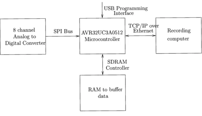
USB Programming
Interface
8 channel
Analog to
SPI Bus AVR32UC3AO512
Microcontroller
Recording computer
RAM to buffer data
Figure 2-1: Block diagram for NerdJack
The block diagram of the device meeting these functional requirements is given in Figure 2-1. The basic flow of information follows the marked arrows. The analog-to-digital converter is connected to the NILM system to be measured. This data is accepted by the microcontroller and buffered in external RAM. As the network becomes available, the data is streamed to a waiting personal computer or custom hardware for processing. The firmware on the microcontroller should be easily in-stalled using a USB cable for easy deployment.
2.1
Part selection
The aforementioned requirements led to fairly limited choices for the new device. The device needed to be a microcontroller-based single board computer system, so the first step was to pick the microcontroller. Ideal microcontrollers for this application would have peripherals to interface with external memory as well as communicate over Ethernet. This led to some of the high-end ARM processors and some of the Freescale ColdFire line of processors. Unfortunately, the devices that had both features tended
to have large pin counts in BGA packaging, making them unsuitable for this project. The final choice was the new Atmel AVR32 line of processors. These devices were in pre-release at the time, but they had the needed features in a flat package that could be soldered by hand. These chips could interface with external memory and had an Ethernet MAC module in addition to the standard microcontroller communication features. Best of all, the free GNU C Compiler Collection tools could be used for code development.
The next step was to select an analog-to-digital converter. The AVR32 microcon-troller has an on-board analog-to-digital converter, but it is of very limited resolution. This led to the selection of an external converter with a digital interface to the mi-crocontroller. This converter needed to be able to capture channels at 16 bits of accuracy, with either unipolar or bipolar inputs. The Analog Devices AD7656 was chosen because it could sample six channels on a single chip and communicate with a microcontroller using a standard SPI bus. A serial interface was important because the external data bus of the AVR32 used most of its input/output pins. A parallel interface would have used too many microcontroller pins. In addition, the AD7656 allows multiple AD7656 chips to be connected in a daisy-chain configuration. With this selection two chips would provide twelve channels of sampling using only one SPI port on the microcontroller. This solution would still give the needed sampling rate because the SPI bus can operate at a high clock speed.
2.2
Software selection
The device firmware must manage a variety of different tasks, including operating the network, communicating with the analog-to-digital converters, and buffering the data into SDRAM. This led to the selection of a real time operating system and a networking stack.
After examining a few of the operating systems already ported to AVR32,
FreeR-TOS version 5.0.4 was the best match for the device requirements. It is free, lightweight,
paral-lel prioritized tasks. Much like a full-featured operating system, it ensures that the highest priority ready task is running at all times. It also manages primitives like mailboxes and semaphores to allow inter-task communication and cooperation.
The other major library selection is lwIP, the Lightweight Internet Protocol stack version 1.3.0. This library provides a simple abstraction to the Ethernet interface using TCP/IP, the standard protocol of the Internet. It implements enough of the TCP/IP protocol to interface with standard network hardware without requiring too much processor overhead.
2.3
Hardware development
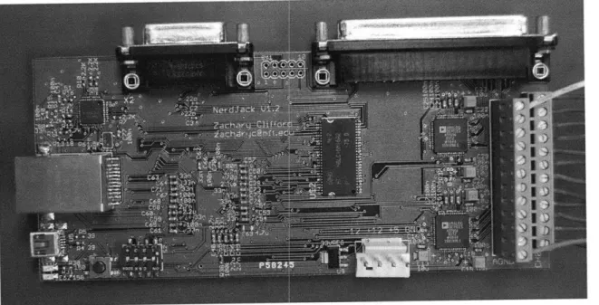
The EVK1100 evaluation kit from Atmel was used as a starting point for the design. This small board interfaced SDRAM and Ethernet to the microcontroller as well as many other peripherals. The AD7656 was then connected to this core module to begin testing and software development. The final design used the basic EVK1100 schematic with unnecessary peripherals removed and analog-to-digital converters added. The design was then rerouted on a two layer board with the same pin-out interface as the LabJack.
CadSoft's EAGLE layout editor was used to create the custom printed circuit board using the EVK1100 bill of materials and provided schematic as a starting point. Careful attention to the power supply decoupling and analog front-end were required for proper functionality. Additionally, many of the data and address lines from the SDRAM had to be properly separated from the clock signals on the board. The final board is pictured in Figures 2-2 and 2-3, while the final schematics are included in Appendix C. The analog-to-digital converters are connected to both the screwtab terminals and the DB connectors along the top edge. The Ethernet and USB connections for data acquisition and firmware programming respectively lie opposite to the screwtab terminals. The DIP switches set network parameters for the device, and the LEDs report its status. The device has power regulators that accept bipolar
delivered to the DB connectors to help expand the device. The DB connectors also hold some digital input/output pins and a UART serial port.
Figure 2-2: Top surface of data acquisition device
2.4
Device-side application
2.4.1
Overview
Most of the complexity of the device is in its onboard firmware. The microcontroller is programmed via USB with custom firmware once the device is built. The firmware application on the device is organized into a collection of interacting tasks that coor-dinate the sampling and transmission of data from the analog-to-digital converters.
All of these tasks are coordinated by FreeRTOS. Each one is a non-terminating
rou-tine with a private stack and priority level from zero to seven. Tasks can ready each other or be readied by interrupt service routines tied to external events. FreeRTOS
ensures the the highest priority ready task is executing. If multiple tasks of the same priority are ready, it switches between them in a round-robin style.
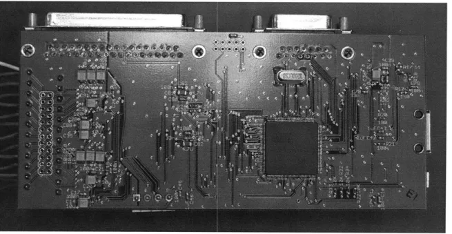
Figure 2-3: Bottom surface of data acquisition device
AVR32. The basic web server demo served as a baseline for development. The firmware has the same basic structure as the framework, but a new version of
FreeR-TOS version 5.0.4 was added, and numerous changes were made to the driver level
to fix bugs and add needed features. The framework drivers and operating system configure the resources of the device and provide an API for interacting with it. After setup, the framework hands control of the device to the application.
After powering the device on, the application initializes the hardware resources needed for interacting with the ADCs and the Ethernet module and waits for sampling commands from the PC host. A sampling command tells the device which channels to sample, the sampling rate, and the range required. This allows the device to trade dynamic range for accuracy if desired. Sampling continues until the PC requests a sampling stop or the device depletes its buffer space. Data is delivered to the PC in real-time, so buffering is only necessary in the event of network congestion. Software mechanisms are in place to resume interrupted transfers without losing samples using both the network stack and the features of FreeRTOS.
2.4.2
Interrupts
The scheme for sampling the analog-to-digital converters is a complex interaction of a few different interrupt service routines. The analog-to-digital converters are connected to a pulse width modulation generator on the AVR32. This is set to produce a sampling pulse at the chosen sampling frequency. Because of the daisy-chain nature of the ADCs, all channels less than the highest desired channel must be sampled. This sampling pulse causes a BUSY line to become active on the ADCs for the duration of the sampling. When this line falls, it signals an interrupt handler on the AVR32 that data is ready for reading.
This interrupt handler loads one of the Direct Memory Access (DMA) modules of the microcontroller. This module simply requires a source peripheral, a destination memory address, and the number of bytes to copy. Without CPU interaction it will copy this information and can use an interrupt to signal completion. The DMA module in this case transfers dummy data to the ADCs. Because of the nature of an SPI bus, the "slave" (the ADC) cannot initiate a transfer. When the "master" writes data to the slave, the slave will simultaneously send data back to the master. Therefore, the master must write dummy data to the slave to read its data. This DMA module performs this task every time the ADCs indicate that they have data ready through the BUSY line. This handler is of the highest supported priority because it is imperative that reading data begin as soon as data is ready. If there is delay, the data might not be read before the next sampling pulse arrives. In that event, the remaining unread data would be lost. Any unpredictability in microcontroller response time would limit the speed of the device.
There is another interrupt handler tied to a different DMA module that reads in-formation from the ADCs. The aforementioned module writes data to the ADCs. This one reads large amounts of data from the ADCs into onboard SRAM in the AVR32. When it completes a full packet, this interrupt handler reloads the DMA module and signals the application that a packet is ready. Other tasks in the application then copy the packet into external SDRAM for buffering and eventual transmission.
Task Name Priority WDTtask 7 TCP/IP 6 Ethernet 6 samplemanager 5 copytask 4 DSTRM 3 CMD 2 AUTOD 1 Serial 1
Table 2.1: Priority levels for NerdJack
The interrupt service routines are very fast and cannot tightly interact with other parts of the application. For the second DMA interrupt a custom semaphore imple-mentation was required for speed. Invoking the FreeRTOS semaphore abstraction led to very slow preemptive task switching. The "light" semaphore implementation in-volves a shared global variable between an application task and the interrupt service routine. Interrupts are disabled before accessing the variable to guard against race conditions.
2.4.3
Task Overview
FreeRTOS manages a collection of tasks that cooperate to implement the application. The task priority levels are numbered 0 through 7 with higher numbers having higher priority. The tasks in priority order are given in Table 2.1. Each one has a private stack and a specific purpose in the application. An overview of the various cooperating tasks should clarify application operation.
2.4.4
WDTtask
The WDTtask manages the hardware Watchdog timer (WDT). The watchdog in the AVR32 is a simple timer that will reset the microcontroller if the timer is allowed to
expire. This serves as a failsafe that should reset the device in the event of a software failure without requiring manual power cycling. At regular intervals the other tasks
in the application send messages to check in with the watchdog task. The watchdog task resets the hardware watchdog timer when all other threads it monitors have checked in. Should all threads not check in for the allotted time, the hardware timer will reset the device.
2.4.5
TCP/IP and Ethernet
These are necessary for proper functioning of the Ethernet interface and iwIP TCP/IP stack. The Ethernet monitoring task simply waits to be readied by an interrupt tied to the Ethernet peripheral "receive" event. It then reads the incoming packet and passes it upwards to the lwIP stack. The TCP/IP task is responsible for sending and receiving TCP/IP packets on the Ethernet interface. It handles retransmission of lost packets and all necessary memory management. When the application calls an lwIP
API function, this routine takes over the processing of that request.
2.4.6
Samplemanager
This coordinates sampling of the ADC channels. When lower levels of the application wish to start sampling with certain parameters or stop it, a message is sent to this task. This ensures that race conditions do not develop with multiple parts of the application trying to alter the ADC parameters simultaneously. Because this task is the only one able to alter the converters, its internal state variables actually reflect the sampling parameters. This was necessary because sampling could be altered by both user requests and network failure. A single interface was required to prevent race conditions between those two command sources.
2.4.7
Copytask
Copytask was necessary to solve latency problems with external memory. The ap-plication is supposed to sample data into external SDRAM and then transmit it to a waiting PC for analysis. Most of this copying from the ADCs is performed using on-chip DMA hardware described above. The copying task was necessary because
the on-chip DMA hardware has no buffer and data is sampled simultaneously. This means that all channels of the ADC hardware become ready in bursts, but the DMA hardware is not designed for burst operation. If multiple channels are selected, a new 16-bit word of data arrives every 16 clock cycles. The SDRAM latency is long because it is engineered for burst operation, but it becomes unpredictable when the Ethernet task is taken into account. In the worst case scenario the TCP/IP stack is actively reading past data from the SDRAM while the DMA controller is trying to write a burst of data into a different part of SDRAM. The lack of any sort of buffering in the DMA hardware leads to data loss as these two modules contend for access to the SDRAM. This problem was solved by using on-chip SRAM as a buffer for the DMA hardware. The copy task is responsible for moving data from this internal buffer into external SDRAM. Although this scheme requires more total data movement, this re-lieves congestion because this copying can take place between data bursts from the
ADC hardware without tight real-time constraints.
2.4.8
DSTRM, CMD, and AUTOD
These three tasks are the network ones that listen on three different ports. The Command task listens on TCP and accepts single commands to start, stop, and resume sampling before closing the connection. The Autodetection task listens on a
UDP port and simply replies to datagrams sent on that port. This allows a PC to
use UDP broadcasts to detect the IP address of the device. It can look for replies and then use the source address of the reply to make this determination. The final task is the Datastream task. It waits for a TCP connection and then sends data through that connection as data becomes available.
2.4.9
Serial
Serial uses the USART serial port on the device. This task listens on the standard Telnet port and simply echoes characters received on that port to the serial port.
buffer space keeps the device running smoothly. This was added to make interfacing the system to other digital devices more straightforward.
The lowest priority task is the FreeRTOS Idle task. It performs required mainte-nance routines for the operating system kernel, but it is otherwise not important to the functioning of the application.
2.5
PC side application
Utility software for programming the device and reading data from it were devel-oped to interface with the device. Both of these were develdevel-oped in parallel with the hardware to make a full system ready for deployment outside of the laboratory. The device programmer is a mixture of C and Python, while the data reading program is purely C. Both were written to be as portable as possible between different PC operating systems and potentially other embedded systems.
The programming software utilizes fully open source software to perform this task. The device is equipped with a mini-USB port that allows it to be programmed using commodity USB cables. AVR32 devices are shipped pre-loaded with a bootloader that permits in system programming via USB. When the right conditions are met (in this case a switch on the device is flipped at bootup), the application is not loaded. Instead, the USB port is activated and ready to communicate using an Atmel variant of the USB Device Firmware Update protocol. Part of this project involved contributions to an open-source C utility called "dfu-programmer" to help implement this protocol in a cross-platform way. Extending the existing programming utility was much more straightforward that starting over. This utility is better than the Atmel-provided batchisp program because it can run on Windows, Macintosh, and other Unix derivatives like Linux. At its core it uses an open source program called libUSB. This library permits communication with the PC USB port with a very simple interface that is portable between different operating systems. Because of this dependence, dfu-programmer can operate on any system that provides a libusb-like interface. This utility takes as input AVR32 firmware and burns it to the AVR32.
It can also read the firmware image and interpret the settings programmed into the device.
Around this utility is a simple Python command line package called "nerdconfig". This package exposes a command-line interface to dfu-programmer that makes pro-gramming simple for the end-user. This utility burns stock firmware onto the device and programs it with a unique Ethernet address and serial number. Finally, it con-figures the IP address the device will assume after initialization. It can determine the firmware version running on the device and upgrade if necessary.
The serial number, MAC address, and IP settings are recorded to a special section of memory in the device known as the "User Page". The User Page is a section of Flash 512 bytes in size that is not erased by the Flash Erase command on the AVR32. This makes it suitable for configuration and serial number data.
The other PC software component is "ethstream". This command line program is a modification of an earlier "ljstream" written by Jim Paris for interfacing with the LabJack. Ethstream interfaces with both devices so that both old and new NILM hardware will work with the same PC-side software. This program accepts as input the channels to sample and the rate requested. It then outputs space separated samples to STDOUT. This allows the output to be easily piped to other programs for processing or redirected to a file for storage. It has other modes for testing the device, detecting its IP address, and determining its firmware revision. This software can also operate on Windows, Macintosh, and other Unix derivatives like Linux.
A manual for the entire system was written and is attached as Appendix B. This
details the usage and construction of the device. The source code to both PC-side applications and the device firmware is attached as Appendix F.
2.6
Testing and Results
2.6.1
Methods
Testing was an important part of the development process that helped ensure that the device met specifications.
The intended use of the device places it in a difficult place to physically access. Software crashes might not be noticed for some time, and manually resetting the device might not be possible. The device needed to be able to successfully start acquisition every time it was asked to do so. In any normal failure condition it needed to reset without human intervention.
To evaluate it a test fixture was created that started ten thousand acquisitions with random sampling parameters. The device was connected to a resistor ladder to assert known voltages on each channel. Easy automated tests programmatically confirmed that the proper channels were being sampled for the correct amount of time.
Another test involved running the device for a full day with a sine wave on one channel and the resistor ladder on the others. The sine wave was programmatically tested to ensure that points were not lost or mixed up in any way with the known voltages asserted by the resistor ladder.
The device sampled at a variety of speeds under different network conditions to evaluate its actual sampling rate limitations.
The final test involved using a Matlab code called ADCTest to evaluate the ac-curacy of the device. This code takes a few periods of a perfect sine wave captured
by the device and analyzes it. It computes the effective bit accuracy of the device by
measuring how closely it follows the reference sine wave.
2.6.2
Results
The device passed both functional tests with the latest revision of firmware by starting every time in capturing the correct data. It did not crash or mix up channels in
multiple 24 hour tests. It also kept accurate time during that period.
The effective accuracy of the device appears to be 11 bits according to the
previ-ously mentioned Matlab package, but there is reason to believe that it is better than that. A Wavetek Function Generator Model 182A calibrated on 8/21/92 generated the reference sine wave. It is unclear whether the observed bit rate is limited by the resolution of the sensing device or the signal generator. The apparent accuracy changes with the amplitude and frequency of the sine wave. However, the measured accuracy in this test was superior to the LabJack used as a reference. Because the board was designed to the specifications of the ADC manufacturer, it should match
the performance specified by Analog Devices. A new signal generator was not pur-chased for testing because the new device is already demonstrably better than the reference device. The new device passes this test.
The sampling rate of the device is constrained by the SPI bus of the microcon-troller connection to the analog-to-digital converters. The network had to be highly congested for it to become a performance bottleneck. As such, the sampling speed is
determined by how much data needs to be copied from the analog-to-digital convert-ers. Data is read out from the converters serially starting with channel zero. Since each 16 bit sample requires sixteen more periods of the 18 MHz SPI clock, every chan-nel sampled increases the amount of time required to empty the converter of data. There is no mechanism for sampling high numbered channels without first reading out lower channels, so the constraint applies to the highest channel sampled. These limitations are built in to the PC client to NerdJack to provide warnings to the user about potential data corruption. These tests showed that the NerdJack could sample
Chapter 3
Inductively powered current sensor
3.1
Introduction and Motivation
For NILM to be deployable in wider settings, it would need to be installed without the help of a trained electrician, and it would need to attach to standard equipment. Elec-trical current is difficult to probe because any sensor needs to be located "upstream" of any loads to be measured. Directly measuring the incoming utility connection is difficult because the connection is inaccessible or at least non-standard among homes or other systems. Additionally, utility connection bundles usually consist of both the power and return path connections. This makes inductively measuring the current difficult because the net current flowing in the bundle is zero in the absence of energy storage in the home or ground faults.
A small sensor described in this chapter placed inside a standard circuit breaker
panel allows for this measurement. This configuration is advantageous because a circuit breaker panel and circuit breaker are both very standard devices that are all constructed similarly. Each breaker also carries line current without the neutral connection nearby. The sensor consists of two parts both magnetically attached to the steel door of the breaker panel hereafter referred to as the "inner" component and the "outer" component. The inner component rests up against the main breaker in the circuit breaker box to inductively sense the current flowing in the breaker. This device then modulates the sensed waveform onto a carrier waveform via a novel
low-power JFET mixer. This data is then transmitted through the door to be received by the external part of the sensor. The outer component inductively powers the internal device and receives signal from it. All of this is accomplished without drilling any holes in the steel door.
3.2
System Overview
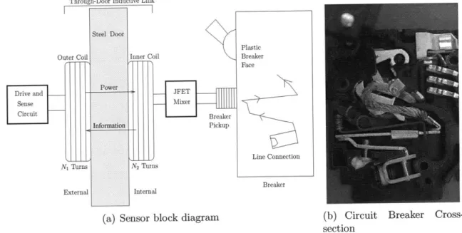
The sensor shown in Figure 3-1 (a) consists of three main parts: an inductive pickup for sensing current from the breaker face (Breaker Pickup), an inductive link designed to transmit power through the steel breaker panel door (Through-door Inductive Link), and a balanced JFET modulator circuit for transmitting information through that inductive link (JFET Mixer).
Through-Door Inductive Link
Steel Door
Plastic
Outer Coil Inner Coil Breaker
Drive and _oe _H _ JET
Sense
___lMixer~-Circuit Breaker
Information __Pickup
s -s -_ _ aLine Connection
N1 Turns N2 Turns
External Internal Breaker
(a) Sensor block diagram (b) Circuit Breaker
Cross-section
Figure 3-1: The current sensor measures magnetic fields at the face of the circuit breaker and modulates a high frequency carrier signal to transmit that information through the panel door.
The outer coil in Figure 3-1(a) is driven with a high-frequency sinusoidal carrier voltage. That voltage couples to the inner coil through the inductive link in Figure 3-1(a) and drives the JFET mixer. The JFET mixer controls the amount of current drawn from the inner coil according to the low-frequency (60 Hz) current signal
mea-sured by the breaker pickup. The result is a modulation between the high frequency carrier signal and the low-frequency (60 Hz) signal measured at the breaker face. The external sense circuit in Figure 3-1(a) monitors the current drawn through the inductive link to extract the resulting modulated signal. The internal device is fully powered by the applied carrier, and the entire system works without modification to the breaker panel or the circuit breaker itself. With the modulated signal available to the sense circuit external to the door, the current through the main breaker can be analyzed with the NILM system described above for load identification and power monitoring [13, 3, 5, 7, 11, 6, 14, 9, 10, 2, 12]. The sense circuit consists of both a
power supply stage to drive the coils and an I/Q demodulation stage to recover the measured current.
3.3
Breaker Pickup
The current path inside a typical circuit breaker passes by the lower face of the circuit breaker as illustrated by Figures 3-1(a) and 3-1(b). Therefore the breaker pickup was
designed to focus and measure the magnetic field resulting from current flowing inside the lower breaker face.
f f
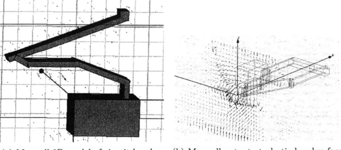
(a) Maxwell 3D model of circuit breaker (b) Maxwell output at plastic breaker face
Figure 3-2: Maxwell 3D model of breaker with field lines drawn at the breaker face. One figure is from above and the other is angled to show field lines. The extra bar at the back of the view was added to complete the current path and has no effect on the field shown.
Ansoft's Maxwell 3D was used to model the current carrying member to identify the appropriate location of the breaker pickup. The output from this software is shown in Figures 3-2(a) and 3-2(b). The plane of magnetic field vectors is the plane of the plastic breaker face. The predominant flow of current through the circuit breaker is from top to bottom, so the magnetic fields were expected to wrap around the current carrying member across the breaker face. Rom Figure 3-1(b), this corresponds to a flux into the page just to the left of the breaker. Maxwell 3D confirmed that this was the appropriate model of the breaker and that the best position for the pickup was on top of the breaker where the metal is closest to the breaker face. At that point the magnetic field is most uniform and strongest.
The free software FEMM (Finite Element Method Magnetics) in its two dimen-sional mode was used to design the pickup. This software was written by David Meeker and can be downloaded from http: //www. f emm. inf o/wiki/HomePage. It can model the fields generated by sources into and out of a two dimensional plane. The Maxwell 3D model showed that the field at the surface strongly resembles the field produced by a point current source at the depth of the current carrying member. In FEMM, the plastic breaker face was modeled as air, and an analysis of the ge-ometry was conducted. Various pickup shapes were considered to yield the strongest concentration of magnetic flux in the pickup core. An ideal pickup would focus as much magnetic flux into itself as possible, so it needed to roughly follow the magnetic field. FEMM showed that a half toroid of high permeability material placed on the breaker face was suitable in that it would result in significant flux-focusing in the material. The output of this program is shown in Figure 3-3. This is a representation of the breaker and pickup down its long axis.
This flux needed to be efficiently converted to an electrical signal. One possibility involved a Hall Effect sensor. This was not ideal because such a sensor would require voltage rails on the inside of the door where power is highly constrained. A coil was chosen for the sensor because the magnetic flux would directly produce a voltage signal that could be immediately used in the circuit.
Figure 3-3: Finite Element Magnetic Model (FEMM) of magnetic flux through the breaker. The plastic breaker is ignored because it is not conductive or permeable to the magnetic flux.
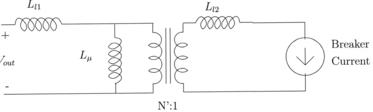
L
1,
L
12
Breaker Current
N':1
Figure 3-4: Breaker pickup model. The breaker pickup looks like a virtual transformer around the current to be measured.
is a 1:N' step up transformer with poor coupling shown in Figure 3-4 where N' < N
may be used to model the poor coupling from the breaker current member to the N turn windings. The current source inside the breaker face is modeled as driving the single turn of a 1:N' turn virtual transformer. The leakage inductances L11 and L12
of the transformer are expected to be large because a large portion of f the magnetic path consists of air instead of high [t material.
Looking at the model in Figure 3-4, the breaker pickup is nonlinear across fre-quency. NILM is interested in harmonics of 60 Hz. The breaker pickup is connected to stages that measure open circuit voltage and do not load it very much. This means, according to the proposed model in Figure 3-4, that the output is approximately the voltage that the current source generates across the magnetizing inductance L, given in Equation (3.1). In Equation (3.1), L, is the magnetizing inductance, L12 is the
sec-ondary leakage inductance, w is the breaker current frequency and 'in is the breaker
current magnitude.
V oc 27rjwL1IJi xt (3.1)
From this Equation it is clear that Vst is a function of both In and w. This nonlinearity applies gain to higher harmonics that must be characterized in the full system. It is clear that a higher L, will lead to higher output voltage. From the Equation it is also clear that different frequencies will leave
The geometry of the coil fixes the level of leakage in this transformer. Using a high p material for the toroid and matching the shape of the toroid to the natural magnetic field lines make N' approach the true N. Increasing the cross sectional area of the toroid increases the flux it can capture and thereby improves coupling in the same manner.
Turns on the pickup are related to the turns ratio of the virtual transformer and the inductance looking into the pickup coil. The coupling is fixed by the geometry of the pickup and breaker. The easiest way to increase magnetizing inductance is to simply add more turns. Having a high magnetizing inductance is critical to proper
functioning of the circuit, otherwise, it tends to short out the signal to be measured. Unfortunately, the desired 60 Hz signal needs a high inductance for the impedance at that frequency to become appreciable i.e., Z, = wL,1 will be small when w = 27r *60.
Wire selection for the pickup was simplified by later stages of the JFET Mixer. At 60 Hz skin effect is negligible, and the pickup is not significantly loaded. This means that a very fine wire gauge can be used because its series resistance will not impact a voltage measurement of the coil.
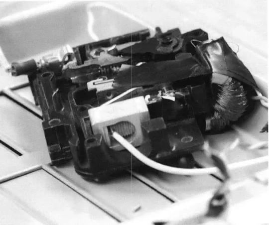
Using the proposed virtual transformer model in Figure 3-4 as a design guide, a Ferroxcube part TX25/15/10-3E6 was used with 1200 turns of 34 AWG magnet wire. The toroid has a 25 mm outer diameter, a 15 mm inner diameter, and a 10 mm thickness. This toroid was cut in half on a diamond band saw, and the two halves were glued together side by side to increase cross sectional area. This toroid has a very high relative permeability of approximately 10000to [4]. A photograph of this toroid affixed to the breaker is shown as Figure 3-5. The exposed current carrying member is partially obscured by electrical tape, but the wound toroid is clearly visible.
The voltage signal from this pickup still is too small to drive the JFET mixer
at small current signal levels. A 1:14.1 step-up audio transformer module was added between the JFET mixer and the pickup. The audio transformer works at low frequen-cies and has enough turns that its own magnetizing inductance does not significantly load down the pickup coils at 60 Hz.
An additional resonant capacitor could be added to the audio step up transformer to boost signal levels at the cost of distortion. Normally, resonating with a small inductor at low frequency would require a large capacitor. In this case the inductor is reflected across the transformer, increasing its apparent impedance by the square of the turns ratio. This allows for a more reasonable choice of capacitor when added to the transformer secondary. The capacitor would need to be the appropriate value to resonate with the parallel combination of the magnetizing inductance of the au-dio transformer and the reflected inductance of the pickup. This method provides more voltage gain at the desired 60 Hz signal frequency while attenuating the higher harmonics that are important to NILM function and introducing a 180 degree phase
shift. This was not used in the experimental setup because gain was sufficient without it. In experiments two .47 pF capacitors were placed in parallel with the secondary of the transformer, but they were removed as they became unnecessary.
3.4
JFET Mixer
The four-quadrant balanced JFET modulator (mixer), shown in Figure 3-6, was de-signed to transmit information from the breaker pickup through the inductive link and out of the breaker panel. This circuit consists of two JFET devices for modula-tion control and two resistors to improve linearity, but it does not require a DC power
supply.
Imod
SR 1 VSg
Vcarrier I>
R2 -+
Figure 3-6: Adaptive Referencing Balanced two-JFET Modulator circuit enables si-multaneous powering and modulation with no DC bus required
The JFET mixer can be modeled as a time-varying load on the carrier voltage source, Varrier in Figure 3-6. In the circuit breaker system of Figure 3-1(a) the carrier voltage source that drives the JFET mixer is the voltage on the inner coil which couples from the outer coil. The load presented to Vcarrier in Figure 3-6 varies with the control signal Vig applied to the JFET gates and leads to a corresponding modulation of the current Imod. The two-JFET mixer circuit is particularly advantageous for this application because it requires a minimal amount of circuitry inside the breaker door and lends itself to a low-cost solution.
normally-on device that requires a negative gate to source voltage V, to turn it off. It is a symmetric device, meaning that the drain and source are interchangeable. By convention the source is the side of the JFET at a lower potential than the drain.
This circuit is best examined in half cycles of the carrier supply. On positive half cycles the lower JFET is fully turned on because the from the breaker pickup, Vig signal drives its V, positive making its gate voltage much higher than both its drain and source. This JFET becomes a small on state resistance. Since the currents are
low, the two resistors shown in Figure 3-6 drop little voltage. Most of the carrier
voltage is impressed across the top JFET device. The top JFET then has a negative voltage applied to its gate due to Vig that causes its current to be controlled by Vig.
Vig from the breaker pickup is a bipolar signal, but this is controlled because the
circuit is self-referencing. The voltage drop across the top resistor R acts to bias Vj9
because Vg, is equal to Vi, - VR with VR the drop across the top resistor. As long as R is large enough, VR will always be less than Viq to keep the JFET device controlled. Approximating V, of the JFET as constant, the current through it then reduces to
vn - V-igVg
R R
On negative half-cycles of the carrier supply, the situation is reversed. In this way the symmetric nature of the JFET stack permits control during both half cycles of the applied sinusoid. Square wave multiplication of the two input signals is achieved because the sign of the mixer current matches the sign of the carrier while the am-plitude is determined by the breaker pickup. This causes the envelope of the carrier to track the breaker pickup signal, yielding simple amplitude modulation. Because there is always some steady current in the system, the carrier is not suppressed. The signal looks like Equation (3.2) with we the carrier frequency, A the remaining carrier amplitude, and M the modulation amplitude. Some higher frequency terms appear after simplification of this expression, but with appropriate demodulation, the higher harmonics can be filtered away.
The two resistors have been inserted to improve the performance of the mixer. They limit the steady state current of the mixer and improve the linearity of the response to the control voltage. This comes at the cost of gain, so an optimum choice balances those two concerns.
A small signal analysis of the circuit details its gain and design strategy. The
symmetry of the device means that an examination of the circuit during one half cycle can be applied to its operation on the other one. In this analysis it is assumed that the voltage applied is well above the saturation voltage of the JFET devices and that it makes quick zero crossings. Ideally, the applied source should be a square wave, but a large enough sine wave is sufficient for proper operation.
Assuming a valid steady state voltage VdS is impressed over the JFET and the Vg, is higher than its pinch-off voltage V, it will admit a current Id. These are set by the
JFET parameters, the two resistors, and the source impedance of the carrier supply.
In a small signal sense, the top JFET device looks like a resistor r, in parallel with a current source with magnitude gmVgs. The transconductance gm is given in Equation
(3.3) in terms of JFET parameters
#
and Id. with#
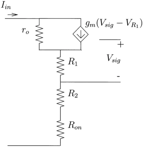
a JFET gain parameter. The output resistance r, as in Figure 3-7 is !+1/A with A the channel length modulation parameter of the JFET. The bottom JFET device looks like a small Ron resistor. Ron is assumed to be small compared to R1 and R2.gmn = (3.3)
Under the assumption that the sum of R1, R2, and Ron is much smaller than ro,
simple expressions for the gain of the circuit can be found. The top JFET device is modeled as a transconductance source in parallel with a resistor ro as shown in Figure
3-7. Looking at the small signal model in Figure 3-7, the transconductance source
of the top JFET device has a value of gmVs = gm(Vig - VRi). VRi is simply the current delivered through the current source, Iin if current through ro is negligible. Rearranging terms to solve for i-, the gain G of the circuit, yields the gain from
s ig
'in
ro
gm(Vsig
VR1)
Vsig
Figure 3-7: Small signal model for JFET Mixer
maximized within the power constraints of the door and the linearity provided by having a bigger R1.
G = 9" (3.4)
1 + gmR 1
With this small signal understanding of the JFET mixer, actual JFET devices can be selected. The two most important device parameters are the
3
and the V, of the device. Bigger#
increases gn. It also increases the zero input Id because theJFET gate is further away from pinchoff. V is negative in JFET devices. However,
bigger V values require larger V, values to maintain saturation. Operating under the assumption that gm * R1 << 1 means that the gain is proportional to gm. With some