Publisher’s version / Version de l'éditeur:
Journal of the American Chemical Society, 139, 22, pp. 7436-7439, 2017-05-29
READ THESE TERMS AND CONDITIONS CAREFULLY BEFORE USING THIS WEBSITE.
https://nrc-publications.canada.ca/eng/copyright
Vous avez des questions? Nous pouvons vous aider. Pour communiquer directement avec un auteur, consultez la
première page de la revue dans laquelle son article a été publié afin de trouver ses coordonnées. Si vous n’arrivez pas à les repérer, communiquez avec nous à [email protected].
Questions? Contact the NRC Publications Archive team at
[email protected]. If you wish to email the authors directly, please see the first page of the publication for their contact information.
NRC Publications Archive
Archives des publications du CNRC
This publication could be one of several versions: author’s original, accepted manuscript or the publisher’s version. / La version de cette publication peut être l’une des suivantes : la version prépublication de l’auteur, la version acceptée du manuscrit ou la version de l’éditeur.
For the publisher’s version, please access the DOI link below./ Pour consulter la version de l’éditeur, utilisez le lien DOI ci-dessous.
https://doi.org/10.1021/jacs.7b02563
Access and use of this website and the material on it are subject to the Terms and Conditions set forth at
Robust bipolar light emission and charge transport in symmetric
molecular junctions
Tefashe, Ushula M.; Nguyen, Quyen Van; Lafolet, Frederic; Lacroix,
Jean-Christophe; Mccreery, Richard L.
https://publications-cnrc.canada.ca/fra/droits
L’accès à ce site Web et l’utilisation de son contenu sont assujettis aux conditions présentées dans le site LISEZ CES CONDITIONS ATTENTIVEMENT AVANT D’UTILISER CE SITE WEB.
NRC Publications Record / Notice d'Archives des publications de CNRC:
https://nrc-publications.canada.ca/eng/view/object/?id=9369903f-862f-49e8-9756-d13ea510c17d https://publications-cnrc.canada.ca/fra/voir/objet/?id=9369903f-862f-49e8-9756-d13ea510c17d
Robust Bipolar Light Emission and Charge Transport in Symmetric
Molecular Junctions
Ushula M. Tefashe,
†Quyen Van Nguyen,
‡Frederic Lafolet,
‡Jean-Christophe Lacroix,
*
,‡and Richard L. McCreery
*
,†,§†
Department of Chemistry, University of Alberta, 11421 Saskatchewan Drive, Edmonton, Alberta T6G 2M9, Canada
‡
Université Paris Diderot, Sorbonne Paris Cité, ITODYS, UMR 7086 CNRS, 15 rue Jean-Antoine de Baïf, 75205 Paris Cedex 13, France
§
National Institute for Nanotechnology, 11421 Saskatchewan Drive, Edmonton, Alberta T6G 2M9, Canada
*
S Supporting InformationABSTRACT: Molecular junctions consisting of a Ru-(bpy)3 oligomer between conducting carbon contacts
exhibit an exponential dependence of junction current on molecular layer thickness (d) similar to that observed for other aromatic devices when d < 4 nm. However, when d > 4 nm, a change in transport mechanism occurs which coincides with light emission in the range of 600−900 nm. Unlike light emission from electrochemical cells or solid-state films containing Ru(bpy)3, emission is bipolar, occurs
in vacuum, has rapid rise time (<5 ms), and persists for >10 h. Light emission directly indicates simultaneous hole and electron injection and transport, possibly resonant due to the high electric field present (>3 MV/cm). Transport differs fundamentally from previous tunneling and hopping mechanisms and is a clear “molecular signature” relating molecular structure to electronic behavior.
A
primary objective of the field of molecular electronics is to control electronic behavior by varying the structures of molecular layers between conducting contacts in order to realize electronic functions not possible with silicon. Realization of this goal will require understanding charge transport in very thin molecular layers (<1 to 25 nm), in particular how orbital energies, hybridization, and electronic coupling to the contacts control electron transport. We describe here a molecular junction (MJ) containing a molecular layer of a ruthenium bipyridyl derivative with transport distances (d) of 1.6−12.8 nm between conducting carbon contacts. Not only do such junctions demonstrate a clear change in transport mechanism for d > 4 nm, but they also emit visible light when the applied bias (V) exceeds ∼2.7 V. The change in mechanism and onset of light emission coincide and indicate a distinct charge transport mode when V > 2.7 V and d > 4 nm. The new mechanism is consistent with bipolar injection of carriers into the highest occupied and and lowest unoccupied molecular orbitals (HOMO and LUMO) of the Ru(bpy)3 centersfollowed by recombination and light emission, and it differs fundamentally from previously reported light emission via electrogenerated chemiluminescence1−3 or in light-emitting
diodes.4−6
Molecular junctions were fabricated by established meth-ods,7,8 all with the same Au30/eC10/ Ru(bpy)3P/eC10/Au20
structure, where “eC” is electron-beam deposited carbon9,10 and subscripts indicate layer thicknesses in nm. “Ru(bpy)3P”
represents a molecular multilayer with the structure shown in
Figure 1A, which was deposited from a phenyl-diazonium
derivative of Ru(bpy)3(PF6)2 as described in the Supporting Information(SI, sections 1 and 2). The resulting MJ structure shown inFigure 1B was made with high yield by deposition of an eC/Au top contact, and the Ru(bpy)3P layer thickness
varied from 1.6 ± 0.3 to 12.8 ± 0.7 nm, as confirmed by atomic force microscopy “scratching”11 as shown in Figure S2. Characterization by Raman and X-ray photoelectron spectros-copy of the Ru(bpy)3P thin films (SIsections 4 and 5) indicates
that the Ru(bpy)3P centers are not modified significantly
during film formation and the P:Ru atomic ratio is 2.1, close to the expected 2.0.
The current-density vs bias (J−V) curves for Ru(bpy)3P MJs
shown inFigure 2A are symmetric with respect to polarity and show a strong dependence on thickness, similar to other aromatic MJs reported previously.12−14 The J−V response is
independent of scan rate in a vacuum (Figure S7) and is stable for thousands of cycles.Figure 2B compares the J−V response
Received: March 21, 2017 Published: May 20, 2017
Figure 1.(A) Structure of the Ru(bpy)3P molecular layer deposited
on eC substrate. (B) Schematic illustration of Cr4/Au30/eC10/
Ru(bpy)3P/eC10/Au20molecular junction.
to those of identical junctions made with nitroazobenzene (NAB) instead of Ru(bpy)3P, with both obtained in a vacuum
(<10−5Torr) at a scan rate of 1000 V/s. For d = 3.2 nm, the J−
V curves are nearly identical, with a small difference shown in
the inset of Figure 2B. This similarity is consistent with previously reported results on aromatic MJs, in which seven different molecules with >2 eV range of HOMO and LUMO energies had statistically identical current densities when d < 5 nm.15However, for thicker devices with d = 12.8 nm, the J−V responses differ greatly, with J for Ru(bpy)3P larger than J for
NAB, by a factor of >30 at V = 2.5 V.Figure 2C shows plots of ln J vs d (i.e., “β plots”) for Ru(bpy)3P at several bias values, to
illustrate the dependence of current on layer thickness. At V = 0.2 or 0.5 V, there are two distinct slopes, with β = 2.4 nm−1at
d < 4 nm and β = 0.70 nm−1for d = 5−11 nm, which decreases
to 0.47 nm−1for V = 3 V.Figure 2D compares the β plots for
Ru(bpy)3P and NAB for V = 0.5 V. Changes in the slopes of β
plots have been attributed to transitions between conduction mechanisms, such as tunneling to activated “hopping”16−18or
field ionization.14As discussed next, the underlying mechanism in Ru(bpy)3P causing the change in β can be elucidated using
light emission.
Light emission by Ru(bpy)3derivatives has been reported for
decades, in electrochemiluminescence,19,20 light-emitting elec-trochemical cells,1,6and light-emitting diodes.2,5,21Figure 3A,B shows light emission from a Ru(bpy)3P MJ with d = 12.8 nm
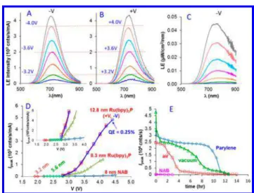
for positive and negative bias. The sign on the bias is the bottom contact (30 nm Au) relative to the top (20 nm Au), and light was always observed through the top contact. Light emission spectra for Ru(bpy)3P devices with d = 12.8 nm,
collected with a spectrograph/CCD system described pre-viously,8,12are shown inFigure 3A for a bias range of −3.0 to −4.2 V. The intensities of each spectrum were normalized by the junction current to yield units of counts s−1mA−1.Figure 3B shows spectra from the same device but with reversed bias, which clearly indicate that emission is nearly identical for positive and negative bias, with no change in peak intensity or wavelength with bias polarity. In both cases, the efficiency of light emission in terms of light intensity per unit of junction current increases with bias, with a threshold for emission at
∼2.7 V. Correction of the negative bias spectrum for instrument response using a standard white light source as described previously12 yielded Figure 3C. Light emission spectra for four Ru(bpy)3P thicknesses are provided inFigure S5, and their peak intensities are plotted vs bias voltage in
Figure 3D. Note particularly that emission is very weak for d < 8 nm, and a clear threshold for emission occurs at V = 2.7 V. A similar threshold has been reported for light emission in asymmetric solid-state Ru(bpy)3 devices1,3−5,22 with >80 nm
layer thicknesses and likely quite distinct transport mechanisms (see below). Also, shown inFigure S6andFigure 3D are light emission from NAB with the same device structure, with Ru(bpy)3P emission >50 times that of NAB for d = 12.8 nm
and V = 4.2 V. Unlike Ru(bpy)3P, emission from NAB
junctions is polarity sensitive, with negative bias yielding approximately twice the light intensity of positive bias.8 We conclude that Ru(bpy)3P light emission is governed by a
distinct mechanism from the hot-electron model described previously,8,12due to the known luminescence of Ru(bpy)32+
complexes.
Light emission by electrochemical cells and solid-state devices with thicknesses >70 nm is meditated by generation of Ru3+ and Ru+ centers, followed by recombination to form
excited Ru(bpy)32+*, which emits light. Light emission from
solid-state Ru(bpy)3(PF6)2polymers shows strong dependence
on anion mobility and the presence of water or residual solvent, which were attributed to electrochemical generation of Ru3+
and Ru+at the electrode interfaces.2,3,5,6They exhibited strong
sensitivity to bias polarity and the electrode material, and a delay in light emission of several seconds which was strongly affected by the counterion identity.1 Handy et al.4 reported light emission from solid-state 70−100 nm films of Ru(bpy)3
derivatives between ITO and Al electrodes with onset delays of several minutes at 3 V bias and a few seconds at 5 V bias. The response time and effects of atmosphere on the current Ru(bpy)3P devices are shown inFigures 4 and 3E. The J−V
Figure 2.(A) J−V curves for Cr4/Au30/eC10/ Ru(bpy)3P/eC10/Au20
junctions (averages of 8 MJs, in vacuum) with thickness (d, nm) indicated for each curve. (B) J−V responses of NAB and Ru(bpy)3P
MJs with same device structure and thickness. (C) Attenuation plots for Ru(bpy)3P MJs for five bias values and slopes (β) indicated. (D)
Attenuation plots for Ru(bpy)3P and NAB devices for V = 0.5 V.
Figure 3. Light emission spectra from Ru(bpy)3P junctions for
negative (A) and positive (B) bias, with Vapp= ±3.0, 3.2, 3.4, 3.6, 3.8,
4.0, and 4.2 V. (C) Spectra of panel A after correction for instrument response. (D) Peak emission intensity normalized to junction current vs Vappfrom Ru(bpy)3P MJs with d = 3.2, 5.6, 8.3, and 12.8 nm (both
+V and −V bias) and a NAB junction (d = 8 nm). (E) Light emission vs time for a continuously applied bias of 2.8 V for Ru(bpy)3P junction
(d = 12.8 nm) in air, under a vacuum, and in air-protected Parylene. The weak NAB emission (pink) decreases from 200 to 0 counts s−1
after 3 h in air.
Journal of the American Chemical Society Communication
DOI:10.1021/jacs.7b02563 J. Am. Chem. Soc. 2017, 139, 7436−7439
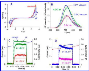
responses in vacuum were strongly affected by addition of either air or water vapor, developing the hysteresis shown in
Figure 4A. The J−V response in vacuum is independent of scan rate, but in air it shows significant variations with scan rate (see
Figure S7). The emission spectra exhibit lower intensity in air (Figure 4B) and a slight shift in peak wavelength. Small shifts in peak wavelength (<20 nm) with thickness, bias, and atmosphere (Figures 4B and S5) may be due to the effects of strong applied electric field, as discussed below. As shown in
Figure 4C, a bias pulse in vacuum produces a fast, nearly square current transient (rise time < 50 μs), with light emission lagging a few milliseconds for Vapp= 3.6 or 4.0 V. In air (Figure 4D) the
current rises over a period of ∼20 ms, and light emission decays with time. Additional pulse transients are provided inFigure S8. Finally, the stability of light emission is shown inFigure 3E for a continuous bias of 2.8 V. In air, emission decreases by ∼90% in 4 h, while in vacuum it lasts approximately twice as long.
Figure 3E also shows the emission of a Ru(bpy)3P MJ (d = 12.8
nm) protected by 500 nm of Parylene film deposited in vacuum (SI, section 10). After a brief decline, emission decreases slowly for >10 h before a rapid decline to near zero. The fast decline of intensity at short times (<20 min) is likely due to residual water in the devices.
For d < 4 nm, the transport mechanism of Ru(bpy)3P
junctions is likely similar to the quantum mechanical tunneling, possibly coherent, reported for many examples of conjugated or aromatic molecules. Electronic coupling between the carbon substrate and molecular layer reduces the effects of molecular structure on transport, as described previously for carbon-based MJs15 and for metal/organic interfaces.23,24 Light emission is weak for d < 5 nm and attributed to hot electrons traversing the molecular layer and emitting light in the top contact.8,12 For NAB, light emission increases gradually with bias, is asymmetric with polarity, and is not strongly dependent on layer thickness. However, when d > 4 nm, Ru(bpy)3P devices exhibit behaviors
very different from those of NAB in both the magnitude and attenuation of the current density with thickness (Figure 2B,D) and a dramatic increase in light emission. The clear threshold for light emission from Ru(bpy)3P MJs at V = 2.7 V (Figure 3D) occurs when the bias exceeds both the difference in standard electrochemical potentials for Ru(bpy)33+/2+ and
Ru(bpy)32+/+(2.62 V)23and the optical gap determined from
UV−vis absorption of the Ru(bpy)3P film on eC (2.68 V)
shown inFigure S9D. The previously reported electrochemical mechanism may apply to the present devices in air, where H2O
could solvate ions and generate Ru3+ and Ru+ at opposite
electrodes. However, light emission is slightly stronger in vacuum and is visible to the eye at 7 K, thus providing evidence against ion motion being required for conventional electro-chemistry. An alternative mechanism for both light emission and the β = 0.7 nm−1 region in Figure 2D is depicted
schematically inFigure 5. The 1.3 V HOMO to eC Fermi level
offset in Figure 5A is based on the first oxidation of the Ru(bpy)3P film on eC (+1.0 V vs SCE,Figure S9B), and the
2.68 eV HOMO−LUMO gap is based on the UV−vis absorption peak of the immobilized film on Au15/eC10 (463
nm,Figure S9D).Figure 5B shows a MJ containing an oligomer of six Ru(bpy)3P molecules, with an applied bias of +2 V and
assuming a linear potential profile between the two contact interfaces. Transport is likely mediated by tunneling, could involve electrons, holes, or both, may be incoherent, and may involve energy losses.8,12 The observation that strong light emission occurs when V > 2.7 V directly indicates that there must be occupied LUMOs near half-occupied HOMOs; hence, there must be injection from both electrodes into the Ru(bpy)3P film. Such bipolar injection is shown inFigure 5C
for V = +4 V. Note that the high electric field across the molecular layer (4 MV/cm in the case shown) makes resonant injection possible for electrons that can tunnel 2−3 nm. This high electric field can also drive transport of the resulting e−
and h+to the approximate center of the Ru(bpy)
3P film, where
recombination can occur with light emission. We propose that the change in slope of the β plot results from a second mechanism involving bipolar injection which becomes possible at high bias. The onset of strong light emission occurs when both electron and hole injection can occur, with the attendant requirement that V > 2.7 V. The bipolar mechanism becomes more dominant in thicker films, yielding the increase in light emission efficiency apparent inFigure 3D. Note also that, since light emission occurs in the approximate center of the Ru(bpy)3P film, it should have similar intensity for both bias
Figure 4.(A) J−V curves at a scan rate of 1000 V/s and (B) emission spectra at bias of 3.6 and 4 V of Ru(bpy)3P junctions (d = 12.8 nm) in
air and vacuum. Total light emission (solid) and current (dashed) vs time for bias pulses of 2.8 and 4.2 V: (C) in vacuum and (D) in air.
Figure 5.Energy level diagrams for Ru(bpy)3P and NAB junctions at
zero bias (A), +2 V (B), and +4 V (C). (D) Same diagram as panel C with the addition of 1.6 mM PF6−. Arrows indicate possible electron
polarities. For NAB, the change in β when d > 6 nm may be due to similar bipolar injection with a larger optical gap, but NAB is not fluorescent, and light emission is not expected, except for the hot electron mechanism.
The much faster response time of the current devices (<5 ms) compared to reported Ru(bpy)3 light-emitting
electro-chemical1,6,19,20 and solid-state2,5 cells (seconds to minutes) may result from the absence of required ion motion to establish a double layer. However, PF6− ions are present at
approximately 2 mM in the Ru(bpy)3P films and may assist
light emission if they are mobile, as shown inFigure 4D. The linear potential profile was modified according to classical Guoy−Chapman double-layer theory, causing partial screening of the electrodes and more favorable injection of both electrons and holes. In a formal sense, electron injection into the Ru(bpy)3P LUMO produces a Ru+ center and hole injection
produces a Ru3+ center, analogous to what occurs in
electrochemical cells, but such designations implicitly assume that reorganization occurs to complete a redox event. Preliminary experiments on temperature dependence indicate that light emission for d = 10.8 nm is visible to the eye at T = 7 K, and the Arrhenius slope of ln J vs 1/T is <1 meV in the range of 7−70 K. Therefore, reorganization is not required
preceding transport but may occur during or af ter electron
transfer. The fact that light emission is at ∼700 nm instead of the optical gap of 463 nm strongly implies that emission occurs from Ru2+* and is the metal-to-ligand charge-transfer
transition23,24 which also occurs in electrochemical and solid-state examples. Current experiments address the consequences of the difference between the absorption and emission maxima of Ru(bpy)3P in carbon-based MJs, but the current results are
strong evidence that reorganization can occur at 7 K in the solid state.
In conclusion, light emission in symmetric eC/Ru(bpy)3P/
eC molecular junctions provides direct evidence for a bipolar charge injection mechanism which becomes operative when the molecular layer thickness exceeds 4 nm and the bias exceeds 2.7 V. This mechanism is more weakly attenuated with transport distance than tunneling, and it may apply to other molecules with suitable HOMO and LUMO energies. Unlike many electrochemiluminescent and organic light-emitting devices, the current junctions do not require a difference in work function of the two electrodes. Robust light emission for at least several hours may become a useful feature for MJs, for both mechanism diagnosis and practical applications. In addition, the bipolar injection mechanism observed with Ru(bpy)3P may
prove valuable in designing symmetric devices for other applications.25
■
ASSOCIATED CONTENT*
S Supporting InformationThe Supporting Information is available free of charge on the
ACS Publications websiteat DOI:10.1021/jacs.7b02563. Fabrication details, XPS and AFM analyses, transient responses, voltammetry, and UV−vis spectra, including Figures S1−S9 (PDF)
■
AUTHOR INFORMATION Corresponding Authors *[email protected] *[email protected] ORCID Jean-Christophe Lacroix: 0000-0002-7024-4452 Richard L. McCreery:0000-0002-1320-4331 NotesThe authors declare no competing financial interest.
■
ACKNOWLEDGMENTSThis work was supported by the University of Alberta, the National Research Council of Canada, the National Science and Engineering Research Council, and Alberta Innovates. ANR (France) is gratefully acknowledged for its financial support of this work (ANR-15-CE09 0001-01).
■
REFERENCES(1) Kalyuzhny, G.; Buda, M.; McNeill, J.; Barbara, P.; Bard, A. J. J. Am. Chem. Soc. 2003, 125, 6272−6283.
(2) Buda, M.; Kalyuzhny, G.; Bard, A. J. J. Am. Chem. Soc. 2002, 124, 6090−6098.
(3) Liu, C.-Y.; Bard, A. J. J. Am. Chem. Soc. 2002, 124, 4190−4191. (4) Handy, E. S.; Pal, A. J.; Rubner, M. F. J. Am. Chem. Soc. 1999, 121, 3525−3528.
(5) Gao, F. G.; Bard, A. J. J. Am. Chem. Soc. 2000, 122, 7426−7427. (6) Zhao, W.; Liu, C.-Y.; Wang, Q.; White, J. M.; Bard, A. J. Chem. Mater. 2005, 17, 6403−6406.
(7) Morteza Najarian, A.; Szeto, B.; Tefashe, U. M.; McCreery, R. L. ACS Nano 2016, 10, 8918−8928.
(8) Ivashenko, O.; Bergren, A. J.; McCreery, R. L. Adv. Electr. Mater. 2016, 2, 1600351.
(9) Yan, H.; Bergren, A. J.; McCreery, R. L. J. Am. Chem. Soc. 2011, 133, 19168−19177.
(10) Blackstock, J. J.; Rostami, A. A.; Nowak, A. M.; McCreery, R. L.; Freeman, M.; McDermott, M. T. Anal. Chem. 2004, 76, 2544−2552. (11) Anariba, F.; DuVall, S. H.; McCreery, R. L. Anal. Chem. 2003, 75, 3837−3844.
(12) Ivashenko, O.; Bergren, A. J.; McCreery, R. L. J. Am. Chem. Soc. 2016, 138, 722−725.
(13) Bayat, A.; Lacroix, J.-C.; McCreery, R. L. J. Am. Chem. Soc. 2016, 138, 12287−12296.
(14) Yan, H.; Bergren, A. J.; McCreery, R.; Della Rocca, M. L.; Martin, P.; Lafarge, P.; Lacroix, J. C. Proc. Natl. Acad. Sci. U. S. A. 2013, 110, 5326−5330.
(15) Sayed, S. Y.; Fereiro, J. A.; Yan, H.; McCreery, R. L.; Bergren, A. J. Proc. Natl. Acad. Sci. U. S. A. 2012, 109, 11498−11503.
(16) Luo, L.; Choi, S. H.; Frisbie, C. D. Chem. Mater. 2011, 23, 631− 645.
(17) Choi, S. H.; Kim, B.; Frisbie, C. D. Science 2008, 320, 1482− 1486.
(18) Choi, S. H.; Frisbie, C. D. J. Am. Chem. Soc. 2010, 132, 16191− 16201.
(19) Wallace, W. L.; Bard, A. J. J. Phys. Chem. 1979, 83, 1350−1357. (20) Liu, C. Y.; Bard, A. J. Anal. Chem. 2005, 77, 5339−5343. (21) Shahroosvand, H.; Najafi, L.; Sousaraei, A.; Mohajerani, E.; Janghouri, M.; Bonaccorso, F. J. Phys. Chem. C 2016, 120, 24965− 24972.
(22) Lee, J. K.; Yoo, D. S.; Handy, E. S.; Rubner, M. F. Appl. Phys. Lett. 1996, 69, 1686−1688.
(23) Hwang, J.; Wan, A.; Kahn, A. Mater. Sci. Eng., R 2009, 64, 1−31. (24) Braun, S.; Salaneck, W. R.; Fahlman, M. Adv. Mater. 2009, 21, 1450−1472.
(25) Bergren, A. J.; Zeer-Wanklyn, L.; Semple, M.; Pekas, N.; Szeto, B.; McCreery, R. L. J. Phys.: Condens. Matter 2016, 28, 094011.
Journal of the American Chemical Society Communication
DOI:10.1021/jacs.7b02563 J. Am. Chem. Soc. 2017, 139, 7436−7439