CAD for a 3-Dimensional FPGA
by
Vikram Chandrasekhar
B.Tech., Computer Science and Engineering, Indian Institute of
Technology Madras
Submitted to the Department of Electrical Engineering and Computer
Science
in partial fulfillment of the requirements for the degree of
Master of Science in Electrical Engineering and Computer Science
at the
MASSACHUSETTS INSTITUTE OF TECHNOLOGY
June 2007
@
Massachusetts Institute of Technology 2007.
All rights reserved.
A u th o r ...
Department of Electrical Engineering and Computer Science
May 21, 2007
Certified by...
.
Anantha P. Chandrakasan
Professor of Electrical Engineering
Thesis Supervisor
Certified by ...
Donald E. ' iox'el
Accepted by
''-r-fss-
of Electrical Engineering
I
ehesi
upervisor
Art...
...
Arthur C. Smith
hairman, Departmental Committee on Graduate Students
I
-c
MASSACHUSETTS INSTITUTE MASSACHUSETTS INSTITUTE OF TECHNc OGYAUG 16
2007
CAD for a 3-Dimensional FPGA
by
Vikram Chandrasekhar
Submitted to the Department of Electrical Engineering and Computer Science on May 21, 2007, in partial fulfillment of the
requirements for the degree of
Master of Science in Electrical Engineering and Computer Science
Abstract
In this work, the benefits of using 3-D integration in the fabrication of Field Pro-grammable Gate Arrays (FPGAs) are analyzed. A CAD tool has been developed to specify 3-dimensional FPGA architectures and map RTL descriptions of circuits to these 3-D FPGAs. The CAD tool was created from the widely used Versatile Place and Route (VPR) CAD tool for 2-D FPGAs. The tool performs timing-driven placement of logic blocks in the 3-dimensional grid of the FPGA using a two-stage Simulated Annealing (SA) process. The SA algorithm in the original VPR tool has been modified to focus more directly on minimizing the critical path delay of the circuit and hence maximizing the performance of the mapped circuit. After placing the logic blocks, the tool generates a Routing-Resource graph from the 3-D FPGA ar-chitecture for the VPR router. This allows the efficient Pathfinder-based VPR router to be used without any modification for the 3-D architecture.
The CAD tool that was developed for mapping circuits to the fabricated 3-D FPGA is also used for exploring the design space for the 3-D FPGA architecture. A significant contribution of this work is a dual-interconnect architecture for the 3-D
FPGA which has parasitic capacitance comparable to 2-D FPGAs. The nets routed
in a 3-D FPGA are divided into intra-layer nets and inter-layer nets, which are routed on separate interconnect systems. This work also proposes a technique called
I/O pipelining which pipelines the primary inputs and outputs of the FPGA through
unused registers. This 3-D architecture and I/O pipelining technique have not been found in any of the works proposed so far, in the area of 3-D FPGA design. It is shown that the Dual-Interconnect I/O pipelined 3-D FPGA on an average achieves 43% delay improvement and in the best case, up to 54% for the MCNC'91 benchmark circuits.
Thesis Supervisor: Anantha P. Chandrakasan Title: Professor of Electrical Engineering Thesis Supervisor: Donald E. Troxel Title: Professor of Electrical Engineering
Acknowledgments
I would like to thank Professor Anantha Chandrakasan and Professor Donald Troxel
for their support. I enjoyed the learning opportunity in Digital ICs and Systems group under their supervision and guidance. I would also like to thank other members of Anantha group whose valuable input have enhanced my insight in my research. In particular, I would like to thank Frank Honore, Payam Lajevardi and Tao Pan for their help and advice. In addition, I would like to thank the FPGA research group at the University of Toronto for the use of their CAD tool's code base. I'm grateful to Prema Srinivasan for her confidence and uncessant inspiration. Finally, I would like to thank my parents, Rajyasri Chandrasekhar and Chandrasekhar Subramanian and my sister Varsha Chandrasekhar, for their love and support.
Contents
1 Introduction 13
1.1 Overview of FPGAs . . . . 13
1.2 2-D FPGA architecture . . . . 14
1.2.1 Configurable Logic block . . . . 15
1.2.2 Switch Matrix . . . . 17
1.2.3 Channels . . . . 20
1.3 Overview of 3-D Integrated Circuits . . . . 23
1.3.1 3-D integration . . . . 23
2 3-D FPGAs 25 2.1 A rchitecture . . . . 25
2.1.1 Global Architecture . . . . 25
2.1.2 Symmetric interconnect architecture . . . . 26
2.2 Physical parameters . . . . 30
2.3 Delay analysis . . . . 30
3 CAD for 2-D and 3-D FPGAs 37 3.1 Generic FPGA CAD tool flow . . . . 38
3.1.1 Logic synthesis . . . . 38
3.1.2 Packing . . . . 38
3.1.3 Placem ent . . . . 39
3.1.4 R outing . . . . 43
3.2.1 Routing-Resource graph for 3-D FPGAs . . . . 44
3.2.2 Modifications to VPR placement . . . . 45
3.3 Comparison of original and modified placement processes . . . . 48
4 Architectural Exploration 51 4.1 Need for alternative 3-D interconnect . . . . 51
4.2 Separating intra-layer and inter-layer connectivity . . . . 52
4.3 Dual interconnect 3-D FPGA architecture . . . . 55
4.4 Effect of I/O periphery . . . . 58
4.5 I/O pipelining . . . . 60
4.6 Performance of the Dual-interconnect 3-D FPGA architecture . . . . 65
List of Figures
1-1 Island-style 2-D FPGA . . . . 15
Configurable Logic Block . . . . Switch block pins with different switch flexibility [14] Possible options for a switch cell . . . . Disjoint switch block architecture . . . . Staggering for a segment of length 4 . . . . 3-D FPGA architecture . . . . 3-D Switch Matrix [14] . . . . Different types of segments used in the 3-D F Staggering for a segment of length 4 . . . . . RC model of segment of length 2 in 3D . . . Average delay of point-to-point connections Wirelength histograms for circuit frisc . . . Delay histograms for circuit frisc . . . . . . . . 16 . . . . 18 . . . . 18 . . . . 19 . . . . 22 . . . . 2 6 . . . . 2 7 G A . . . . 29 . . . . 30 . . . . 3 2 . . . . 33 . . . . 34 . . . . 35 1-2 1-3 1-4 1-5 1-6 2-1 2-2 2-3 2-4 2-5 2-6 2-7 2-8 3-1 3-2 3-3 3-4 4-1 4-2 4-3 39 45 49 49 52 53 54 Standard CAD tool flow for FPGAs [26] . . . .
Translation of architecture to Routing-Resource graph . . . . Comparison of original SA and two-stage SA processes . . . . . Progress of SA placement . . . .
Net routed in a 2-D FPGA and in a single layer of a 3-D FPGA Intra-layer net . . . . Inter-layer net . . . .
4-4 Re-routed Inter-layer net . . . . 55 4-5 3-D Switch Matrix connections for the two types of segments . . . . . 56 4-6 Delays of all possible point-to-point connections in a 16x16x5 FPGA. 57 4-7 Average delay of point-to-point connections in all three architectures 58 4-8 Variation of minimum horizontal dimension of 3-D FPGA with number
of layers . . . . 60 4-9 Final placement for the circuit frisc . . . . 64 4-10 Progress of SA placement for the circuit seq in all three architectures 65 4-11 Normalized critical path delay values . . . . 66 4-12 Wirelength histograms for circuit frisc . . . . 68 4-13 Delay histograms for circuit frisc . . . . 69
List of Tables
1.1 Segm ent types . . . . 21 2.1 Segm ent types . . . . 28 2.2 Comparing segment delays in 2-D and 3-D . . . . 31
4.1 Minimum horizontal dimension of 3-D FPGA for MCNC'91
bench-m arks . . . . 61
4.2 Critical path delays for MCNC'91 benchmarks mapped to 2-D FPGAs
Chapter 1
Introduction
1.1
Overview of FPGAs
Field Programmable Gate Arrays (FPGAs) are semiconductor devices that contain logic components connected by a regular, hierarchical interconnect system. The dis-tinguishing characteristic of FPGAs is their on-field programmability which allows the logic functionality of an FPGA to be reprogrammed even after the manufactur-ing process. The logic components in the FPGA mostly consist of memory elements such as registers or even complete blocks of memory that can be configured to hold any desired state. The hierarchical interconnect system is also programmable which allows the logic components to be connected in a variety of network configurations. Therefore the re-programmability of FPGAs is achieved by a fixed underlying archi-tecture, which does not cater to any particular logic circuit. This lets FPGAs have a lower non-recurring cost, shorter design cycle and enables them to be re-programmed in the field to circumvent manufacturing defects. FPGAs are generally slower and have a larger die size compared to Application Specific Integrated Circuits (ASICs) that are designed for a particular logic functionality throughout their lifetime. Ini-tially, FPGAs were used mostly for prototyping and emulation systems in the design process for ASICs. However, recently, FPGAs have become popular for a variety of mainstream products in networking, telecom, digital signal processing and in con-sumer electronics.
FPGAs can be classified based on the technology used to program the FPGA,
" Antifuse FPGAs - The devices are configured by burning a set of fuses. Once the chip is configured, it cannot be reprogrammed any more.
* Flash FPGAs -These devices can be reprogrammed several thousands of times and retain their configuration even when the power is switched off. However, these devices are relatively more expensive and take several seconds for recon-figuration.
" SRAM FPGAs -These devices are the most popular kind of devices as they offer unlimited re-programming using SRAM cells to hold the circuit configuration that is loaded into the FPGA. They offer very fast reconfiguration, with some devices such as the Xilinx [27] allowing even partial reconfiguration.
1.2
2-D FPGA architecture
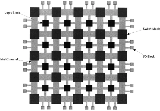
A 2-D FPGA consists of an array of configurable logic blocks (CLBs) that are
con-nected by a 2-dimensional grid of metal channels, as shown in Figure 1-1. Each CLB contains a small amount of digital logic in the form of Look-up Tables or LUTs which implement boolean logic functions using small access memories. A random-access memory of n bits can be used to implement any one of the 22' boolean functions that have n inputs and a single output. The outputs of the LUTs are also connected to registers whose output can be chosen instead of the direct LUT output. Thus a CLB can be programmed by a small amount of memory to implement sequential logic as well as combinational logic. The grid of metal channels connecting these CLBs together, contain switch boxes at the grid-points, which can connect the intersect-ing metal channels to each other usintersect-ing programmable switches. The programmable memory in the CLBs as well as the memory controlling the switches in the switch boxes, together form the configuration memory of the FPGA. Any logic circuit can be implemented in the 2-D FPGA by setting the memory in the CLBs to a particular state and connecting the CLBs in a particular manner. Therefore, any logic circuit
Logic Block,
Switch Matrix
VO Block Metal Channel.
Figure 1-1: Island-style 2-D FPGA
is functionally equivalent to a particular state of the configuration memory of the FPGA. For this particular state of the configuration memory, the FPGA behaves exactly like the mapped circuit for all possible inputs to the circuit. The individual components of the 2-D FPGA architecture are described in detail below.
1.2.1
Configurable Logic block
The Configurable Logic Block (CLB) as shown in Figure 1-2 contains the boolean logic that are the equivalent of gates in an ASIC circuit. The logic consists of multiple
Look-Up Tables (LUTs) and flip-flops. A LUT is a 16-bit SRAM accessed by a 4-to-1
MUX tree, representing a boolean logic function with four inputs and one output. The output of the LUT is also connected to a flip-flop and a 2-to-1 MUX is used to choose between the direct LUT output and the latched output. The latched output is
Internal
structure of CLB
161bhSRAM
Flip-flop 1&to-1 MUX
PLB
Figure 1-2: Configurable Logic Block
tables (LUTs), 16 block input pins and 4 block output pins. The 16 block input pins
are internally muxed into the inputs of the LUTs. Hence the block input pins are
logically equivalent i.e. a router can assign any one of the 16 block input pins to a
particular LUT input pin. This allows the router to dynamically pick a particular block pin as the desired sink depending upon the existing congestion constraints. The 4 block output pins that can be connected to any of the 4 LUT outputs through muxes. Hence the block outputs are also logically equivalent. The logic block also has internal routing between the logic block outputs and the inputs, which allows the LUT outputs to be muxed along with the block inputs to the LUT inputs. This feature
int~
~ ~
~
1-n1Il XOnl Input MMIX Jutt 1=4 * Ot3 Mig MIEIIiiEiE
11114
L- ! - F- MPL I Inpu 11. N \Xis later exploited in the packing stage, where a chain of LUTs in a boolean network can be packed together into a logic block. The internal routing circuitry allows such LUTs to avoid routing through switch matrices, reducing the delay between these
LUTs.
1.2.2
Switch Matrix
The regular grid of routing segments is connected at the grid-points by a collection
of switches known as a switch matrix. A switch matrix is a set of programmable
switches between the metal channels that can be configured to create any desired routing pattern. A switch matrix connects four metal channels, an X-channel that connects to the left of the switch matrix, an X-channel that connects from the right, a Y channel that connects from above and a Y channel that connects to the bottom of the switch matrix. Each of these channels usually has the same number of tracks W, which is known as the channel width of the FPGA. Therefore each side of the switch matrix has W pins that have to be connected to each other in some routing pattern. The switch flexibility F, of a pin on some side of a switch matrix is the number its connections to pins on the remaining sides of the switch matrix. Figure 1-3 shows a switch matrix where the pin East-1 has F, = 4, North-1 has F, = 3 and West-1 and
South-1 have F, = 2.
A popular switch matrix architecture is the disjoint switch architecture which is shown in Figure 1-5. In Figure 1-5, it can be seen that when the pins on a side of the switch matrix are numbered from 1 to W, a pin numbered i on one side of the SM connects only to the pins numbered i on the other three sides of the switch matrix. Hence the constraint on the routing pattern is that no pin i on one side can connect to a pin
j
on another side for ij.
Another example of a switch architecture is theuniversal switch block where every set of nets satisfying the dimensional constraint,
which is a maximum number of W tracks in each channel, is simultaneously routable through the switch matrix. The choice of the switch matrix architecture can have a significant impact on the routability of the FPGA and consequently the performance of the FPGA. The connections between the pins of the switch matrix can be made
West_1-West_2-+
WestW-+
North-I North-2 North W
S S
South_1 South_2 South-W
4-East_1 East_2 East-W
Figure 1-3: Switch block pins with different switch flexibility [14]
through a pair of tristate buffers or through a bidirectional pass transistor as shown in Figure 1-4. En En P noutas r nout2 Pass Transistor Inouti Inout2 -En Transmission gate EnI Inouta Inout2 En2 Tri-state buffers
Figure 1-4: Possible options for a switch cell
Any pin in the switch matrix can be driven by at most one out of the 3 switches that connect to it. The parasitic capacitance seen by this driving switch depends on the type of the switches that connect to this pin. When the connections are made through tristate buffers, the contribution made by each bidirectional connection to the capacitance seen by the driving pin is the sum of the input capacitance Cm and output capacitance Cmt of a tristate buffer. Therefore capacitance encountered by a
net driver at a switch matrix pin due to the bidirectional switches alone, is given by
CGi=
3
x(Cin
+Cout)
This capacitance value is seen by the driving switch regardless of whether the other tristate buffer connections are open or closed. When pass transistors are used to make the connections, the state of the other connections, either open or closed, determines the capacitance seen by the driving switch. In other words, in the case of pass transistor connection, the fanout at a pin determines the parasitic capacitance seen
by the switch driving the pin. The contribution of an open pass transistor switch
is only the overlap capacitance value of the transistor. On the other hand, a closed transistor switch, apart from the closed transistor capacitance, exposes the entire capacitance tree behind this switch, up to the points where buffers are encountered.
West-1-+
WestL2-*
WestW-+
North_1 North_2 North W
S
South_1 Soth-2 SouthW
East_1 - East_2
w- EastW
1.2.3
Channels
The metal channels that form the interconnect of the 2-D FPGA consist of two types of channels, namely the X and Y channels. Each channel contains wire tracks that can be individually driven by a source. The wire in each track is broken up into a multiple wire segments that have the same characteristics. It is found to be be more beneficial to use segments of different lengths rather than a single uniform length throughout the FPGA [26]. This allows the router connecting two CLBs in the
FPGA, to choose the type of segment depending on the physical distance between the
two CLBs. 'Long' wire segments that can span multiple switch matrices, bypassing intermediate switch matrices, are ideal for connecting CLBs that are far apart in the FPGA. On the other hand, to connect CLBs that are very close to each other, 'long' segments with a higher wire capacitance, result in greater delay compared to shorter segments.
A wire segment is characterized by the following properties:
" Length - The wirelength of the segment is measured in units of the distance between two adjacent switch matrices. For example, a wire segment of length 2 connects two switch matrices that are separated by a single switch matrix. A segment of length 4, connects two switch matrices in a row or column, separated
by three switch matrices.
" CLB population - When a wire segment spans across N switch matrices and is connected to the corresponding CLBs in only M out of the N switch matrices, the CLB population is given by M.
" Switch population - For a wire segment that spans across M switch matrices
and connects through switches to only M out of them, the switch population is given by M.
The different types of segments used in the 2-D FPGA are summarized in Ta-ble 1.1.
Length Number of CLB Number of SM Number of
spanned SMs population connected CLBs population connected SMs
1 2 1.0 2 1.0 2
2 3 1.0 3 0.66 2
4 5 0.6 3 0.4 2 Table 1.1: Segment types
" Channel width, which is the number of wire tracks within the channel
" Segment types -The different types of metal wire segments that form the chan-nel
* Segment distribution - The proportion of each of these segment types in the channel and how these segments are interleaved
" Segment staggering - The optimal orientation of the start points of each of these segment types for maximum routability
Staggering of tracks
A metal channel of an FPGA consists of W individual tracks where W is the global
channel width of the FPGA. When laying out the tracks of a particular segment type
within a channel, care must be taken not to start every track at the same grid location in the channel. To ensure greater routability, the "start points" of the segments in a channel have to be adjusted based on the length of the segment. To explain this concept further, a coordinate system must be defined for the FPGA. Let the grid point at the lower left corner in the bottom most layer of the FPGA have co-ordinates (1, 1). The grid-point to its right on has coordinates (2,1) and the grid-point above it on the same layer has coordinates (1, 2). An X channel has the same y-coordinate as the grid-points it passes through and a Y channel has the same x-coordinate as the grid-points it passes through. An ideal adjustment of the segments of a particular type would shift the start point of a segment of a particular track in channel
j
+ 1back by one grid-point relative to its start point in the same track in channel
j.
type, the segment start-point for the Zth track out of the n tracks, is defined as
L
segstart = (closestInteger(i * -))%L + 1
n
where closestlnteger(x) is the closest integer to a given real value x. Among all the grid points spanned by this X channel, a grid point (x, y) that marks the start of such a segment has the property
x - (x + y - segstart + L)%L= 0
Similarly, the start point
satisfies the property
of a Y segment of length L and segment start-point segstart
y - (x + y - segstart + L)%L = 0 Segment startpoints 7 A / / / /
Figure 1-6: Staggering for a segment of length 4
As can be seen from the symmetry in the start point calculations, the entire interconnect grid consists of X and Y that start and end at the same locations. There are no segments in the interconnect that end at a grid-point and are unable to connect to the segments in the other dimensions. This ensure high routability that proves to be very useful when routing complex circuits.
1.3
Overview of 3-D Integrated Circuits
As mentioned before, the regularity of the FPGA interconnect is the main reason for its low performance compared to ASICS. A technique to improve the performance of the FPGA interconnect is three-dimensional integration of the transistors of the
FPGA.
The motivation for 3-D circuits is that the addition of an extra dimension to the circuit can significantly decrease the Manhattan distance between a source and a sink. In other words, a 2-dimensional circuit can be imagined to be folded over multiple times resulting in layers of circuits that are connected by the 3-D interconnect. Due to the decreased wirelength of paths, the circuit blocks are expected to shrink towards each other resulting in higher performance of the circuit. It is shown in [13] that 31% to 56% speed improvement can be achieved with 3-D integration. Also the power dissipation of a circuit depends quadratically on the operating voltage of the circuit
Vdd while the performance depends linearly on Vdd. Hence a higher circuit performance in 3-D circuits can be lowered to the performance obtained in 2-D circuits for a much lower power dissipation by lowering the Vdd. Several previous works in literature have argued in favor of 3-dimensional integration [33] and particularly in FPGAs, [2],[13].
[15], [35], for these reasons. Several 3-D FPGA architectures have also been proposed
in the literature, [3], [4], [7],[8],[14], which demonstrate higher performance and lower power dissipation than 2-D FPGAs.
1.3.1
3-D
integration
In this work, the 3-dimensional layers of transistors are referred to as active layers and are often referred to in literature by terminology such as device layer, [15], tier,
[16], and stratum, [17]. There are several possible methods for 3-D integration of
active layers:
* Vertical Multi-Chip Module (MCM-V) - The dies are fabricated separately and bonded to a vertical Printed Circuit Board (PCB), [18] [19]. MCM-V connects
the dies from their periphery to PCB and these connections have larger delay compared to the on-chip connections.
" Ultra-thin chip stacking [20] [21] and multilayer thin-film packaging, [22] - In these methods, dies are thinned and bonded. Then the inter-layer connections are made through the periphery of the dies. While these methods offer better performance than MCM-V, the delay of an inter-layer connection is still large.
" Epitaxial 3-D integration - In this method silicon seeds are used to grow more transistors on the top of the current transistors, [23]. Another similar method uses solid-phase re-crystallization where amorphous silicon is deposited on the die and laser is used for crystallization. This method is used to fabricate high-density memories [24].
" Wafer bonding - The method used in the design of the 3-D chip in [14] is wafer bonding. During the design of each active layer, 3-D wires are connected through 3-D inter-layer vias. First, during the fabrication, different dies are fabricated with conventional methods. Then, they are bonded and 3-D connec-tions are made by etching. While this method allows high density of inter-layer connections, the delay and area overhead of inter-layer Vias are larger than on-chip Vias. Further discussion regarding the advantages and limitations of wafer bonding can be found in [14].
Chapter 2
3-D FPGAs
2.1
Architecture
This section describes in detail the architecture of the 3-D Field Programmable Gate Array. As in any FPGA, the 3-D FPGA consists of programmable logic blocks that are connected by an interconnect, which are both programmed by the configuration memory. The logic block of the 3-D FPGA is the same as a 2-D FPGA logic block but the 3-D interconnect methodology is quite different compared to the 2-D interconnect system. The key elements of the 3-D interconnect, the switch matrices and the metal channels, are described in detail in this section. The interconnect architecture described here is the first interconnect model that was conceived for the 3-D FPGA, known as the symmetric architecture. Later sections detail the optimizations that can be made to this architecture to achieve higher performance and overcome the problems that will be discussed at the end of this section. Since this work was primarily based on the physical parameters of the 3-D FPGA chip developed in [14], a summary of the relevant physical parameters is also presented here.
2.1.1
Global Architecture
A 3-D FPGA as shown in Figure 2-1 consists of multiple layers of logic blocks and
lattice of switch matrices that are connected by the metal interconnect. The 3-D interconnect consists of the horizontal X and Y channels and the vertical Z channels. Each logic block can connect to any horizontal or vertical wire segment that passes through the switch matrix at its location. The I/O pads of the FPGA are present along the periphery of the topmost layer as this layer alone is directly accessible by any off-chip source. The FPGA has an I/O ratio of 4 which means that four I/O pads are present in place of a single logic block in the I/O periphery.
Configurable Logic Block
X channel Y channel
Switch
MatrixZ channel
Figure 2-1: 3-D FPGA architecture
2.1.2
Symmetric interconnect architecture
The symmetric interconnect is a direct extension of the 2-D FPGA's interconnect system to 3 dimensions, with symmetric connections between the channels in all three dimensions. The vertical channel is simply an identical third dimension added to the 2-dimensional interconnect system. The vertical segments have the same segment properties such as number of spanned CLBs, CLB population and switch population, as the horizontal segments. However, as shown later, such a simple extension of the standard 2-D architecture to 3 dimensions has its own disadvantages. Hereafter in this work, this architecture will be referred to as the 3-D symmetric FPGA architecture.
2 W W WW wS 122 W 2 1
Figure 2-2: 3-D Switch Matrix [14] Switch matrix
The switch matrix (SM) or the switch box connects the intersecting horizontal and vertical wire segments at a grid-point in the lattice. A 2-D switch matrix has four sides which connect the X and Y segments to each other. However, the 3-D switch matrix as shown in Figure 2-2 has a hexagonal geometry owing to the fact that it connects to the four horizontal segments lying in the same layer and two vertical segments that intersect at this layer. The 3-D switch matrix has W pins of each of its six sides that connect to the respective tracks of the channels, where W is the channel width. The choice of the switch matrix topology is the disjoint switch architecture. Thus the flexibility of this switch matrix is 5 since each pin connects to exactly 5 other pins. The connections between the pins of the switch matrix are bidirectional and are made through a pair of tristate buffers or pass transistors. Therefore, the capacitance seen
at any pin in this switch matrix by a net driver is
Cgn = 5 x (Cin + C0u)
From the description of the 2-D FPGA's switch matrix in the previous chapter, it can be seen that the capacitance at a pin of the 3-D switch matrix is 5/3 times the capacitance seen at a pin of the 2-D switch matrix. Therefore, the additional
connectivity in the 3-D switch matrix comes at the cost of increased downstream
capacitance at every pin.
Interconnect channels
The segments used in the 3-D symmetric FPGA, as shown in Figure 2-3 are identical to those used by the 2-D FPGA, shown in Table 2.1. The connections between the segments and the CLBs are made through tristate buffers to isolate the capacitance
due to the select logic between the switch matrix pins and the block pins.
Length Number of CLB Number of SM Number of
spanned SMs population connected CLBs population connected SMs
1 2 1.0 2 1.0 2
2 3 1.0 3 0.66 2
4 5 0.6 3 0.4 2
Table 2.1: Segment types
Staggering of tracks
The staggering of the tracks in the 3-D symmetric interconnect is also an extension of the track staggering seen in the 2-D FPGA. For a X segment of length L in a channel having n tracks of this particular segment type, the segment start-point for the Zth track out of the n tracks, is now defined as
L
segstart = (closestlnteger(i * -))%L + 1
Segment of length one
Segment of length two
4
Segment of length four
Figure 2-3: Different types of segments used in the 3-D FPGA
where closestlnteger(x) is the closest integer to a given real value x. The grid point
(x, y, z) that marks the start of this segment has the property
x - (x
+
y+
z - segstart + L)%L = 0Similarly, the start point of a Y segment of length L and segment start-point segstart satisfies the property
y - (x + y + z - segstart + L)%L = 0
while a Z segment of length L and segment startpoint segstart starts at grid-points satisfying
z - (x + y
+
z - segstart + L)%L = 0Figure 2-4 shows the staggering in the 3-D interconnect for four tracks that are of the same segment type having a length of 4.
2.2
Physical parameters
The 4mm x 4mm 3-D FPGA chip with 3 active layers was designed in the Lincoln Lab
3-D FDSOI process. The hardware design of the chip and the detailed circuit design
of the chip can be found in [14]. This section presents only the physical parameters and architectural features that are necessary for the design of the 3-D FPGA CAD tool and further architectural exploration.
The physical parameters used by the CAD tool for timing calculations can also be found in [14]. From [14], it can be seen that the length of the vertical Z channel and consequently its segment capacitance is much smaller than that of the horizontal channels. More importantly, the output resistance of a tri-state buffer or the equiva-lent resistance of a pass transistor is nearly 7 times the resistance of a wire segment that spans a single tile. The timing calculations for the 3-D architecture shown below reflect the effect of such high switch resistance to segment resistance ratio.
2.3
Delay analysis
While the 3-dimensional nature of the interconnect provides greater routability, it comes at a cost of increased parasitic capacitance for each segment. In a 2-D switch matrix, a driving switch of a wire segment sees only the capacitance resulting from three other connections in every switch matrix that the segment connects to. However, in switch matrix of the symmetric architecture, the driving switch of a segment sees the capacitance due to five other connections in every connected switch matrix. The
Segment startpoints
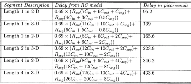
Resistance-Capacitance model equations for each of the segments in Table 1.1 is constructed below in Table 2.2.
Table 2.2: Comparing segment delays in 2-D and 3-D
Segment Description Delay from RC model Delay in picoseconds
Length 1 in 2-D 0.69 x (Rsw(7Cin ± 6Cout + Cseg)+ 95.2
Rseg(4Cin + 3Cout +
O.SCseg))
Length 1 in 3-D 0.69 x (R3s(11Cin + 1 0Cout + Cseg)+ 139
Rseg(6
Cin
+ 5Cout + O.5Cseg) )Length 2 in 2-D 0.69 x (Rsw(8Cin + 6Cot + 2Cseg)+ 165.6
Rseg(9Cin + 6Cout + 2Cseg))
Length 2 in 3-D 0.69 x (Rsw(12Cin +
1
0ot + 2Cseg)+ 223.9Rseg(13Cin + 10Cout + 2Cseg))
Length 4 in 2-D 0.69 x (Rsw(8Cin + 6Cout + 4Cseg)+ 346.2
Rseg(18Cin + 12Cout +
8Cseg))
Length 4 in 3-D 0.69 x (Rsw(12Cin + 1 0
Cout
+ 4Cseg)+ 433.6Rseg(26Cin + 2 0
Cout + 8Cseg)) I
The Elmore delay model is used to calculate the delay for a signal to traverse a given wire segment. RW is the output resistance of the tristate buffer, Cin and
Cout are the input and output capacitances of the tristate buffer, Reg and Ceg are
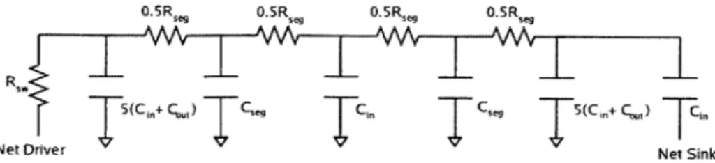
the resistance and capacitance of a wire segment of unit length. An example of the Elmore delay calculation is shown in Figure 2-5 for a segment of length 2 in the 3-D interconnect.
The physical values from [14] are substituted in the RC equations shown in Table
2.2, which yield the delay values for each segment type. As seen from Table 2.2, a 3-D
horizontal segment of the same length, switch and logic block populations has more delay than a 2-D segment with similar characteristics. This observation indicates the need for more optimization in the interconnect architecture in order to achieve high performance in 3-D FPGAs.
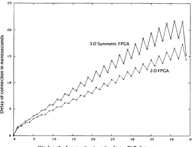
As a consequence of the segments in the symmetric 3-D FPGA having more delay than their 2-D counterparts, the delay of the point-to-point connections in the FPGA also increases. Figure 2-6 shows the average delay of the point-to-point connections of both a 2-D FPGA and a 3-D FPGA with 5 layers, in the increasing order of their
.5R,, 0.SR .5R, 0.5Re
Rsw
I(Cn+C.)
Cg C
77
C C,.) cinNet Driver Net Sink
Figure 2-5: RC model of segment of length 2 in 3D
Tdl = 0.69 x (R,. x 5 x (Cin + C1 t) + (Rsw + 0.5 x Reg) X Cseg +
(Rsw + Rseg) X Cin + (Rsw + 1.5 x Rseg) X Cseg +
(Rsw + 2 x Rseg) x 5 x (Cin + Cout) + (Rsw + 2 x Rseg) x Cin) 0.69 x (R8w x (12 x Cin + 10 X Cout + 2 X Cseg) +
Rseg X (13 x Cin + 10 X Cout + 2 X Cseg))
wirelength. It can be seen from Figure 2-6 that the average delay of 3-D connection is considerably greater than a 2-D connection of the same wirelength. Therefore, a circuit will run faster on the symmetric 3-D FPGA only when its critical path has a much lower wirelength than the circuit's critical path in a 2-D FPGA. of the circuit in a 2-D FPGA. Though the wirelength of each connection is expected to be lower in the 3-D FPGA, the higher delay of the 3-D segments is a strong mitigating factor in the performance of the symmetric 3-D architecture.
In the 3-D FPGA, circuit blocks are expected to come much closer spatially to each other than in the 2-D FPGA, due to extra degree of freedom in connecting the blocks. In some sense, the 2-D circuit can be thought of as being folded over in a 3-D FPGA over multiple layers. Since the main advantage in the symmetric 3-D FPGA is the decrease in wirelength, it is necessary to study the relation between the connection wirelengths and the number of layers in the FPGA. Using our 3-D CAD tool which is detailed in the next chapter, the circuits from the MCNC'91 benchmark suite were mapped to 3-D symmetric FPGAs of sufficient dimensions. From the placed and routed circuit, the wirelengths of all their point-to-point connections, in units of the inter-CLB distance, were extracted. Figure 2-7 shows the individual and combined histograms of the wirelengths of the connections in the circuit frisc in the 2-D and
25 20 3-D Symmetric FPGA 0A 0 15 2-D FPGA .0 W 5 10 15 20 25 30 35 40 45
Wirelength of connection in units of inter-CLB distance
Figure 2-6: Average delay of point-to-point connections
the 3-D symmetric FPGA. As can be seen from Figure 2-7, 3-D integration certainly reduces the wirelength of the connections in the mapped circuit compared to the 2-D FPGA.
However, a 3-D FPGA must be able to achieve the same reduction in the delay histogram as well in order to guarantee higher performance than the 2-D FPGA. Figure 2-8 shows the individual and combined delay histograms for the circuit des mapped to both a 2-D and a 3-D symmetric FPGA. The delay intervals in the delay histograms are of 0.5 nanoseconds. It can be seen from Figure 2-8 that the delays of the point-to-point connections are also reduced in the 3-D symmetric architecture, but not as significantly as the wirelength distribution.
9 5 t 15 20 a3 39 35 40 45
Wirelength of connection in units of inter-CLB distance
Wirelength histogram for 'frisc' in 2-D FPGA
9 5 1@ 1 Re 25 30 35 40
Wirelength of connection in units of inter-CLB distance
Wirelength histogram for 'frisc' in 3-D symmetric
2-D FPGA
-3-D Symmetric FPGA
5 10 is 20 25 3 35 40 45 so
Wirelength of connection in units of inter-CLB distance
Combined wirelength histogram for 'frisc'
45
FPGA
Figure 2-7: Wirelength histograms for circuit frisc
0 0 0 E z 0 .0 E z
I-
.
I
i
0 t; 0 0 E z 600 409 13e 900 40 308 .00 100 900 700 500 40. 300 2 4 6 a is 12 14 16
Delay of connection in nanoseconds
Delay histogram for 'frisc' in 2-D FPGA
Delay of connection in nanoseconds
Delay histogram for 'frisc' in 3-D symmetric FPGA
2-D FPGA 3-D Symmetric FPGA
I
I
2 2 4 6 8 1 12 14 16 1 20
Delay of connection in nanoseconds
Combined delay histogram for 'frisc'
Figure 2-8: Delay histograms for circuit frisc
12 14 16 19 le 140e 1200-100 200 0 2 4 6 9 10 ,40 100 600 1600 1488 -1200 --1008 800 -- 600-400 200 a 111M ..
Chapter 3
CAD for 2-D and 3-D FPGAs
A CAD tool for an FPGA accepts an RTL description of a circuit and an architectural
description of the FPGA for generating a configuration bitstream that can be loaded onto the FPGA. This complex problem of mapping a circuit to an FPGA is broken down into a sequence of subproblems or stages as shown in Figure 3-1. Each of these problems can be reduced to some classical theoretical problems that have been extensively researched. Each stage has its own optimization goal which is related to the ultimate goal of satisfying space and performance requirements for the circuit when mapped to the FPGA.
Several CAD tools have been proposed earlier for both 2-D FPGAs [26] and more recently for 3-D FPGAs, [5],[6], [13]. All these CAD tools have a common tool flow which will be detailed in this chapter. This work also proposes a complete CAD tool for 3-dimensional FPGAs by extending a popular 2-D FPGA CAD tool known as the Versatile Place and Route (VPR) CAD tool [26]. The objective of this CAD tool is to facilitate the exploration of the 3-D FPGA architecture which is a relatively new architecture compared to the 2-D FPGA.
The first part of this chapter provides an introduction to the standard 2-D FPGA
CAD tool flow and the second part of this chapter describes the contributions of this
work in the design of a 3-D FPGA CAD tool. Many of the stages in the FPGA tool flow are independent of the architecture and are therefore identical in both the 2-D and the 3-D FPGA CAD tool. Only one important stage of the VPR tool, known
as the placement stage and a graphical representation of the circuit used in the tool, known as the Routing-Resource graph, are modified to convert it into a 3-D FPGA
CAD tool. The CAD stages preceding the placement stage and the routing stage that follows the placement, are completely retained from the original tool.
The following section describes the standard FPGA CAD tool flow that is
ap-plicable to both 2-D and 3-D FPGAs. The later section describes in detail, the
modifications proposed by this work to the placement stage.
3.1
Generic FPGA CAD tool flow
3.1.1
Logic synthesis
The first stage known as synthesis converts the high-level circuit description into a
gate-level netlist. A logic optimization process is used to remove the redundant logic
from the netlist and simplify the logic whenever possible. The gate-level netlist is then
converted into a network of Look-Up Tables (LUTs) with the objective of minimizing
the number of LUTs or the expected performance of the circuit. This problem of
converting a gate-level netlist to an LUT-level netlist is called technology mapping
and has been extensively studied in literature, [30] [31]. This work uses the Berkeley
MVSIS tool for the purpose of synthesizing a network of 4-input LUTs from an RTL level circuit specified in the Berkeley Logic Interchange Format (BLIF).
3.1.2
Packing
Every CLB in the 3-D FPGA contains 4 LUTs as described in the previous section.
The LUTs in the boolean network obtained from the logic synthesis stage need to
be clustered into groups of 4 LUTs, to be mapped to the CLBs of the FPGA. The
optimization goal in this stage is to pack lookup tables sharing common signals such as
inputs and outputs, into a single logic block. When a logic block containing LUTs with
shared signals is mapped to the architecture, fewer nets need to be routed to the CLB
BLIF description of circuit
Logic synthesis
LUT Packing
Block Placement
Net Routing
Generate configuration bitstream
Figure 3-1: Standard CAD tool flow for FPGAs [26]
equivalently a graph partitioning problem with constraints on the maximum partition size. The packing problem also has several good solutions in the literature, [30], [31]. The VPR tool itself contains a timing-driven packing tool known as TV-Pack that packs an LUT netlist into logic blocks of a specified size. The TV-Pack tool assumes no knowledge of the underlying architecture except the capacity of the logic block and is therefore used without any modification for the 3-D FPGA.
3.1.3
Placement
The third stage of the design flow, known as the placement problem, is the first stage in the tool flow that is dependent on the architecture of the FPGA. Since this stage alone will be modified for 3-D FPGAs, this stage is described in more detail. The placement problem requires the mapping of each logic block produced by the packing stage to a specific CLB location in the 3-dimensional grid. The goal in this stage is
to find a mapping of the logic blocks to CLBs that minimizes the delay of the critical
path in the mapped circuit.
In the case of a sequential circuit being mapped to the FPGA, the critical path is the path with the maximum delay between any two flip-flops in the FPGA. Such a path may traverse through several switch matrices and through several combinational logic blocks before reaching its destination. In this case, the critical path delay can be further divided into the net delay and the logic delay. The net delay is the sum of the delays of all the CLB-to-CLB connections on the path, while the logic delay is the sum of the delays incurred in passing through the internal logic of all the intermediate CLBs. In the case of a combinational circuit being mapped to the FPGA, the critical
path is the path with the maximum delay between an input and output pad of the
FPGA. The critical path delay is the minimum period of the signal used to clock the circuit and is therefore a direct measure of the performance of the circuit.
The placement of logic blocks in the FPGA can be considered as an arrangement of logic blocks as well as empty locations in the 3-dimensional grid of CLBs. It can be seen that finding the exact permutation of logic blocks in n CLB locations to yield optimum performance is a problem of complexity O(n!). Hence, heuristics are employed in order to find a sub-optimal solution in a reasonable duration of time.
There are three primary approaches to solving this problem:
* Partitioning-based solutions or min-cut solutions
Placement by recursive partitioning repeatedly divides a given circuit into sub-graphs in order to minimize the objective function. With each partitioning of the circuit, the CLB grid is also partitioned. Each subgraph is then as-signed to a partition of the CLB grid. This process proceeds recursively till each subgraph is assigned to a unique CLB in the grid. The total number of cuts between the subgraphs is an estimate of the total wirelength of the circuit whose minimization is an objective of the placement process. Most partition-ing based techniques employ some form of the prototype iterative heuristic of Kernighan and Lin (KL) [32] which uses a pair-swap move structure. During
each pass, every block is moved exactly once between two partitions. At the beginning of the pass, all blocks are free to be swapped. Iteratively, the pair of the unswapped blocks with highest gain is swapped and the cost of the new partitioning is updated. After all the blocks have been swapped, the lowest-cost partition encountered throughout the pass is restored and a new pass begins.
" Analytic solutions followed by local iterative improvements
The placement problem can be formulated as a sequence of quadratic program-ming problems derived from the entire connectivity information of the circuit. The problem can then be solved through a combination of global optimization and rectangle dissection, which is based on the partitioning techniques.
* Simulated Annealing
Simulated Annealing (SA) is a stochastic minimization technique that is based on the metallurgical annealing process used to cool molten metal very gradu-ally to produce a metal crystal lattice with lower internal energy. The VPR
CAD tool contains an SA placement algorithm for 2-D FPGAs which has been
extended to the case of 3-D FPGAs. This SA placement algorithm is an ap-plication of the generic SA algorithm shown in Algorithm 1, to the problem of CLB placement in the FPGA.
The SA placement process explores the placement solution space by minimizing a chosen objective function F of the placement, through a large number of local changes. The SA process has a parameter known as the temperature, T, which dictates the likelihood of accepting a local change to the current placement. The SA process starts with an initial random placement of the circuit's blocks in the FPGA and an initial value of T. The SA process then makes a certain number of random swaps among the CLBs of the FPGA at the current temperature T, with each swap involving at least one CLB which is used in the current placement. Each swap causes a change in the chosen objective function value, which is immediately recalculated. The change in objective function value is AC = F(PlacementNew)~-F(Placementold) . The swap
Algorithm 1 Generic SA algorithm 1: Start with random initial state
2: T <- 1
3: while T ;> Tcetrf do
4: for i =
I
to N do5: Move to an adjacent state in the solution curve
6: Calculate new value of objective function, C
7: AC = CNew - Cold
8: if AC
<
0 then9: Accept the new state
10: else
11: Generate random value r, 0 < r < 1
AC
12: if e- > r then
13: Accept the new state
14: else
15: Reject the new state
16: end if
17: end if 18: end for
19: Update T based on annealing schedule 20: end while
AC
is then accepted with a probability e--. At higher temperatures, this probability is
very high which allows the SA process to accept inferior solutions and thereby explore the solution space. The temperature is then either scaled down by a pre-determined factor (fixed annealing schedule) or by a schedule based the current progress of the placement process (adaptive annealing schedule). As the temperature decreases, the probability of a swap that results in an inferior value of F becomes very low. This allows the SA process to quickly converge to a sub-optimal placement solution that is very close to the optimal placement solution. The objective function F chosen by the VPR placement process is a sum of the delays of all the connections in the circuit, weighted by the criticality of each connection. The criticality of a connection
P between a net source and a sink in a circuit with critical path delay D, is defined
as
Criticality(P) = Slack(P)
D
across the connection and the required time of the arrival of the signal at the sink, in order to propagate to the next connection in the circuit. For every connection in the critical path of the circuit, the slack would be 0 since the critical path has the greatest delay among all the paths in the circuit. Therefore the objective function F known as the timing cost function, for n connections, Ci ... Cn is given by
n
F = Criticality(Ck) x Delay(Ck)
k=1
An important implication of this timing cost function is that if a CLB swap changes the critical path of the circuit, then the timing cost needs to be recalculated. The new critical path delay value would have to be calculated and the criticality values of all the connections in the circuit would have to be updated. But this would considerably slow down the computation in the placement process. Hence the tool assumes that the critical path delay value is not greatly affected by a block of swaps which can all be made without updating the criticality values.
3.1.4
Routing
The last computational stage of the CAD flow is the routing stage in which all the nets of the FPGA are routed between their sources and sinks. After the logic blocks and I/O pads of the circuit have been placed in the FPGA's CLBs, the router determines which of the FPGA's switches should be turned on to make all the required pin-to-pin connections. Once again, the optimization goal is to minimize the delay of the critical path in the circuit. The VPR router uses a optimized version of the PathFinder algorithm, [26], to quickly route the connections in the circuit. As later described, this stage is retained without modifications in the 3-D FPGA tool by simply altering the abstraction of the FPGA architecture that is used by this stage. This abstraction, known as the Routing Resource graph, is described below.
Routing-Resource graph
The VPR router, based on the Pathfinder algorithm, operates on a graphical abstrac-tion of the FPGA architecture known as the Routing-Resource (RR) graph. Every wire segment and I/O pin is represented by a node in this graph and directed edges between these nodes explicitly model the connectivity information of the FPGA. The bi-directional switches are represented by pairs of directed edges between the nodes. As seen in Figure 1-2, the internal routing of the CLB makes it possible for any logic block input pin to connect to any input pin of any of the 4 LUTs in the CLB. Thus, the input pins of the CLB are logically equivalent. Similarly, any of the LUT out-put pins can connect to any of the outout-put pins of the CLB which are also logically equivalent. To expose this property of the logic block's pins to the router, a source and sink node are created in the RR graph for every CLB. The input pins of a CLB have directed edges to the sink node while directed edges exist from the source node to the output pins of the CLB. Every RR node stores additional information about its physical counterpart, such as resistance, capacitance, track or pin number and so on. Timing-driven routing can then be performed directly on the RR graph using the physical information in the nodes.
3.2
Contributions to 3-D FPGA CAD flow
3.2.1
Routing-Resource graph for 3-D FPGAs
This work extends the VPR CAD tool to 3-D FPGAs by modifying only the place-ment stage of the tool and by retaining all the remaining stages of the tool. The stages preceding the placement stage can be retained with no effort, but the routing stage that follows the placement does depend on the underlying FPGA architecture. However, the routing tool abstracts the FPGA architecture into a Routing Resource graph (RR graph) which is then used by the VPR implementation of the PathFinder algorithm. Therefore to use the VPR router without any modifications, the RR graph corresponding to the 3-D FPGA is generated. The generation of the RR graph of
the 3-D FPGA is a painstaking process of converting every pin and wire segment in the FPGA into a RR node and connecting all the RR nodes to reflect the 3-D connectivity. The CAD tool proposed by this work for 3-D FPGAs can take the architectural description of any 3-D FPGA and automatically generate the corre-sponding RR graph. This allows the VPR router to integrate seamlessly with the modified placement stage. Figure 3-2 shows a slice of the 3-D FPGA architecture and the corresponding subgraph of the RR graph generated for the 3-D FPGA ar-chitecture. It can be seen that the additional connectivity of the 3-D interconnect is exposed directly to the router through the RR graph.
Sink B
Input pin B
Y chan nel Input pin C
,ii P111 111W*Sink C
= Sorce AX channel
Source
AZ chan nelOutput pin A I nput pin D
Sink. D
Figure 3-2: Translation of architecture to Routing-Resource graph
3.2.2
Modifications to VPR placement
In order to extend the VPR placement to the case of 3-D FPGAs, several internal data structures of the VPR code base have been modified to reflect the 3-D architecture. These structures include the CLB matrices which now represents a 3-dimensional grid of CLBs, switch matrix representations, I/O periphery information and CLB to track connectivity, among several others. Apart from these modifications which are necessary to extend the VPR placement to 3-D FPGAs, some changes have also been introduced in the SA algorithm used in the placement, which are described below.
CLB B
Non-adaptive schedule
The actual implementation of the SA placement process is highly dependent on the problem space and the choice of parameters can make a significant change in the runtime of the process. These parameters include the annealing schedule, the number of swaps attempted at each temperature and the exit criterion for the process. The VPR placement for 2-D FPGAs uses an adaptive annealing schedule that adjusts itself and the initial parameters, based on the ratio of the number of successful swaps to the total number of attempted swaps at a particular temperature. The VPR placement algorithm and its parameters are designed to keep this success ratio nearly constant and equal to 0.44, [26]. However, when the 2-D placement algorithm is extended to the case of the 3-D placement, the parameters specified for the 2-D placement algorithm are not suited to maintain the success ratio is a constant. In fact, finding an ideal set of parameters to maintain a constant success ratio for the 3-D placement becomes quite a tedious process. Hence a small compromise is made in the performance of the placement algorithm implementation by choosing a simple non-adaptive SA schedule that makes a definite number of temperature steps. This allows all the parameters of the SA algorithm to be scaled linearly depending on the current temperature, initial temperature and the exit temperature.
Two-stage Simulated Annealing
The timing cost function specified in the VPR placement algorithm is intended to reduce wirelength and congestion in the final routing, since the evaluation of the critical path after every swap of CLBs is impractical. However, the placement algo-rithm must still maintain the global objective of reducing the critical path delay of the final circuit. In order to deal with the dual objectives of minimizing the timing cost function and the critical path delay, a two-stage Simulated Annealing process as shown in Algorithm 2 is proposed. The two-stage SA process consists of :
9 A local SA process that performs small local improvements to the circuit by

![Figure 1-3: Switch block pins with different switch flexibility [14]](https://thumb-eu.123doks.com/thumbv2/123doknet/14193794.478628/18.918.226.669.119.482/figure-switch-block-pins-different-switch-flexibility.webp)
![Figure 2-2: 3-D Switch Matrix [14]](https://thumb-eu.123doks.com/thumbv2/123doknet/14193794.478628/27.918.199.662.120.529/figure-d-switch-matrix.webp)