HAL Id: hal-00691428
https://hal.archives-ouvertes.fr/hal-00691428
Submitted on 26 Apr 2012
HAL is a multi-disciplinary open access
archive for the deposit and dissemination of
sci-entific research documents, whether they are
pub-lished or not. The documents may come from
teaching and research institutions in France or
abroad, or from public or private research centers.
L’archive ouverte pluridisciplinaire HAL, est
destinée au dépôt et à la diffusion de documents
scientifiques de niveau recherche, publiés ou non,
émanant des établissements d’enseignement et de
recherche français ou étrangers, des laboratoires
publics ou privés.
Structural recovery of ion implanted ZnO nanowires
Guillaume Perillat-Merceroz, Fabrice Donatini, Robin Thierry, Pierre-Henri
Jouneau, Pierre Ferret, Guy Feuillet
To cite this version:
Guillaume Perillat-Merceroz, Fabrice Donatini, Robin Thierry, Pierre-Henri Jouneau, Pierre Ferret,
et al.. Structural recovery of ion implanted ZnO nanowires. Journal of Applied Physics, American
Institute of Physics, 2012, 111 (8), pp.083524. �10.1063/1.4704697�. �hal-00691428�
G. Perillat-Merceroz,1, 2,a)F. Donatini,3
R. Thierry,1
P.-H. Jouneau,2
P. Ferret,1
and G. Feuillet1
1)CEA, LETI, Minatec Campus, Grenoble, 38054, France
2)CEA INAC/UJF-Grenoble1 UMR-E, SP2M, LEMMA, Minatec Campus, Grenoble, 38054,
France
3)Institut N´eel, CNRS and Universit´e Joseph Fourier, BP 166, 38042 Grenoble Cedex 9,
France
Ion implantation is an interesting method to dope semiconducting materials such as zinc oxide provided that the implantation-induced defects can be subsequently removed. Nitrogen implantation followed by anneals under O2 were carried out on zinc oxide nanowires in the same conditions as in a previous study on bulk ZnO [J. Appl. Phys. 109, 023513 (2011)], allowing a direct comparison of the defect recovery mechanisms. Transmission electron microscopy and cathodoluminescence were carried out to assess the effects of nitrogen implantation and of subsequent anneals on the structural and optical properties of ZnO nanowires. Defect recovery is shown to be more effective in nanowires compared with bulk material due to the proximity of free surfaces. Nevertheless, the optical emission of implanted and annealed nanowires deteriorated compared to as-grown nanowires, as also observed for unimplanted and annealed nanowires. This is tentatively attributed to the dissociation of excitons in the space charge region induced by O2adsorption on the nanowire surface.
I. INTRODUCTION
For a decade, zinc oxide has aroused growing inter-est, especially because of potential applications in short-wavelength optoelectronics. This material is particularly interesting as nanowires, which are easily grown, with no catalysts, on various types of substrates such as sapphire, and by different growth methods such as metalorganic vapor phase epitaxy (MOVPE).1Among other potential applications, ZnO nanowires are studied for making light-emitting diodes (LEDs) because of the advantages they present over ZnO thin layers, related for instance to the presence of larger developed surfaces. Nanowire growth on large and conductive hetero-substrates such as silicon2 and metal3 is possible, and no extended defects are ex-pected (for example, none were observed in nanowires grown on sapphire).4,5 Furthermore, nanowires with ra-dial core-shell quantum wells can be grown, yielding large emitting volumes,6 and with a good internal quantum efficiency.7 Moreover, light extraction is naturally more efficient in nanowire LEDs than in thin layer LEDs.8 p-type doping of ZnO nanowires remains challenging, but p-type doping obtained in situ during the growth was reported, allowing the observation of a weak ultra-violet (UV) emission under current injection for p-n homo-junctions in ZnO nanowires.9,10 Finally, an electrically-pumped laser made of in situ Sb-doped p-type ZnO nanowires on a n-type ZnO thin film was demonstrated.11 Ion implantation is another way to dope ZnO, which offers the possibility to introduce dopants beyond their solubility limit. However this method degrades the op-tical and electrical properties because of the creation of structural defects,12 such as point defects13 and disloca-tion loops.14These defects can be removed by annealing, but the temperature must be sufficiently high to recover
a)Electronic mail: gperillat@gmail.com
a material without defects, and sufficiently low in order not to deactivate the dopants. Two publications reported on LEDs made from ZnO nanowires for which p-type doping was tried by ion implantation.15,16 In the first one, p-type doping was claimed through arsenic implan-tation followed by a 750◦C annealing for 2 h, with doses of 1014or 1015cm-2. For the higher 1015cm-2 dose, UV electro-luminescence (EL) was negligible compared to the red one. For the lower 1014cm-2dose, EL was obtained mainly in the UV range, but the signal was very noisy and appeared above a rather high voltage (6 V). The sec-ond publication concerns phosphor implantation with a 1014 cm-2 dose. After a 900◦C annealing for 2 h, UV EL was also measured, but once again only for high volt-ages and currents (a few tens of V and mA). Moreover, the EL may be due to a metal-insulator-semiconductor stack. These publications clearly call for an optimization of the annealing conditions of the implantation-induced defects.
Recovery of structural defects by annealing in ZnO nanowires has been studied for manganese, vanadium, and gallium implantations.17–19 For Mn implantation, it was shown by photoluminescence (PL) that nanowires recovered nearly the same luminescence as unimplanted ones after a 800◦C, 15 min annealing under vacuum.17 However, it was shown by transmission electron mi-croscopy (TEM) that the dislocation loops identified be-fore annealing did not disappear totally. For V implan-tation, a partial recovery of implantation defects after a 500◦C, 30 min annealing under O2 was observed.18 Concerning Ga implantation, a parametric study as a function of the implanted dose (from 5×10¹²to 1.5×1016 cm-2), and of the annealing temperature (from 450◦C to 700◦C) was carried out.19 For doses lower than 5×1013cm-2, implantation-induced dislocation loops dis-appeared after annealing under argon at 700◦C.
However, no comparison was made in these studies be-tween ZnO nanowires and bulk ZnO in terms of implan-tation defect recovery. Thus it is not known whether
2 implanting nanowires is advantageous or not compared
to bulk implantation. We previously demonstrated, for the bulk case, that dislocation loops induced by nitrogen implantation were hard to remove by annealing, leading to poor electrical properties.14However, the dislocations were shown to disappear just below the surface of the implanted substrate, suggesting that if implantation was carried out in thin enough nanowires, a total structural recovery could be possible. Moreover, despite numerous works on N implantation of bulk samples or thin layers, no study combines both TEM and optical spectroscopy concerning the removal of the nitrogen implantation de-fects, a crucial step to limit non-radiative losses in light-emitting devices.
In this paper, N implantation was carried out on nanowires using the same conditions as in our previous study on bulk implantation.14 This allows a direct com-parison of the defect recovery mechanisms. Annealing at different temperatures and for different times were performed. TEM and cathodoluminescence (CL) were used to compare spatially-resolved structural and optical properties of as-grown, implanted, implanted-annealed, and unimplanted-annealed nanowires. Implantation de-fect recovery is shown to be more efde-fective in nanowires compared with bulk material. Nevertheless, even if dis-location loops disappear after annealing because of the proximity of the free surfaces, the optical properties are not recovered compared to the as-grown nanowires. The optical properties are degraded similarly for unimplanted and annealed nanowires, although these do not contain any extended defects, possibly because of O2 adsorption on the nanowire surfaces.
II. EXPERIMENTAL DETAILS
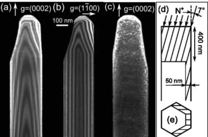
Nanowires were grown by MOVPE on sapphire. More details about the growth conditions and the structural characterizations are presented in previous articles.4,5,20 Two unimplanted parts of the nanowire sample were kept as references for TEM and CL studies: one as-grown and the other one annealed at 900◦C for 2 h under O2 at atmospheric pressure. On another part of the sample, three successive implantations at different energies and doses were carried out in order to obtain a flat nitrogen profile. Accelerating voltages of 50, 120, and 190 kV with respective doses of 4.1014, 8.1014, and 1015 cm-2 were used. The sample was tilted 7◦C relative to the ion beam direction. One piece of the implanted sample was annealed at 700◦C for 15 min, another at 900◦C for 15 min and the last one at 900◦C for two hours, under O2at atmospheric pressure. CL experiments were carried out at 30 kV and 10 K. TEM was done on a FEI-Tecnai microscope operated at 200 kV.
FIG. 1. Weak-beam TEM images of an as-grown nanowire with (a) g = (0002), with (b) g = (1¯100), and of (c) an implanted nanowire with g = (0002). Schematics of the im-plantation depth as simulated with the SRIM software21 (d)
in cross section, and (e) in a plane section of the nanowire bottom.
III. RESULTS
A. Structural properties
Weak-beam TEM images of as-grown nanowires with g = (0002), and with g = (1¯100) [Fig. 1 (a) and (b) respectively] exhibit only equal thickness fringes: neither stacking faults nor dislocations are present. Implantation-induced structural defects can be seen in Fig. 1 (c). In our previous work about N implantation in bulk ZnO, the same defects were observed.14 These are dislocation loops formed by agglomeration of Zn and O interstitials. But contrary to the bulk case, loops are present here not only in a 400 nm-thick layer below the top surface, but also on the side-walls of the nanowires because of the inclination of the ion beam [Fig. 1 (d)]. The nanowire density and height (around 5×106 cm-2 and 3 µm) are actually such that shadowing effects are negligible.
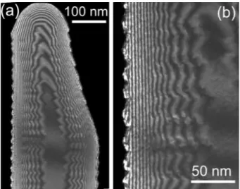
Figure 2 shows TEM images of implanted and annealed nanowires for two annealing conditions. For a 700◦C, 15 min annealing[Fig. 2 (a)], a 35 nm outer shell with no remaining dislocation loops is observed. Dislocations are still visible below the 400 nm zone under the top of the nanowire, because the implanted thickness on the sides is thicker (50 nm) than the recovered outer shell (35 nm). For a 900◦C 15 min annealing [Fig. 2 (b)] the outer shell is 70 nm wide, as observed for the sub-surface zone in the bulk case.14 Contrary to the 700◦C annealing case, there are no dislocations below the 400 nm zone under the nanowire top, because the recovered outer shell is thicker (70 nm) than the implanted shell on the sides (50 nm) (see also figure 6 (a)). As observed for the bulk case, loops are less dense but bigger with increased annealing, which is ascribed to a larger point defect diffusion at high temperature.14
FIG. 2. Weak-beam TEM images with g = (0002) of im-planted nanowires after annealing (a) at 700◦C for 15 min,
and (b) at 900◦C for 15 min.
FIG. 3. Weak-beam TEM images with g = (0002) of im-planted nanowires after annealing at 900◦C for 2 h, at two
different magnifications.
FIG. 4. Weak-beam TEM images with g = (0002) of unim-planted nanowires after annealing at 900◦C for 2 h, at two
different magnifications.
FIG. 5. 10 K CL spectra from the top of an as-grown nanowire (scale on the right axis), and from the tops of the implanted and annealed nanowires at 700◦C for 15 min, at 900◦C for
15 min, and at 900◦C for 2 h (scale on the left axis).
and annealed at 900◦C for two hours. The nanowire sur-face appears rough, and some defects are visible at the edges of the nanowire, but not in its core. It is thus unlikely that these defects are implantation-induced dis-location loops, because they should be present in the core too. Moreover, dislocations were shown to disappear in a 70 nm zone from the surface after a short 15 min, 900◦C annealing. Therefore, it is not expected that for a longer annealing, dislocations would be present in this zone. Figure 4 shows an unimplanted nanowire annealed in the same conditions (900◦C, 2 h under O2) for com-parison. The nanowire exhibits rough side facets instead of the perfectly flat ones for as-grown samples. Despite this, no structural defects are visible inside the nanowire. Consequently, the defects visible in figure 3 are probably due to an annealing-induced surface degradation of the implanted ZnO, as this was already observed for high dose arsenic implantation at a 1.4×1017cm-2 dose, after annealing at 1000◦C.22This stresses the fact that anneal-ing conditions have to be optimized: sufficient annealanneal-ings have to be performed in order to remove the implantation defects, but moderate annealings (short duration and low enough temperature) is desirable in order not to degrade the implanted ZnO. Moreover, moderate annealings are necessary not to deactivate the dopants.23For nanowires smaller than 140 nm or 70 nm in diameter, it is extrap-olated that no dislocations should be left after annealing at 900◦C or 700◦C respectively, for a duration of no more than 15 min. It is thus demonstrated that the elimina-tion of dislocaelimina-tions is facilitated by the proximity of the nanowire free surfaces, allowing shorter duration anneal-ings at lower temperatures, which is a clear advantage of nanowires compared to bulk material.
4
B. Optical properties
Figure 5 shows the CL spectrum taken on a 400 nm-long zone at the top of an as-grown nanowire (curve in red, with the scale on the right axis). Apart from the excitonic peaks around 3.365 eV,24 a peak at 3.31 eV is present, with its one longitudinal optical phonon replica separated by 72 meV. The exact origin of the 3.31 eV peak has been debated a lot (see for example Ref.25,26), and is beyond the scope of this paper: we will only dis-cuss the relative intensities of the peaks depending on the different annealing conditions. The CL spectrum of an as-grown nanowire is compared to that of the top part of an implanted and annealed nanowire. Upon implan-tation and annealing, a drastic decrease of the emission is observed (by a factor of 200 for the 3.31 eV peak af-ter annealing at 900◦C for 2 h). For higher temperature or longer annealing, the emission is slightly improved: considering for instance the 3.31 eV peak, there is an in-crease by a factor of three between the emission of the nanowires annealed at 700◦C for 15 min and at 900◦C for 2 h. The 3.36 eV excitonic emission recovers more slowly and appears only when the density of dislocations is low enough: it is nearly absent for nanowires implanted and annealed at 900◦C for 15 min, whereas it is present, al-though weaker than for as-grown nanowires, for a longer annealing of two hours at 900◦C. In the implanted and annealed samples, it is impossible to detect the presence of the donor acceptor pair transition attributed to N at 3.235 eV,24because of the phonon replica of the 3.31 eV peak around 3.24 eV.
Figure 6 (a) shows a TEM image of an implanted nanowire after annealing at 900◦C for 15 min, at a lower magnification than in Fig. 2 (b). The black dots reveal the presence of dislocation loops in the core of the top part of the nanowire while, in the the bottom part, no dislocations are visible. A CL spectrum taken on an-other nanowire but from the same sample reveals the presence of a deep defect band between 1.5 and 2.5 eV [Fig. 6 (b)] which, as shown in figure 7, is very weak in as-grown nanowires relatively to the near-band edge emission (about a hundred times less).27 Moreover, CL spectra are acquired at the bottom and at the top of the nanowire [Fig. 6 (c)]. The 3.31 eV emission is stronger in the bottom part of the wire, with no more dislocations (14 counts/s), than at the top (6 counts/s). However it remains very weak compared to the emission of as-grown nanowires (1500 counts/s, see Fig. 5): although implantation-induced structural defects are removed, the optical properties remain very poor. In order to have a better understanding of the reasons behind this weak op-tical emission, the opop-tical properties of unimplanted and annealed nanowires were also examined.
Figure 7 compares the CL spectra of an as-grown nanowire, and of a 900◦C, 2 h annealed nanowire. Before annealing, and as pointed out earlier, the visible band to near-band-edge intensity ratio is about 10-2 whereas it reaches about 10 after annealing. Interestingly, the
vis-FIG. 6. Implanted nanowires after annealing at 900◦C for
15 min: (a) bright-field TEM image with g = (0002) diffract-ing conditions showdiffract-ing the top of a nanowire with remaindiffract-ing dislocations and the bottom free of dislocations, (b) CL spec-trum of a whole nanowire including the deep defect band, and (c) 10 K CL spectra taken at the top and at the bottom of a nanowire.
FIG. 7. CL spectra at 10 K taken at the top of an unim-planted nanowire (as-grown, in black), and of unimunim-planted and annealed at 900◦C for 2 h nanowire (in red).
ible emission intensity is about the same before and af-ter annealing, while the near-band-edge emission alone is drastically reduced upon O2 annealing. Therefore, since Zn vacancies and O vacancies are known to contribute to the visible emission (at 1.6 eV for zinc vacancy clus-ters, 1.9-2.1 eV for zinc vacancies, and 2.3 eV for O vacancies),28 the results from figure 7 suggest that an-nealing under O2 does not change the vacancy
concen-trations much. On the other hand, in order to explain the loss in near-band-edge emission, extended defects are ruled out, since they are not observed in unimplanted-annealed nanowires (see Fig.4). Furthermore, extended defects are non radiative defects, which would lead to an overall decrease of the PL intensity on the whole spec-trum. The origin of the weaker near-band-edge emis-sion upon annealing, and the correlated constant visible emission, is yet unclear. Some mechanisms have been proposed to account for the lower luminescence because of an O2 atmosphere. Photo-current measurements of
ZnO nanowires under UV illumination were shown to depend upon the ambient atmosphere (wet or dry air, or vacuum).29–31This was attributed to the presence or
absence of adsorbed O2 molecules which would act as
electron traps, leading to the formation of O2-.
Con-sequently, excitons are easily dissociated by the electric field in the created space charge region, while transitions involving deep levels in the gap (as is the case for the visible emission) would be much less affected.
In the literature about implanted and annealed nanowires, various cases were reported concerning the optical properties. For Ga implantation with doses sim-ilar to ours, annealing under argon did not change the optical emission.19 For V implantation, the emission of implanted nanowires was improved after annealing un-der O2, as observed in our case, but the PL intensity was not compared to the one before implantation.18 Finally, for Mn implantation of ZnO nano-ribbons, it was noticed that the emission of nanowires implanted and annealed at 800◦C under vacuum conditions had an emission nearly as high as before implantation, together with a lower den-sity of structural defects.17Although no consensus can be drawn from these observations, we point out that anneal-ing under vacuum might not be detrimental to the optical properties, contrary to annealing under O2.
IV. CONCLUSION
To sum up, it was found that implantation-induced dislocation loops were removed more easily by anneal-ing in ZnO nanowires than in ZnO bulk samples thanks to the proximity of free surfaces. This important result may be generalized to nanowires of other materials. For nanowires with small enough diameters, dislocation loops can be totally eliminated at lower temperatures than for bulk samples. This is interesting because high tempera-ture anneals may deactivate the dopants and, as we have shown here, may also lead to a degradation of the struc-ture at the surface. However, post-implantation anneals under O2 were found to alter the optical properties of ZnO nanowires especially in the near-band-edge region of the spectrum. We tentatively attributed this behavior to the space charge region at the free surfaces induced by O2 adsorption. To conclude on ZnO doping by ion im-plantation, it seems difficult because optical properties are not recovered after annealing.
ACKNOWLEDGMENTS
The authors acknowledge C. Granier and M. Lafossas for their technical assistance, J.-P. Barnes for making some corrections to the English of this publication, and funding from the French national research agency (ANR) through the Carnot program (2006/2010).
1W. I. Park, D. H. Kim, S. Jung, and G. Yi, Applied Physics
Letters 80, 4232 (2002).
2D. J. Lee, J. Y. Park, Y. S. Yun, Y. S. Hong, J. H. Moon, B. Lee,
and S. S. Kim, Journal of Crystal Growth 276, 458 (2005).
3S. Park, J. Lee, S. Kim, S. Kim, H. Lee, S. Kim, and S. Fujita,
Journal of the Korean Physical Society 53, 183 (2008).
4M. Rosina, P. Ferret, P. Jouneau, I. Robin, F. Levy, G. Feuillet,
and M. Lafossas, Microelectronics Journal 40, 242 (2009).
5G. Perillat-Merceroz, P. H. Jouneau, G. Feuillet, R. Thierry,
M. Rosina, and P. Ferret, Journal of Physics: Conference Se-ries 209, 012034 (2010).
6J. Y. Bae, J. Yoo, and G. Yi, Applied Physics Letters 89, 173114
(2006).
7R. Thierry, G. Perillat-Merceroz, P. H. Jouneau, P. Ferret, and
G. Feuillet, Nanotechnology 23, 085705 (2012).
8A. Henneghien, G. Tourbot, B. Daudin, O. Lartigue, Y. Desieres,
and J. Gerard, Optics Express 19, 527 (2011).
9M. Willander, O. Nur, Q. Zhao, L. Yang, M. Lorenz, B. Cao,
J. Perez, C. Czekalla, G. Zimmermann, M. Grundmann, A. Bakin, A. Behrends, M. Al-Suleiman, A. El-Shaer, A. Mo-for, B. Postels, A. Waag, N. Boukos, A. Travlos, H. Kwack, J. Guinard, and D. Dang, Nanotechnology 20, 332001 (2009).
10M. Chen, M. Lu, Y. Wu, J. Song, C. Lee, M. Lu, Y. Chang,
L. Chou, Z. L. Wang, and L. Chen, Nano Letters 10, 4387 (2010).
11S. Chu, G. Wang, W. Zhou, Y. Lin, L. Chernyak, J. Zhao,
J. Kong, L. Li, J. Ren, and J. Liu, Nature Nanotechnology 6, 506 (2011).
12S. O. Kucheyev, J. S. Williams, C. Jagadish, J. Zou, C. Evans,
A. J. Nelson, and A. V. Hamza, Physical Review B 67, 094115 (2003).
13Z. Q. Chen, M. Maekawa, A. Kawasuso, R. Suzuki, and
T. Ohdaira, Applied Physics Letters 87, 091910 (2005).
14G. Perillat-Merceroz, P. Gergaud, P. Marotel, S. Brochen,
P. Jouneau, and G. Feuillet, Journal of Applied Physics 109, 023513 (2011).
15Y. Yang, X. W. Sun, B. K. Tay, G. F. You, S. T. Tan, and K. L.
Teo, Applied Physics Letters 93, 253107 (2008).
16X. W. Sun, B. Ling, J. L. Zhao, S. T. Tan, Y. Yang, Y. Q. Shen,
Z. L. Dong, and X. C. Li, Applied Physics Letters 95, 133124 (2009).
17C. Ronning, P. Gao, Y. Ding, Z. Wang, and D. Schwen, Applied
Physics Letters 84, 783 (2004).
18E. Schlenker, A. Bakin, H. Schmid, W. Mader, S. Sievers, M.
Al-brecht, C. Ronning, S. Muller, M. Al-Suleiman, B. Postels, H. Wehmann, U. Siegner, and A. Waag, Nanotechnology 18, 125609 (2007).
19L. D. Yao, D. Weissenberger, M. Durrschnabel, D. Gerthsen,
I. Tischer, M. Wiedenmann, M. Feneberg, A. Reiser, and K. Thonke, Journal of Applied Physics 105, 103521 (2009).
20G. Perillat-Merceroz, R. Thierry, P. Jouneau, P. Ferret, and
G. Feuillet, Nanotechnology 23, 125702 (2012).
21J. F. Ziegler, M. Ziegler, and J. Biersack, Nuclear Instruments
and Methods in Physics Research Section B: Beam Interactions with Materials and Atoms 268, 1818 (2010).
22V. A. Coleman, H. H. Tan, C. Jagadish, S. O. Kucheyev, and
J. Zou, Applied Physics Letters 87, 231912 (2005).
23P. Fons, H. Tampo, A. V. Kolobov, M. Ohkubo, S. Niki, J.
Tom-inaga, R. Carboni, F. Boscherini, and S. Friedrich, Physical Re-view Letters 96, 045504 (2006).
6
24B. Meyer, H. Alves, D. Hofmann, W. Kriegseis, D. Forster,
F. Bertram, J. Christen, A. Hoffmann, M. Strassburg, M. Dworzak, U. Haboeck, and A. Rodina, physica status so-lidi (b) 241, 231 (2004).
25M. Schirra, R. Schneider, A. Reiser, G. Prinz, M. Feneberg,
J. Biskupek, U. Kaiser, C. Krill, K. Thonke, and R. Sauer, Physical Review B 77, 125215 (2008).
26M. A. M. Al-Suleiman, A. Bakin, and A. Waag, Journal of
Ap-plied Physics 106, 063111 (2009).
27I. C. Robin, B. Gauron, P. Ferret, C. Tavares, G. Feuillet, L. S.
Dang, B. Gayral, and J. M. Gerard, Applied Physics Letters 91, 143120 (2007).
28Y. Dong, F. Tuomisto, B. G. Svensson, A. Y. Kuznetsov, and
L. J. Brillson, Physical Review B 81, 081201 (2010).
29Z. Fan, P.-c. Chang, J. G. Lu, E. C. Walter, R. M. Penner, C.-h.
Lin, and H. P. Lee, Applied Physics Letters 85, 6128 (2004).
30Y. Li, F. Della Valle, M. Simonnet, I. Yamada, and J. Delaunay,
Applied Physics Letters 94, 023110 (2009).
31J. Sohn, W. Hong, M. Lee, T. Lee, H. Sirringhaus, D. Kang, and