A Digital Phase-Locked Loop
For Hard Disk Drive
Read Channel Applications
by
John Leonard Wallberg
Submitted to the Department of Electrical Engineering and Computer Science in Partial Fulfillment of the Requirements for the Degrees of
Bachelor of Science and Master of Engineering in Electrical Engineering and Computer Science
at the Massachusetts Institute of Technology May 23rd, 1997
Copyright 1997 John L Wallberg. All rights reserved.
The author hereby grants to M.I.T. permission to reproduce distribute publicly paper and electronic copies of this thesis
and to grant others the right to do so.
Author
Certifi
Accept
Department of Electrical Enk 1ring and Computer Science May 2 3rd, 1997 ed by __ .__He-Seung Lee Tkheis Sufa ed by
A. C. mith
Chairman, Department Committee on Graduate Theses
OCTr
2 91997
A Digital Phase-Locked Loop
For Hard Disk Drive
Read Channel Applications
by
John Leonard Wallberg
Submitted to the
Department of Electrical Engineering and Computer Science May 23rd, 1997
In Partial Fulfillment of the Requirements for the Degrees of Bachelor of Science and Master of Engineering in Electrical Engineering and Computer Science
ABSTRACT
Phase-locked loops are at the heart of read channels, in both the synthesizing and synchronizing capacities. This thesis presents an all-digital phase-locked loop with a
unique acquisition algorithm that employs a frequency estimator. This estimator
significantly reduces lock times and provides for good noise rejection.
Thesis Supervisor: Hae-Seung Lee
Acknowledgments
The first thanks must go to the Good Lord above. Many times in my five years here there has been only one set of footprints in the sand, and the debt I owe God is
second only to his love.
To my parents, thank you for you love, support, and prayers throughout my life. It's hard to believe that my time here is finished, but don't get me wrong, I'm not complaining. I hope you realize how blessed I have been to have parents like you.
To all my friends, thanks for your friendship through the years. You were there when I needed someone to talk to, and you also provided the appropriate distractions when they were called for. All work and no play... To my pledge class, JMK, MDS, PLG, JMN, TDR, EDG, VBB, DBN, CGN, DTR, MJN, MML, JCT, KJP, APH, MHJ, Love and Respect. Ru Rah Rega!
This work for this thesis was done at Texas Instruments in Dallas. I would like to thank my supervisor Ben Sheahan, Shawn Fahrenbruch, and the rest of the read channel group for all of your help. Thanks for answering my questions and offering advise on this thesis. I look forward to rejoining you after graduation.
And finally, thank you Professor Lee, my thesis advisor, for your patience during
all of this. This hasn't been the easiest of tasks for me to complete, and your
Contents
1 Introduction 8
2 Background 10
2.1 The Hard Disk ... ... 11
2.2 Phase-Locked Loops ... 11
2.3 Timing Loops ... ... 13
2.4 Jitter ... 14
2.5 Data ... 15
2.6 Zero Phase Restart ... 16
3 The Algorithm 18 3.1 Loop Dynamics ... 19
3.2 The Algorithm ... ... 22
3.3 Phase Optimal Frequency Estimation ... 25
4 PLL Structure 29 4.1 Voltage Controlled Oscillator ... 30
4.2 Phase Detector ... 31
4.3 Coarse Tuning ... 32
5 Simulations 34
5.1 Chatter ... 35
5.2 A Sampled System ... 36
5.3 Jitter on the Reference Clock ... 38
5.4 Jitter on the VCO ... ... 39
5.5 Wander on the VCO ... ... 40
5.6 Tones on the Reference Clock ... 41
5.7 Tones on the VCO ... ... 47
6 Conclusions 50
A Digital Phase-Locked Loop Code 52
List of Figures
2.1 Hard Disk Overview ... 11
2.2 Traditional Phase-Locked Loop ... 12
3.1 Steady-State Error Loop ... 19
3.2 The root-locus plot of L(s) ... 21
3.3 Scheme for aligning the VCO and reference clock ... 23
3.4 Loop response of acquisition algorithm ... 25
3.5 Loop response of acquisition algorithm with estimator ... 28
4.1 Fine tuning portion of acquisition algorithm ... ... . 33
5.1 Jitter vs. LSB ... 35
5.2 Jitter vs. M Divider ... 36
5.3 Jitter vs. Reference Clock ... 37
5.4 Jitter added to the reference clock ... 38
5.5 Jitter added to the VCO ... 39
5.6 Wander added to the VCO ... 41
5.7 Digital phase-locked loop ... 42
5.8 0.4 MHz Tone on reference clock without estimator ... 43
5.9 0.4 MHz Tone on reference clock with estimator ... 43
5.10 0.8 MHz Tone on reference clock without estimator ... 44
5.12 1.6 MHz Tone on reference clock without estimator ... 45
5.13 1.6 MHz Tone on reference clock with estimator ... 45
5.14 3.2 MHz Tone on reference clock without estimator ... 46
5.15 3.2 MHz Tone on reference clock with estimator ... 46
5.16 0.2 MHz Tone on the VCO without estimator ... 48
5.17 0.2 MHz Tone on the VCO with estimator ... 48
5.18 0.4 MHz Tone on the VCO without estimator ... 49
5.19 0.4 MHz Tone on the VCO with estimator ... 49
Chapter 1
Introduction
Hard disk drives (HDD) allow users to store data for extended periods of time. As the world around us continually demands faster speeds for life in general, such is the case for the world of hard disk drives. Read channels, which are the physical communication between the analog hard disk and the digital computer, play an essential role in determining the overall speed of data transfer. The demand for faster channels has caused circuit designers to push current process technology to its limits. Every produced chip can expect a production life of only six months before the next generation replaces
it.
For many years read channels have been implemented in a BiCMOS technology. This was mainly due to the speed requirements in the channel that could not be met using
MOS technology alone. Over the years, due to the wide variety of uses for CMOS, the
demand for increases in CMOS technology has catapulted it nearly equal to bipolar
attractive is in its ability to change processes with relative ease. This factor, along with the cheaper nature of CMOS processes, has led to a demand for all CMOS designs.
This sums up the motivation for an all-digital phase-locked loop in CMOS technology in the read channel. CMOS is cheaper to process, and a CMOS phase-locked loop that used more traditional analog solutions would not fully utilize the benefits of CMOS, which are its ability to change processes with relative ease.
This thesis presents an acquisition algorithm that a digital phase-locked loop can use in place of a loop filter. This algorithm establishes a quick and efficient methodology that guarantees phase lock. Chapter two provides some basic background information about hard disks and the operation of read channels. Chapter three covers loop dynamics and explains the acquisition algorithm. The heart of this thesis, which has been dubbed phase optimal frequency estimation, is developed in the third section of chapter three. Chapter four covers the physical implementation of the loop for simulation purposes; note that a detailed gate level design is not covered for all parts of the loop. Chapter five covers the loop simulations performed, while chapter six draws conclusions based on the results of chapter five. An appendix of the code used to simulate this digital phase-locked loop is included.
Chapter 2
Background
This section covers some of the basics concepts involved in hard disk drives. The first section discusses the terminology associated with divisions of the hard disk, such as zones, wedges, tracks, and sectors. The next section gives the fundamentals of phase-locked loops. Timing loops internal to the read channel, such as read loop, write loop, and servo, follow in section three. Section four examines jitter, which will be extremely useful in chapter five. A quick look at the nature of data, how it is written to and read back from a disk, is contained in section five. The last section discusses the concept of zero-phase restarts, as well as what it means in this thesis.
2.1 The Hard Disk
The physical hard disk is divided into tracks, sectors, wedges, and zones. See Figure 2.1. Tracks run the circumference of the disk, and the normal density is between 5000 and 7000 tracks per inch (TPI) of the diameter. Sectors are data arcs one track wide that usually contain 512 bytes of user data. Wedges are "pie slices" that contain servo information (radial location) that cannot and must not be overwritten by the user, normally numbering between 50 to 100 per track. Traditionally, all servo information is written at the same frequency, regardless of the radial location on the disk. Zones are an adjacent collection of tracks in which all data is written at the same frequency, approximately 12 per disk.
Data Servo Se Inner Zone Wedge Track iter Zone
Figure 2.1. Hard Disk Overview
2.2 Phase-Locked Loops
Phase-Locked Loops (PLLs) consist of three main blocks: a phase detector, a loop filter, and a voltage-controlled oscillator (VCO). See Figure 2.2. The phase detector receives
two clocks, the oscillator clock and the reference clock, and outputs a proportional error term. The loop filter's main effect is to influence the loop dynamics. The oscillator is generally a multi-vibrator or ring oscillator, and is controlled in numerous ways, including voltage control, current control, current starving, and capacitive loading.
Reference Clock
VCO Cl
Figure 2.2. Traditional Phase-Locked Loop
PLLs are generally divided into three categories: linear, classical-digital, and all-digital [1]. A Linear PLL uses a four-quadrant multiplier as a phase detector and
low-pass filters the result to feed into the VCO. A Classical-Digital PLL uses digital
components for the phase detector, and an analog loop filter. An All-Digital PLL
consists totally of digital components (logical devices). All-Digital PLLs will be
addressed as "digital" PLLs in this paper, with the desire and intent to eliminate the capacitors and resistors of the loop filter, although an internal analog control signal, such as a current or voltage digital-to-analog converter (DAC), may exist.
2.3 Timing Loops
Three main modes exist in Hard Disk Drive read channel operation: read, write, and servo. The read and write mode involve reading and writing user data from and to the disk's data sectors. Servo is a special mode in which information regarding the disk's track number and the head's position is read off the disk and passed to an external controller for correction. Both the read and write modes require timing loops in order to establish an internal clock for the read channel. The servo mode may or may not need a timing loop, depending upon its implementation. In traditional read channel design, these timing loops are primarily implemented by classical-digital PLLs.
The write loop, also known as the synthesizing loop, needs to be able to produce several different frequencies at which data can be written, all in reference to a crystal oscillator of known frequency. Multiple frequencies are required because the disk spins at a constant number of revolutions per second, and in order to maximize capacity, data at the outer diameter (zone) should be written faster than data near the inner diameter (zone). By placing frequency dividers after the VCO (N divider) and reference clock (M divider), ratios (N/M) of the reference clock can be established, therefore creating the multiple frequencies required. It is essential that all frequency and phase transients have settled out before any information is written to the disk. Any transients written on the disk will have to be tracked out by the read loop. This will increase the bit error rate, and if the transients are severe enough, may prevent lock completely.
The read loop, also known as the synchronizing loop, must lock itself to the data stream itself. This loop will already have the approximately correct zone frequency because it was tracking the write loop, but must adjust the phase to acquire phase-lock.
The frequency might also need to be adjusted to account for small changes in frequency from the time of writing to reading due to numerous effects such as temperature, motor speed variation, power supply variation, electronics drift, and crystal drift.
The servo may or may not require a timing loop on chip. A more traditional approach is to have the timing control come from an off-chip head position servo control ASIC; however, this method will allow slight errors due to its asynchronous nature. If such errors cannot be tolerated, then a timing loop must be added. This servo loop would not need to be complex, as the servo information is traditionally written at only one frequency. It must, however, be able to acquire phase-lock quickly, similar to the read loop. Another possibility would be to use the same loop for servo and read. This would require switching frequencies and acquiring phase extremely fast, which could prove to be quite difficult.
2.4
Jitter
One of the toughest demands on this PLL is its jitter requirement. There are two main types of jitter: cycle-to-cycle jitter and absolute jitter. Cycle-to-cycle jitter compares the difference in period between adjacent cycles of a clock and reports that as jitter. Absolute jitter finds the Least-Mean-Squared (LMS) frequency over a determined number of clock samples (8192 for this particular application, which approximates two sectors of data) and compares the actual clock edge with the ideal clock edge according to the LMS frequency. This specification becomes more difficult as the number of clock samples increase. For example, a slow drift in clock frequency may show up as 30ps of
cycle-to-cycle jitter but Ins of absolute jitter. The jitter requirement for this PLL is +/-3% absolute jitter, which is typical for HDD industry. Therefore, a 400MHz clock translates into an allowable +/- 75ps of absolute jitter.
One characteristic that has been observed regarding jitter is how and where jitter in the loop is added. Jitter can be added in one of two ways. It can be added such that it affects only the single edge in reference to an ideal clock, which can be thought of as high-frequency jitter, or simply 'jitter.' The second way of adding jitter is allowing it to accumulate. In this case, past history affects the current placement of the edge, which can be thought of as low-frequency jitter, a random walk, or simply 'wander.' This can
be expressed as: actual_period(n) = ideal_period + jitter(n) - jitter(n-1) + wander(n),
where jitter and wander are both random variables with gaussian distribution.
2.5
Data
An important topic to understand about magnetic media is that a logical "one" is polarized positively, and a logical "zero" is polarized negatively. When reading back what was written, polarization (flux) cannot be directly determined; only changes in polarization (flux) can be read directly off the disk. A step in data (all zeros followed by all ones) will be read back as an impulse, which means that a differentiation is inherent during read back. This impulse will be shaped like a Lorentzian pulse, however, and not an ideal impulse.
If these Lorentzian pulses were written far apart, there would be no need to worry about inter-symbol interference (ISI). The drawback is that user-data density would be
interfere with the current samples; therefore, "an equalizer is used to shape the signal into one that has a controlled amount of ISI-hence the name 'partial response.' The partial response is taken into account by a detector, which distinguishes the received sequence of samples to identify the most likely written data sequence-hence the term 'maximum likelihood."' [2] This is the premise of PRML (Partial Response, Maximum Likelihood) read channels.
When data is written to the disk, the preamble is written first. The preamble is
extra data that allows the read loop time to establish lock to the data stream. A
synchronizing byte(s) is written after the preamble to establish that user data is coming in the next byte, and it also sets the location of the byte boundary. The user data comes next, which is typically 512 bytes; however, this number is determined by the controller (PC) and is not a limitation of the disk.
2.6 Zero Phase Restart
A zero phase restart is an attempt to start (or line-up) the VCO with minimal phase offset compared with its reference. This term is most commonly used in reference to the read loop, where a read zero phase restart will lock the VCO to the data preamble. If the read loop is guaranteed to phase lock within the required time (the length of the preamble) starting with the correct frequency but arbitrary phase, then the read zero phase restart will not be necessary. But then again, if a read zero phase restart were used, the preamble might be able to be reduced, allowing more room for user data.
In this thesis zero phase restart will denote only an approximate attempt to line up the VCO with the reference clock at the output of the M and N dividers, which occurs during the coarse tuning mode of the write loop. This function is necessary due to the digital nature of the loop, which is discussed in further detail in the next chapter.
Chapter 3
The Algorithm
The foundation of this digital PLL is the acquisition algorithm. This algorithm must provide convergence over all ranges of initial conditions over all time. It also must guarantee that the PLL will not lock to a harmonic frequency. Keeping these two issues in mind, the algorithm must provide for fast and efficient frequency and phase locking. Remember that this algorithm has replaced the loop filter, and plays the critical role in determining loop dynamics. If the algorithm is too overdamped, locking can be assured, but the loop response will be slow. Too underdamped of an algorithm may create an unstable loop that will never converge or may oscillate.
This chapter first examines the loop dynamics of phase-locked loops in a traditional analog sense and then discusses the requirements for this digital loop. The next section develops the acquisition algorithm fundamentals. This thesis reaches its pinnacle in the third section with the introduction of an adaptation to the acquisition
3.1 Loop Dynamics
Because the phase detector in this digital loop can only measure polarity of phase error and not quantity, zero steady-state phase error at the input of the phase detector is necessary. Most digital PLLs that detect phase error use counters clocked by a high frequency clock. This is not a possible nor acceptable solution for the proposed PLL, so one of the design criterion is to have zero steady-state phase error. This means that e(t) in Figure 3.1 must approach zero as time approaches infinity. The Final Value Theorem
[3-1] allows for easy calculation of the steady-state error.
Final Value Theorem: lims(E(s)) = lime(t) [3-1]
S--)O
Y(s)
X(s)
Figure 3.1. Steady-State Error Loop
E(s) 1
X(s) -L(s)*E(s) = E(s) , + [3-2]
X(s)
1 + L(s)
From equation [3-2], the poles of 1+L(s) and the nature of the input X(s) are the determining factor in the calculation of lime(t). The input is a step in frequency; however, this must be translated into terms of phase. Frequency is the derivative of phase, so a step in frequency translates into a ramp of phase. The open loop transfer
detector's inputs and outputs are all in terms of phase, so the phase detector's
contribution to L(s) is simply a constant. The relationship between the controlling
voltage and frequency in the VCO is proportional, so in terms of phase, the VCO adds an integrator to L(s). Notice that the proportional terms in the open loop transfer function L(s) are absorbed into the constant term K.
K E(s) s
L(s) - , - [3-3]
s X (s) s+K
(1 s 1
lime(t) = lims(E(s)) = lims s = - 0 [3-4]
,_--) s->sO ( s s+K +s-=O
iK
From equation [3-3] and [3-4], it is apparent that closing the loop without a loop filter is not satisfactory. Adding an integrator to the loop filter will have the following effect on L(s).
K 1 E(s) s2
L(s) - * - - [3-5]
s s ' X(s) s-2 + K
I1
s
20
lime(t) = lims(E(s))= lims -. * - = - = 0 [3-6]
- S-o s-0o s- +K K
Having an integrator as a loop filter satisfies the steady-state phase error requirement; however, by examining the root-locus plot of L(s) in Figure 3.2, two integrators alone in a loop are oscillatory by nature. The two poles which are at the origin move up along the jo axis. In traditional analog loops, those in which a charge pump is connected to the loop filter, adding a lead compensation network to the loop filter pulls these poles off of the jo axis into the left hand plane. A lead compensator is used instead of just a single zero in order to prevent instantaneous changes in current from the charge pump causing instantaneous changes in voltage, which leads directly to
the VCO. Since this PLL has eliminated the charge pump and loop filter, a single zero in the left half plane is sufficient to properly pull these poles off of the jco axis. See Figure 3.2. This zero, when combined with the integrator, gives us a proportional plus integral (P+I) compensation scheme. Therefore, the algorithm must mimic a P+I compensator.
Jri)
real
j iO
1re
Figure 3.2. The root-locus plot of L(s)
To summarize, for the loop to have zero steady-state error to a step in phase, one integrator must exist in the loop. For the loop to have zero steady-state error to a ramp in phase, two integrators must exist in the loop. Since the oscillator acts like an integrator (converting from frequency to phase), one integrator comes for free, and the other must come from the loop filter. Two integrators alone make a loop oscillatory, so a left hand plane zero must be added to the loop filter. The algorithm must therefore mimic an integrator with a left hand plane zero, or simply a proportional plus integral compensator.
3.2 The Algorithm
This digital PLL uses an acquisition algorithm similar to the one used in "An All-Digital Phase-Locked Loop with 50-Cycle Lock Time Suitable For High-Performance Microprocessors." [3] By starting and stopping the VCO in an intelligent and known manner, a coarse tuning is achieved that leaves the VCO with a close approximation for frequency and phase. After accomplishing a coarse tuning, the acquisition algorithm moves into its fine tuning mode, during which time the VCO is left running continually. The frequency and phase are acquired in this mode, thereby achieving phase lock. The fine tuning mode is also responsible for maintaining phase and frequency lock.
The goal of coarse tuning is to acquire the approximate operating frequency of the VCO. In order to accomplish this, the VCO needs to be able to be started and stopped in a known fashion. The scheme depicted below in Figure 3.3 is one way to do this. After the reset (ZPR) falls low, the VCO and reference clock are enabled on the first rising edge of the reference clock. Both signals leading to the m and n dividers (the reference clock and VCO respectively) are started approximately at the same time. Note that the first period of the reference clock is reduced by one flip flop propagation delay, leaving three possibilities: 1) This is just a coarse setting and the delay isn't too important, 2) Try to equalize the delay by circuit replication, or 3) Implement a trimmed delay line. The coarse tuning state machine waits for the phase detector to make a fast or slow decision about the VCO. After this decision is made, the state machine adds or subtracts from the coarse word accordingly. Then the reset is toggled, and the whole process repeats for a specified number of times.
reference clock
Figure 3.3. Scheme for aligning the VCO and reference clock
In the simulations run with this digital loop, the coarse eight-bit word starts at the midpoint, 128, and has the following either added or subtracted from it in this order: 64, 32, 16, 8, 4, 2, 1, 1. After the last one has been added or subtracted, no more zero phase restarts take place. The last state that the coarse tuning state machine ends up in is called fine tuning.
Fine tuning is divided into two sections: proportional correction and integral correction. Proportional correction occurs continuously, and can be thought of as phase changes. After each phase detector decision, the VCO's phase will either increment or decrement depending on whether it is fast or slow. Integral correction occurs only after the first five phase decisions in the same direction in a row, and every third time
thereafter until the phase decision switches direction. Integral correction changes the fine tuning word, whereas proportional correction does not.
This algorithm is very simple in nature because the proportional and integral correction are both fixed to one step increments. The consequence of a fixed step algorithm is an effect that can be described best as saturation. In a traditional analog loop operating in the linear region, loop characteristics such as overshoot and settling time do not depend upon the input. The output of the phase detector is proportional to the phase error. If the phase detector reaches a rail such that the output remains constant with increasing phase error at the input (saturation), the loop would no longer be linear. This is what happens in this digital loop, except the rail is at zero, so that only polarity of phase error can be determined.
The alternative to a fixed step algorithm is an adaptive algorithm. In an adaptive algorithm, the step size varies depending on previous decisions of the phase detector. The greater the number of like decisions in a row, the greater the step size becomes. For example, if three consecutive one step integral corrections are requested, the algorithm would increment the integral correction step size to two. It is possible for an adaptive algorithm to achieve lock quicker than a fixed step algorithm, but this algorithm can become extremely complex, depending on the number of previous decisions it bases its output on and how many different step sizes it allows.
So why was simplicity chosen over better performance? The answer is twofold, and sends us to the heart and soul of this thesis. The main reason is that a better solution
exists, which is developed in the next section. The second reason is for ease in
algorithm is actually an adaptation (complementary, not supplementary) of the above described algorithm, and it would be desirable to examine the effects of this adaptation itself, not some complicated underlying algorithm.
3.3 Phase Optimal Frequency Estimation
By examining the nature of an overdamped waveform in Figure 3.4, we find that when the signal is farthest off in frequency (the first overshoot), it is closest in phase. This holds true for any of the peaks in the overdamped response, due to the fact that frequency
is the derivative of phase. Therefore, anytime phase error changes directions, the
frequency error is at its greatest value. The following example helps illustrate this point.
Loop Response without estimator
(Hz) : t(s) 162meg 161meg S16meg is"mog 1sa•eg 10.0-0.0 -10.0 (cycles) : t(s) ven phase
20u 40u SOu aOu 1OOu
t(s)
120u 140u 160u laOu 2D0U
Figure 3.4. Loop response of acquisition algorithm
/r·
I / •
I\ \/ / ' \/ \ /
r \ / , \/
The coarse tuning will leave the VCO at a frequency co%, which is close to the ideal frequency %o. If a one step integral frequency correction is used (for simplicity), the two phases are in alignment at time zero (original frequency) and after M cycles (the first overshoot), with M to be determined.
M M-' I M-1 1 A
- +-) = (1+ n [3-7]
e)x
n=O co + ndco n=o co
co
This equation [3-7] computes the time it takes for two signals that are in-phase but at different frequencies to become in-phase again, given in terms of cycles (M), when one frequency is fixed and the other is changing at a constant rate. It is important to note that the frequency step Am is a constant at any specified co*, although the value may be different at varying Co-. Using the approximation [3-8] and the summation equation [3-9], we can come to the equation [3-10].
(1+ x)" = (1 + nx) if x = 0 [3-8] M(M-1) 0+1+ 2 + 3+...+M - 2 + M - 1 = [3-9] 2 M M-' 1 AC M M(M-1) AW S - ( 1-
=n-)
[3-10]
0X n=O0,
0
,
20,o
o
0,,
a9o 0-1- M-1 A[3M[3-11]09
2 0), 09o A9 2(1- K, ) K, , K2 - M = - [3-12] COx 0o K 2(1-KI) is the error between the original frequency cw and the ideal frequency cO. K2 represents the step size as a percentage of the original frequency w. Therefore the original starting frequency is approximately M/2 steps away from the ideal frequency.
Another way of stating this is the loop overshoots by approximately the same value of the original error. By this reasoning, the loop appears to be nearly oscillatory, which make sense because the example was pure integral correction. Adding proportional correction reduces the multiple of two in equation [3-12], making the overshoot smaller in nature.
From the above example, it has been shown that the loop overshoots the ideal frequency by nearly equal the original error in an integral correction algorithm. This alone leads to slow locking times for the loop. However, if the ideal frequency is thought of as lying approximately halfway between the original frequency and the frequency of the first overshoot, it seems apparent that a reasonable estimate for the ideal frequency is made by simply taking the midpoint of these two frequencies.
This estimation not only holds for between the original frequency and the first overshoot, but also for the new estimate and the next overshoot as well. The estimation places the VCO at a new original frequency, and then the whole process repeats again indefinitely. This is the basics of the phase optimal frequency estimation scheme. When the phase is optimal (when it is zero, or has just switched polarity), a frequency estimation occurs that places the estimated frequency midway between the original frequency and the overshoot frequency.
An instantaneous frequency change is desired, and realizing an instantaneous frequency change using digital techniques is not that difficult. This digital solution uses two fine tuning words; the first word controls the VCO, while the other word acts as a place holder for the new frequency estimate. Whenever phase error changes direction, the second word replaces the first word, and then the process is repeated.
The first word (VCO controller) changes every time an integral correction adds or subtracts one from the current word (1,2,3,4...). The second word changes every other integral correction, starting with the first (1,3,5,7...). If the second word did not change starting with the first add or subtract, a dead zone may exist where the loop's response would be more sluggish causing extra inherent jitter (chatter).
This resulting adaptation of the acquisition algorithm significantly reduces the time to achieve phase-lock, see Figure 3.5 below. (Compare with Figure 3.4.) A more thorough description of this algorithm's implementation for simulation purposes is discussed in the next chapter.
Loop Response with estimator
(Hz) :t(s) 162meg 161meg • 160meg 159meg 158meg 15.0 10.0 5.0 0.0 -5.0 0, I I I I I I
.0 5u 10u 15u 20u 25u 30u
vco treq
(cycles) : t(s) vco phase
35u 40u 45u 50u 55u 60u 65u 70u 75u
t(s)
Figure 3.5. Loop response of acquisition algorithm with estimator
··
· ·-"'
i
I
Chapter 4
PLL Structure
This chapter covers the actual implementation of the digital phase-locked loop with its different components. The first section examines the VCO and explains some of the specifics about resolution and noise. The next section covers the operation of the phase detector. The last two sections cover the implementation of the acquisition algorithm introduced in the previous chapter, with special attention given to the phase optimal frequency estimator.
4.1 Voltage Controlled Oscillator
Quantized error is a fundamental issue that arises in digital PLLs. Theoretically, analog systems are infinitesimally accurate. However, the accuracy of a digital system depends directly on the least significant bit (LSB) of the control word, which could best be thought of in terms of frequency. This limited resolution creates chatter at the final operating point, appearing as a small oscillation.
In order to meet jitter specifications, chatter must be limited, which means the LSB must be small, but how should it be referenced? If the LSB (ACo) is absolute (fixed for all frequencies), the resolution (Am/wco ) will be greater at higher frequencies than lower frequencies. If the LSB (Ao) is relative (proportional to the operating frequency), then the resolution ( Am/o o ) will be constant at all frequencies.
The main argument for an absolute LSB is simplicity. The LSB would be referenced to an absolute value, instead of having a variable reference, which would invariably require more circuitry and could possibly add extra noise.
The main argument for a relative LSB is more consistent loop dynamics, which can best be thought of by referring back to equation [3-12].
me Am 2(1- K, )
K, - , K2 M 2 - [4-1]
Wx CoO K2
From equation [3-12] we find that if the LSB (Aco) is relative to the original operating frequency (co), K2 is a constant over all frequencies. This means that the number of
steps away from the ideal frequency is only a function of the percentage amount of error, and not the operating frequency of the VCO. The relative LSB imitates a traditional analog loop better than does the absolute LSB, and is therefore used in this digital PLL.
The VCO is implemented as an ideal oscillator. The acquisition algorithm imposes one necessity for the VCO, and that is the ability to be stopped and started in a known fashion, which is most easily accomplished by a ring oscillator. The actual structure is not looked at, and will be left as a black box abstraction.
The VCO is designed to imitate three different noise sources. The first is jitter, which is noise referenced to the ideal clock edge. The second is wander, which is noise that accumulates over time, similar to a random walk. The third is tones on the power supply, which has the effect of modulating the VCO frequency. Section 2.4 covers jitter and wander in more detail.
4.2 Phase Detector
The phase detector consists of three main blocks. The first block eliminates the first edge coming from the dividers after any zero phase restart. These edges happen immediately after a zero phase restart, and are already aligned, so there is no need to make a decision on them. If a decision were to be made on the first edge from the dividers, the order of the two signals would be arbitrary, and the coarse tuning would fail. The second block makes a fast or slow decision, based on whether the M divider (reference clock) or N divider (VCO) was fast or slow. The third block stores the last five decisions into states. The coarse tuning uses only the most recent state, while the fine tuning uses all five.
4.3 Coarse Tuning
The coarse tuning consists logically of a finite state machine and an eight-bit adder. The state machine performs a zero phase restart, waits for the decision from the phase detector, and then based on that decision, sends out an eight-bit word to the adder. The eight-bit adder has its output fed back to one of its inputs through a register, so it acts as an accumulator. After repeating this process several times, the final state of the coarse tuning state machine initiates the fine tuning mode.
4.4 Fine Tuning
The fine tuning consists of control logic and two pointers, one for the VCO and one for the phase optimal frequency estimation. The control logic uses the five states of the phase detector to determine if proportional or integral correction is needed. The most recent state directly governs the proportional control, and other than that is left alone.
It is important to understand how this will look when doing loop simulations. In the ideal case (with no noise), if the ideal frequency is close to an LSB, the fine word will settle at this value. If the ideal frequency is midway between to LSBs, the fine word will oscillate between the two values. Both will have phase correction going on at all times. The proportional correction will have the effect of adding or subtracting an LSB from fine word between decisions. In the case where the ideal frequency is close to an LSB, the loop will oscillate between one LSB above and below the fine word, so it will appear as a two LSB oscillation. The other case will appear as a three LSB oscillation.
Figure 4.1 below gives a clearer understanding of the fine tuning portion of this algorithm. Please note that a zero represents the VCO being slow, and is therefore adding to the fine tuning word, while a one represents the VCO being fast, and is therefore subtracting from the fine tuning word. The most recent state is the left most bit, and the bits are shifted to the right as new decisions come in.
Figure 4.1. Fine tuning portion of acquisition algorithm
Integral correction occurs when all five states are the same. (00000 or 11111). Phase optimal frequency estimation occurs when the two most recent states are different. (01XXX or O1XXX). Once an integral correction is performed, from state 00000 or 11111, the fourth bit is hard wired so that it will toggle, jumping to state 00010 and 11101 respectively, when the next decision is made. This allows integral correction every third consecutive decision, instead of on every decision.
Chapter
5
Simulations
In the ideal world, the proposed adaptation to the acquisition algorithm achieves significantly faster locking times than using the algorithm alone. However, can this adaptation provide better performance in a noisy environment that more accurately models the conditions it must operate under? The following chapter examines this question. Three separate issues of noise shall be addressed: noise inherent in a digital phase-locked loop, noise resulting from circuit operation, and frequency tones on the clocks.
Inherent noise exists due to limited resolution and limited information. Limited resolution leads to chatter at the final operating point. Limited information refers to the time between updates at the phase detector, during which time the PLL is essentially run open loop.
Jitter is divided into three areas of concern: external jitter, loop jitter, and VCO wander. External jitter can be thought of as jitter coming from the reference clock (the crystal oscillator). Loop jitter can be thought of as jitter coming from within the loop,
possibly from a differential to single-ended converter at the VCO. VCO wander comes directly from jitter internal to the VCO. This appears as wander in the loop because the previous edge in an oscillator directly affects the current edge, and therefore has an
accumulative effect.
Frequency tones on the clocks are the final area of interest. The tones on the reference clock give a reasonable approximation for the loop's small signal response, demonstrating its ability to track an external reference. The tones on the VCO model the effect of power supply ripples that would modulate the VCO frequency.
Note: Throughout the rest of this chapter, many numbers will appear in graphs and in figures, most reflecting jitter measurements at the VCO. These numbers are meant to be used mainly as a relative comparison, and not as an absolute reference. Also, additive jitter and jitter measurements are given in terms of standard deviations.
5.1 Chatter
4 ~A 1•V 140 120 0. 100 " 8060
40 20 0 0 0.001 0.002 0.003 0.004 LSB Figure 5.1. Jitter vs. LSBAs mentioned in section 4.1, quantized error is a fundamental issue that arises in digital PLLs. In a noiseless world, the jitter measured on the VCO will decrease proportionally as the resolution increases, as shown in Figure 5.1. The M and N divider and reference clock were kept constant as the LSB resolution varied. This result is verified intuitively by remembering that the fine tuning word is what oscillates at the final operating point.
5.2
A Sampled System
Phase-locked loops are all sampled-data systems by nature, because continuous phase error measurements are not provided. New information appears at the phase detector at the rate of frefcl / M. This fact plays a crucial role in the overall noise performance of any PLL. Figure 5.2 examines the effects of increasing the M divider on VCO jitter.
I2u 100 - S80-. 60-40 40 20 - 0--+-std. dev.
I
I
I
2 3 4 5 M dividerIncreasing the M divider decreases the ratio frefk
/M
thereby reducing effective sampling rate of the phase error. The same relationship holds for changing the reference clock frequency. Increasing the reference frequency increases the effective sampling rate of the phase error, and this reduces the jitter measured at the VCO, shown in Figure 5.3.Vu 80 70 -aO. 60-.E 50-S40 - 30-20 -10 -
0
-- ~-+- std. dev. -o I I I I I I 30 40 50 60 70 80 90 Reference Clock in MHzFigure 5.3. Jitter vs. Reference Clock
The important issue to realize is that regardless of the nature of the loop, phase error sampling is an issue that must be dealt with. This is potentially hazardous in a digital loop because both limited information and limited resolution exist simultaneously. M may be required to be a fairly high number in some circumstances to achieve the desired N/M ratio. This means that the VCO will produce N cycles between updates at the phase detector. During these N cycles, the VCO (due to limited resolution) will be off by some amount that is effectively multiplied by N. As N becomes large (-100), the total error can become quite significant.
There are two basic solutions to this scenario. One solution is to limit the M and N dividers to some lower number. This is generally not an option. Such high numbers are used so that the most effective frequency to write user data to the disk can be realized, which is very important in the competitive hard disk drive market. The other solution is to make the resolution fine enough to handle these conditions.
5.3
Jitter on the Reference Clock
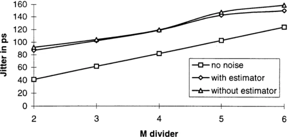
Figure 5.4 examines the effect of adding 100ps (picoseconds) of jitter to the reference clock at the VCO, while increasing the M and N dividers proportionally (keeping M/N constant). The three different signals represent the ideal case with no noise, noise added without the frequency estimator on, and noise added with the frequency estimator on. Please note that the LSB resolution for the next three sections is the same, so
comparisons between the effects of different types of additive jitter are valid.
160 140 120 100 80 60 40 20 0 2 3 4 5 M divider
The data shows that adding reference clock jitter has nearly the same effect on VCO jitter regardless of whether the estimator is on or not, which is not that surprising considering that the jitter is not accumulative. The fact that the estimator has a slightly better performance can be explained by the fact that once the loop has settled, the estimator acts to retard deviation from the ideal operating point.
In examining VCO jitter caused by reference clock jitter, the LSB resolution plays
an important role. The LSB resolution directly affects the loop gain, which in the
traditional sense directly affects the loop bandwidth. As the resolution increases, the loop's ability to track higher frequencies decrease, which means that the loop's ability to reject high frequency reference clock noise increases.
5.4
Jitter on the VCO
I OU 160 140 a, 120 ." 100 80 S60 40 20 0 2 3 4 5 6 M divider
Figure 5.5 examines the effect of adding 100ps of jitter to the VCO, while increasing the M and N dividers proportionally (keeping M/N constant). The three different signals represent the ideal case with no noise, noise added without the frequency estimator on, and noise added with the frequency estimator on. Notice once again that the estimator only makes the slightest improvement in noise rejection performance, which is not too surprising, remembering the non-accumulative nature of the jitter.
5.5
Wander on the VCO
In section 2.4, the following equation was explained: actual_period(n) = ideal_period(n)
+ jitter(n) -jitter(n-1) + wander(n). The effects of directly inserting jitter on the VCO were examined in the previous section. Therefore, since the wander term was zero, jitter was referenced to the ideal clock edge every period. However, if the wander term is nonzero, the effects of jitter become accumulative; past noise affects the current clock edge.
To illustrate this point, imagine a 100MHz clock. If this clock has zero-mean, 100ps jitter, after 100 cycles, the expected value of the time elapsed will be 1000 gs, while the standard deviation will be 100ps. However, if this clock has zero-mean, 100ps wander, after 100 cycles, the expected value of the time elapsed will still be 1000 gts, while the standard deviation will now be 1000ps. When adding two random processes, the means and variances add.
Figure 5.5 examines the effect of adding 100ps of wander to the VCO, while
increasing the M and N dividers proportionally (keeping M/N constant). The three different signals represent the ideal case with no noise, noise added without the frequency
estimator on, and noise added with the frequency estimator on. Notice that the estimator makes a significant improvement in noise rejection performance. This example better illustrates the retarding effect that the estimator has on the loop. With the accumulative noise, the fine tune word must deviate further from its ideal position to maintain phase lock. When phase reversal occurs, the estimator will bring the fine word back in closer to the ideal operating point.
1800 1600 1400 1200 1000 800 600 400 200 0 2 3 4 5 6 M divider
Figure 5.6. Wander added to the VCO
5.6 Tones on the Reference Clock
In the three previous sections, the effects the estimator has on the loop when noise is added have been examined. In each of these instances the ideal operating point for the fine word was constant, and the only reason the fine word changed at all (other than chatter) was to maintain phase lock at the phase detector. In the following two sections the effects of frequency tones will be examined.
Frequency tones affect the fine word in a different way than noise does. When noise enters the system, the fine word must adjust only to maintain phase lock at the phase detector, but the ideal operating location remains the same. When tones are present in the system, the fine word's ideal operating point must change to maintain both frequency and phase lock.
Figure 5.7. Digital phase-locked loop
From examining Figure 5.7, the closed-loop transfer function can be derived.
Y(s) 1 1 K ( +
s M
( + )z
[5.1]X(s) sM 1+ 1 K2 K- (s + z) s, s-+ KK, (s+ z)
Ns s N
From this transfer function we find that at lower frequencies, the response is a constant, and at higher frequencies, the response is a one-pole role off. The overall loop acts as a low-pass filter. From this reasoning, the loop will track low frequency tones on the reference clock, while it will reject high frequency tones. The following set of figures will demonstrate this effect. They show the tracking ability of the loop with and without the estimator at four different frequencies.
0.4 MHz Tone on reference clock I without etimator (11) : t(S) 40.2meg 4.mog 39."nm 162nwg 161meg 159mg Is5meg ret elk (WE) : t(S) von
Su O1u 15u 20u 25u 30u 35u 40u 45u
t(s)
Figure 5.8. 0.4 MHz Tone on reference clock without estimator
0.4 MHz Tone on reference clock I with estimator
(Hk) : t(s) 40.3meg ref clk .me/ \ -/ \ \ i 40om.g / /
/
39.ameg (Hz) : ts) I62meg Isiewg Isorneg 15&r"Su 10u lSu 20u 25u 30u 35u 40u 45u S0u
Figure 5.9. 0.4 MHz Tone on reference clock with estimator
vco / N / \/\ I'/ / i/ \ \ - •.%,.-....,/ N._._
0.8 MHz Tone on reference clock I without estimator (Hz) : t(s) ref clk 40.2mg // 39.8me9 (Hzt) : t(s) 162mag 161meg l 60m~g 159meg 158meo VCo
4u 6u bu IOu 12u 14u 16u 18u 20u 22u 24u 26u 28u 30u 32u 34u
t(s)
Figure 5.10. 0.8 MHz Tone on reference clock without estimator
0.8 MHz Tone on reference clock I with estimator
(Hz) :t(s) ref lk 40.2meg 40meg 39.8meg (Ft) : t(s) 162meg 161meg 16 meg 159meg VCO
4u Su Bu IOu 12u 14u 16u 18u 20u 22u 24u 26u 2u 30u
t(s)
Figure 5.11. 0.8 MHz Tone on reference clock with estimator
... f _i __,.'t.' g ,!" '4 i'
ii ... ii f! :::88
I I ~ ~~~~ I I I: I I I I i i I
E . j
K l
!l "l-';'"~i~ ";I . ili"T::-I t1IrBl,";
i ' ii rsi I: i i " J i i ,•'
i . i. ,, c !1 IfrFf ,":' t,!
inE I ji~l•i". f !•'L ; !i'-17i ·-- i •I.•
i'i•i~ifT:iii~ i t ! !.i i',:,[,•i f•.it
I I I I I I I I 1 I I I I I
1.6 MHz Tone on reference clock / without esimator
(1) : (s)
ref clk
(k) : t()
vo.
12u 14u 16u 18u 20u 22u 24u 26u 25u
t(s)
Figure 5.12. 1.6 MHz Tone on the reference clock without estimator
1.6 MHz Tone on eference clock/with estimator
I- .-. /"
f\
i7!"•
I i \ \ i \ , i \ I \ / i i i 1 I i \ i \ i I \ / \ \ I \ i \ \ ' i \ ! \ \.Y "v -••\! i,. ref clk (t) t(S) vea4u 6u Wu O1u 12u 14u 16u 1Bu 20u 22u 24u
Figure 5.13. 1.6 MHz Tone on the reference clock with estimator()
Figure 5.13. 1.6 MHz Tone on the reference clock with estimator
' / / /h \ / , I \ i / \ / I II \ 'i I I \ / i \ ' \ i \ l /
\
I \ i i\ l''\r / t I\ • •i\ ' 40.2meg 40omeg 39.smeg lianmeg 1659meg 15"me .J I. : -I ..'
!
r'!:" --' i '-" ;-" 7 - 7 r . . .., !....
i, ..-
r-
!.
i,
L.. ,. i--,f i.. I I I I. j [ .Ii 40.2meg 40meg 39.meg 162meg 161meg 160meg 159meg ls58ameg U;U '-,Fi
"i
I I I I I I I·
I I II
isamKeo&2 MHz Tone on fertmnce clock / without estimator 40d.2m* 40mog 39Smeg 162mwg 161meg 1someg 15"m.g 40.2meg domeg 162meg 161meg 160meg 159meg 150meg (HO) : ts) ref elk
7u au 9u lOu 11u 12u 13u 14u 15u 16u 17u 1su 19u 20u 21u
t()
Figure 5.14. 3.2 MHz Tone on reference clock without estimator
3.2 MHz Tone on efmrence clock I with estimator
(Ht) : t() ref clk
(i-) :s)
3u 4u 5u 6u 7u bu Ou IOu 11u 12u 13u 14u 15u 16u 17u
Figure 5.15. 3.2 MHz Tone on reference clock with estimator)
Figure 5.15. 3.2 MHz Tone on reference clock with estimator
! \ / \ i \ I ! i \ • \ /
/
\ \ \ i w / i/ I i I I i I i ii iI S I i / i ,, , \I i, \/'
~\ \I\',,,
, r , '',,
\ i \ '\./
"•.
P, -i * -- , ,,--[ .. - - . ',, ., ,--' .i j'i , HJ L. ~ L "-": , ..-. , -,L "-i ,F " "] -' • " / ,i.., :q ,,i ! i :.... I t \ ft t\ I I I' i ii \ \ 7 I/ \\ i ,i I ' \ i , I \i\ i \ ! i i i \ f \ i i ' i i , , I / I *i i \ ' \ \ ,I \ Ii i · I i \ .1 Bi .'j I :; ,,•r ," -- i - i; ,• r ' " : I: F -,' F_ - r "i I-- "I r " " rIl- i: ,. - r--- - r--I •' _.-. .., I j._ L, i i i; .. i i L_..iI "ii
-•
i
.
-j"
I I I I I I I I I I I 1 I I (Ht) : t() voo - · · · ·The preceding figures show that the loop performs equally as well with or without the estimator. When frequency tones appear on the reference clock, the VCO is supposed to track them at lower frequencies, and reject them at higher frequencies, which it does. The VCO frequency changes directly as the fine tuning word changes.
5.7 Tones on the VCO
When frequency tones appear directly on the VCO, a different scenario happens. In this case the VCO should remain constant while the fine tuning word changes. An example will help demonstrate this idea. Imagine the power supply having a ripple on it. When the power supply increases, the frequency will increase even though the control word remains the same. In fact, the fine control word must decrease in order to offset this increase in frequency.
The problem with this happening in this loop is that the estimator retards deviation from the ideal operating point. However, in this case the ideal operating point is changing. It seems conceivable that the estimator may have the wrong impact, and that it will hamper the fine word from changing in the proper direction, which is not good.
It seems plausible that some critical frequencies exist such that the fine word is just able to keep up with the frequency tone. However, when a phase reversal occurs, the
fine word will jump back towards the average fine word, causing extra phase error. The following four figures show the effects of the estimator at two different frequencies. The first set of figures show that the estimator has no appreciable affect. The second set of figures show how the estimator can negatively affect the loop.
0.2 MHz Tone on VCO without estimator
(Hz : t(s)
10u 20u 30u 40u 50u SOu 70u O0u 90u
vco hreq 161meg 160.Smeg 1someg 1R.Smeg 159meg 0.11 0.05 vco phase 100u
Figure 5.16. 0.2 MHz Tone on the VCO without estimator
0.2 MHz Tone on VCO with estimator
(Hz) : t(s) 161meg vco freq 160mog 159mneg 0.1 0.05 -0.0 04.05 (cycles) : t(s) veo phase
10u 20u 30u 40u 50u IOu 70u 8Ou 90u lOOu
i(s)
Figure 5.16. 0.2 MHz Tone on the VCO with estimator
-" -0.0 -0.05 0.1 lilll;liid ... BdldiI ir: ISuii ' ~ ''~PFi$lllTI LA ' + , i, , , iA t , " ll!• "
V
I
,.,,
4
i i ~~iTiOiL
'I
r I I r I I I I (cycles) : t(a) " I0.4 MHz Tone on VCO without estimator
i1i
~il'jVllla
i
J
¶11
lijl
10u 20u 30u 40u 50u 60u 70u 8Ou 90u
t(s)
Figure 5.17. 0.4 MHz Tone on the VCO without estimator
0.4 MHz Tone on VCO with estimator
O1u 20u 30u 40u 50u 60u 70u bOu 90u
t(s)
Figure 5.19. 0.4 MHz Tone on the VCO with estimator 161meg 160.5meg v 160meg 159meg (Hz) : t(s) vco freq (cycles) : ts) vco phase 0.1 0.05 0.0 -0.05 -0.1
S
' N ii
'
1
"i
'
'
Yii
ii 162meg 161meg g 160meg 159meg osameg 1.0 0.5 S 0.0 -0.5 (Hz) : t(s) vco freq (cycles) :t(s) vco phase r , .M~ P. ! !" A I I i YI r: i I ve V prol t ýWvfm A A a A, V -I A 100u ---1.0.U!-Chapter 6
Conclusions
In the previous chapter, the algorithm underwent a complete characterization examining
its performance under realistic conditions. The frequency estimator provides
significantly faster locking times, as seen in Figure 6.1. The settling time of the loop with the estimator is directly proportional to original error and indirectly proportional to LSB resolution.
Non-accumulative jitter is rejected almost equally with or without the estimator functioning. Accumulative jitter, or wander, is rejected significantly more in the loop with the estimator than without. The estimator retards deviation from the ideal fine tuning word, which is why it rejects noise better.
Both loops act as a low-pass filter to frequency tones on the reference clock. The major fault of this adaptation is discovered when examining responses to frequency tones on the VCO. At some frequencies the estimator will actually take the fine tuning word further away from the correct location.
(H) :t(S) 162meg -ofreq s ii 15I" (0b) : S) 162meg ls1meg 1589m•g 1a8meg
0.0 5u IOu 15u 20u 25u 30u 35u 40u 45u SOu 55u i Ou
t(s)
Figure 6.1. Locking times with and without the frequency estimator
Another feature in the digital PLL is the phase detector. Not being able to
quantify phase error does have its drawbacks, but it also has its benefits. The loop is desensitized to noise quantity. Regardless of whether the VCO is 10ps or 200ps fast, the decision from the phase detector is the same.
This algorithm could truly prove to be useful in the digital domain, but it may also have uses in the analog realm. Replace the two fine tuning control words with two capacitors. When a phase reversal occurs, instead of taking the midpoint of two digital
words, take the average of the two capacitors.
The frequency estimator adaptation to the acquisition algorithm is quick and simple, and it could prove to useful for a variety of applications.