HAL Id: tel-00110543
https://tel.archives-ouvertes.fr/tel-00110543
Submitted on 30 Oct 2006HAL is a multi-disciplinary open access archive for the deposit and dissemination of sci-entific research documents, whether they are pub-lished or not. The documents may come from teaching and research institutions in France or abroad, or from public or private research centers.
L’archive ouverte pluridisciplinaire HAL, est destinée au dépôt et à la diffusion de documents scientifiques de niveau recherche, publiés ou non, émanant des établissements d’enseignement et de recherche français ou étrangers, des laboratoires publics ou privés.
Theoretical study of the Kondo effect in the quantum
dots
Pavel Vitushinsky
To cite this version:
Pavel Vitushinsky. Theoretical study of the Kondo effect in the quantum dots. Physics [physics]. Université Joseph-Fourier - Grenoble I, 2005. English. �tel-00110543�
TH`
ESE
pr´esent´ee par
Pavel Vitushinsky
pour obtenir le grade de
Docteur de
l’Universit´e Joseph Fourier - Grenoble 1
Sp´ecialit´e : Physique
Etude th´
eorique de l’effet Kondo dans les
boˆıtes quantiques
Soutenue le 3 Novembre 2005 devant la Commission d’Examen :
M. Gilles Montambaux Rapporteur
M. Peter W¨olfle Rapporteur
M. Frank Hekking Examinateur
M. Philippe Nozi`eres Pr´esident
Mme. Mireille Lavagna Directrice de th`ese
M. Andr´es Jerez Codirecteur de th`ese
M´emoire Pr´epar´e au sein du Service de Physique Statistique,
Magn´etisme et Supraconductivit´e, DRFMC, CEA Grenoble
Contents
Remerciements
7
1 General introduction 9
1.1 Kondo effect . . . 11
1.1.1 Metals with impurities . . . 11
1.1.2 Scattering by impurities . . . 12
1.1.3 Kondo effect at low temperatures . . . 15
1.1.3.a Perturbation expansion . . . 15
1.1.3.b Scaling . . . 15
1.1.3.c Numerical renormalization group approaches . . . 16
1.1.3.d Local Fermi liquid . . . 17
1.1.3.e Bethe-Ansatz . . . 17
1.1.3.f Large-N approach . . . 17
1.1.4 Universality and crossover . . . 18
1.1.5 Phase shift . . . 18
1.2 Measuring the electron transmission phase . . . 19
1.2.1 Quantum dots . . . 19
1.2.2 Transport properties of the quantum dots . . . 21
1.2.2.a Coulomb Blockade . . . 21
1.2.2.b Kondo effect in quantum dots . . . 22
1.2.3 Two-terminal Interferometers. Experiment of Yacoby et al. Phase locking. . . 23
1.2.4 Open interferometers . . . 28
1.2.4.a Experiment of Schuster. Coulomb blockade regime. . . . 28
1.2.4.b Experiment of Heiblum. Kondo correlation and unitary limit regimes. . . 30
1.2.5 Theoretical works . . . 34
1.2.5.a Phase shift . . . 34
1.2.5.b Phase lapses . . . 35
2 Theoretical analysis of the transmission phase shift of a quantum dot at zero temperature in the presence of Kondo correlations 37 2.1 Introduction . . . 39
2.2 Scattering Phase Shift . . . 39
4 CONTENTS
2.2.2 Scattering theory for the Anderson model . . . 41
2.2.2.a S-matrix . . . 41
2.2.2.b The Friedel sum rule . . . 42
2.2.2.c The partial Friedel sum rule . . . 44
2.2.2.d Levinson’s theorem . . . 45
2.2.3 Landauer conductance and Aharonov-Bohm effect . . . 48
2.2.3.a Landauer approach . . . 48
2.2.3.b Aharonov-Bohm effect in an open interferometer . . . . 49
2.2.3.c Experimental check of the dependence of the conduc-tance with the phase shift . . . 50
2.2.4 Scattering phase shift . . . 52
2.2.4.a Diagonalization of the hamiltonian of the Anderson model with two reservoirs . . . 52
2.2.4.b Solution of the Anderson model . . . 53
2.3 Conclusion . . . 58
3 Phase Lapses 63 3.1 Introduction . . . 65
3.2 Phase lapse at T = 0 in the unitary limit and Kondo correlation regimes 65 3.2.1 Magnetic and non-magnetic regimes. Phase diagram at T = 0 . . 65
3.2.2 Net current through an Aharonov-Bohm ring . . . 66
3.2.2.a Unitary limit regime . . . 67
3.2.2.b Kondo correlation regime . . . 68
3.2.3 Dependence of the source-drain current with the transmission am-plitude of the reference arm tref . . . 70
3.3 Conductance evolution in the low-temperature (T ≪ TK) and high-temperature (T ≫ TK) regimes . . . 71
3.3.1 Phase diagram at finite T . . . 71
3.3.1.a T ≪ TK . . . 71
3.3.1.b T ≥ TK . . . 73
3.3.1.c T ≫ Γ . . . 75
3.3.1.d Experimental situation . . . 75
3.4 Ring current in the Coulomb blockade regime . . . 77
3.5 Conclusions . . . 77
4 Transmission phase shift at finite temperature in the out of equilibrium situation 79 4.1 Introduction . . . 81
4.1.0.e Quantum dots vs impurity atoms . . . 81
4.1.0.f Nonequilibrium . . . 81
4.1.0.g Anderson model . . . 82
4.1.0.h Calculation of the current . . . 83
4.1.0.i Calculation of the phase . . . 83
CONTENTS 5
4.2.1 Large-N expansion . . . 86
4.2.2 NCA . . . 88
4.3 Slave bosons . . . 90
4.4 Keldysh formalism . . . 92
4.5 NCA for the Anderson model in the slave-boson representation . . . 100
4.5.1 Application to the out-of-equilibrium regime . . . 100
4.6 Numerical solution of the NCA equations . . . 109
4.7 Transmission phase shift of a quantum dot out of equilibrium . . . 113
4.7.1 Phase shift . . . 113
4.7.2 Modelling . . . 118
4.7.3 Results . . . 118
4.7.4 Results for the occupation number . . . 119
4.7.5 Results for the transmission phase shift . . . 120
4.7.5.a Effect of the temperature at equilibrium . . . 120
4.7.5.b Asymptotic behavior . . . 123
4.7.5.c Intermediate regime . . . 125
4.7.5.d Large bias voltage regime . . . 125
4.7.6 Comparison with experiments . . . 127
4.7.7 Conclusions . . . 128
4.7.7.a What is good? . . . 128
4.7.7.b What is bad? . . . 129
General conclusion
130
List of figures
132
6 CONTENTS
Remerciements
J’adresse en premier lieu mes profonds remerciements à Mireille Lavagna pour m’avoir accueilli dans le cadre d’un stage pré-doctoral et pour m’avoir proposé ensuite un projet de thèse sous son encadrement. Je la remercie pour sa participation active au déroulement de la thèse, pour ses conseils, ses encouragements, sa disponibilité permanente, sa patience, pour m’avoir donné la possibilité de bénéficier de ses compétences et de m’avoir éclairé sur les subtilités relatives à la théorie de la matière condensée.
Je remercie Andrés Jerez, le co-directeur de ma thèse, pour les nombreuses discussions, ses conseils, son aide, sa contribution au projet de thèse, pour m’avoir fait bénéficier de sa compréhension des phénomènes complexes et des méthodes adoptées à la théorie de la matière condensée.
Je remercie Peter Woelfle et Gilles Montambaux pour avoir accepté une lourde charge en étant rapporteurs du manuscrit, ainsi que pour les commentaires et suggestions qu’ils ont apportés.
J’exprime ma profonde reconnaissance au professeur Philippe Nozières, qui a accepté de lire mon manuscrit et je le remercie pour l’honneur qu’il m’a fait en présidant le jury chargé d’examiner cette thèse.
Je remercie Frank Hekking pour avoir accepté d’examiner ma thèse, pour son soutien et pour sa contribution à ma formation, spécialement dans le domaine de la physique mésoscopique. J’exprime ma reconnaissance à Louis Jansen, chef de SPSMS, pour son soutien tout au long de mon projet de thèse, pour sa disponibilité permanente qui a permis que mon séjour dans son laboratoire se passe dans les meilleures conditions.
Je remercie Vladimir Mineev, chef du Groupe Théorie au SPSMS, pour l’intérêt qu’il a exprimé à mon travail, ainsi que pour les nombreuses discussions et suggestions.
Je suis très sincèrement reconnaissant à Stephan Roche, Jacques Villain, Jacques
Schwiezer, Michel Bonnet, membres du SPSMS, qui ont toujours manifesté une grande
curiosité à mon travail, pour leurs conseils sur le fond ainsi que sur la forme de mes exposés scientifiques. Je les remercie pour la chaleur de leur accueil qui m’a permis de m’adapter à la société française, ce qui a rendu mon travail durant la thèse plus efficace.
Je tiens à exprimer ma gratitude à Ramon Aguado pour les discussions que nous avons eues et ses conseils qui m’ont aidé à bien avancer la partie de la thèse reliée au déphasage hors équilibre à température finie.
Je remercie Denis Feinberg, Pascal Simon, Laurent Saminadayar, Christopher Bauerle,
Karyn Le Hur pour leur intérêt à mon travail, les nombreuses discussions et suggestions.
J’ai aussi profité de nombreuses discussions avec Thierry Champel, Damien Bensimon, Vu
Hung Dao, François Triozon, étudiants et post-docs dans le Groupe Théorie du SPSMS.
Qu’ils en soient remerciés.
Chapter 1
10 Chapter 1. General introduction
1.1 Kondo effect 11
1.1
Kondo effect
1.1.1
Metals with impurities
Conduction electrons in normal metals behave as weakly coupled (interacting) quasi-particles. A good description is provided by the theory of Fermi liquid developed by L. Landau. Considering normal metals containing impurities it was shown that in the framework of the Fermi liquid description the electric resistivity of the metal sample drops when temperature decreases. The resistance starts saturating as temperature is lowered below about 10 K due to static defects in the material. Generally the temper-ature dependence of the resistance is given by
ρ(T ) = ρ0
¡
1 + aT2¢ (1.1)
where ρ0 is the zero-temperature conductance. ρ0 comes essentially from the scattering
of conduction electrons by static impurities while the quadratic term is due to other types of scattering processes, like the scattering of electrons by electrons or by lattice vibrations, which becomes weaker and weaker as temperature is lowered. The value of the low-temperature resistance depends on the number of defects in the metallic sample but the character of the temperature dependence remains the same. Some metals, however, can have their electric resistance dropped at low temperature and become superconducting. In our work we will not consider the case of superconducting metals and focus instead on normal metals.
However the low-temperature behavior changes drastically when magnetic atoms are added. The electronic shells of these atoms correspond to only partially filled outer d or f shells and may have nonzero net magnetic moment, such as for example cobalt,
27Co, iron, 26Fe, or manganese 25Mn. The resistance of this alloys first decreases and
then increases as temperature is lowered. The origin of this increase of the resistance has been the subject of many theoretical studies. It was established experimentally that the minimum appears when and only when the alloy contains magnetic impurities, the resistance minimum is thus a universal phenomenon of dilute magnetic alloys. Another important point was clarified later on through the measurements of the resistance of diluted alloys with an impurity concentration less than 0.1 at.%. This result showed that the residual resistance is proportional to the impurity concentration and increases as temperature is lowered. Thus it was established that the phenomenon is a single impurity effect rather than due to the interaction between impurities.
To summarize, any theoretical analysis is confronted with three main obstacles. The first one is the resistance increase when temperature is lowered. Any source of electron scattering should vanish as temperature is lowered and the scattering probability should decrease in metals except in very special cases. The second one is the fact that residual resistance is not a constant but varies at very low temperatures. The origin of the corresponding energy scale was not clear. The third difficulty is the universality of the phenomenon. A large number of alloys were tested experimentally and all lead to the similar results. From the latter reason one expect the model to be relatively simple and very general, universal for all magnetic alloys. In fact, the standard model introduced
12 Chapter 1. General introduction
Figure 1.1: Temperature dependence of the resistivity of pure metal (Cu) and dilute magnetic alloy [1].
to describe localized moments in a metal is the so-called s–d model, which was treated extensively and found to give a monotonic decrease of the resistance below the Neel temperature [2, 3].
1.1.2
Scattering by impurities
In the case of the scattering by impurities which do not own any internal degree of freedom, as for example for the scattering by a potential
X
i
v(r − Ri) (1.2)
the scattering can be analyzed in terms of a one-particle problem since each electron sees the same scattering potential. The situation is very different when the scatterer owns internal degrees of freedom as, for example, spin or orbital degeneracy. After each scattering event the ground state of the scatterer and therefore the potential seen by the electrons may change. Correlations between electrons are introduced and the problem, thus, is no longer a one-particle but rather a many-body problem. In addition to the potential expressed in Eq.1.2 the interaction energy of an electron with a magnetic atom contains a coupling term between the spins σ and S of the conduction electron and the impurity. It can be written in the framework of the s-d model
Vs = −(J/n)
X
i
1.1 Kondo effect 13
Figure 1.2: Temperature dependence of the resistivity for different concentrations of impurity atoms - comparison between experiment (circles) and theory (curves) [4].
The coefficient J has the dimension of energy. J is several times lower than the electron energies, which are of the order of µ, whereas the usual spin-independent interaction of an electron with an impurity atom is of the order of µ. The latter interactions do not interfere in the scattering probability and one may consider them separately.
The spin part of the interaction gives a contribution of the order of J2S2/µ2 to
the scattering probability with respect to the usual interaction. It seems that this is a small effect which can be neglected. It is known that usually the interaction is not weak and one has to take into account higher order terms in the calculation of the scattering probability. However, more detailed calculations in this case show that the result remains similar.
The situation is rather different for the spin-dependent part of the interaction. Al-though it is smaller than the spinless part there is nevertheless a significant difference. The importance of the higher order corrections was first shown by Jun Kondo [4]. The point is that the interaction described in Eq.1.3 corresponds to the physical process in which the electron spin can flip together with a simultaneous spin-flip of the impurity. When an electron is scattered off an usual atom its spin keeps its orientation. The correction appears to be dependent on the energy of electron leading to a temperature dependence of the resistance. Jun Kondo showed that the minimum of the resistance is due to the process of spin exchange between free electrons and the localized impurity.
14 Chapter 1. General introduction
The scattering probability calculated at the third order in J is proportional to log T as a result of the non-commutativity of the spin operators. The sign of this log T term depends on the sign of J. The scattering amplitude decreases for positive values of J and increases if J < 0. This effect has a physical explanation. If J > 0, then the interaction is of ferromagnetic type and favors the parallel alignment of spins σ and S. In this case the spin-flip scattering is suppressed and the scattering amplitude (and thus the resistance) decreases with temperature. Conversely, for negative J the interaction is antiferromagnetic and the processes with a flip of electron spins are now possible. This leads to an increase of the resistance when the temperature is lowered.
At high temperatures the main contribution to the resistance is due to electron-phonon scattering. The thermal dependence of the resistance is given by
ρ = ρv + cma ln
µ T + bT
5 (1.4)
where cm is the atomic concentration of magnetic impurities, a and b are constants and
ρv is the contribution to the resistivity brought by the potential scattering. The latter
term, resulting from the electron-phonon interaction, increases with temperature. The interplay between the two last contributions gives rise to a minimum in the resistance as a function of temperature at Tmin given by
Tmin =
hcma
5b i1/5
(1.5) As can be seen Tmin is proportional to c
1/5
m and hence weakly depends on cm. J. Kondo
have also shown that the scattering cross-section obtained by perturbation expansion diverges as a given temperature. The temperature at which the logarithmic term in the perturbation expansion becomes large is given by
TK ∼ (Jµ)1/2exp · − n |J| ν(µ) ¸ (1.6) where ν(µ) is the electron density of states at the Fermi level. This temperature is called the Kondo temperature.
The physical phenomena related to this process are known as the Kondo effect whereas the class of theoretical models proposed to describe this effect are called -the Kondo models. Since -then -the properties of Kondo systems have intensively been studied. A complete and detailed overview of this question can be found in the book of A.Hewson [5].
Earlier, in the late 50s the concept of ”virtual bound state” was introduced by J.Friedel. These are states which are almost localized due to the resonant scattering by the impurity. This idea was developed later on by P.W. Anderson (1963) in a paper in which he proposed the ”Anderson model” [6]. This model has then played a very important role. The model contains, in addition to the resonance at the impurity site, a strong on-site interaction arising from the Coulomb repulsion between impurity electrons. This interaction is responsible for the formation of a localized magnetic moment at the impurity site. For the calculation of the resistance, Kondo assumed
1.1 Kondo effect 15
(it was the intrinsic property of the model considered) a local magnetic moment to be associated with the spin S. The Anderson model is more general than the s-d model – the latter can be deduced from the former in a given limit. The transformation mapping the Anderson Hamiltonian to the s–d (or Kondo) hamiltonian can be performed using unitary operators. It is known as the Schrieffer-Wolff (canonical) transformation (1966).
1.1.3
Kondo effect at low temperatures
1.1.3.a Perturbation expansion
Perturbation theory expansion in J leads to unphysical predictions such as a divergence of the resistivity at T = 0. The summation of the infinite series of leading order logarithmically divergent terms was performed by A.A.Abrikosov [7]. His result extends the calculation of J. Kondo. The expression that he gets for the resistivity leads to reliable results for the ferromagnetic case J > 0. For the antiferromagnetic case, J < 0, the resistance becomes infinite at the Kondo temperature TK. The divergence of the
resistance results from the formation of a singlet state (Kondo singlet) between the spins of the conduction electrons and the spin of the impurity [8]. In other words, it corresponds to a complete screening of the impurity by the conduction electrons surrounding it, forming what is called the ”Kondo cloud”.
Perturbation theory provides a good description of the magnetic impurity systems for T ≫ TK but the expansion breaks down at T ≪ TK. The perturbation expansion
predicts a log T -form for the resistance at low temperatures while experimental studies show that both thermodynamic and transport quantities give power laws in T . The resistivity, for example, deviates from its T = 0 value by T2 terms. Non-perturbative
techniques are required to investigate the low-T regime. 1.1.3.b Scaling
In the late 60s Anderson and coworkers introduced a new theoretical framework based on the ideas of scaling [9, 10]. They proposed to perturbatively eliminate higher-order excitations allowing then to derive an effective model valid at low energy scales. The width of the conduction band in this method is gradually reduced so that finally only low-energy excitations are allowed. This procedure generates a set of effective models, each one characterized by its own coupling J. Additional couplings are also generated in this procedure but most of them are ”small” and can be neglected. Thus the coupling J varies with the width of the conduction band: J = J(D). The scaling approach leads to the concept of the existence of fixed point when J(D) becomes scaling-invariant. The system is then described by the fixed point corresponding to the value of J∗ = J(D′)
where D′ is defined from
· d J(D) dD ¸ D=D′ = 0. (1.7)
The scaling approach leads to an increase of the effective coupling strength between the spins of conduction electron and of the impurity when D decreases, allowing one
16 Chapter 1. General introduction
Figure 1.3: Formation of the spin singlet complex at low temperatures. Magnetic impu-rity virtually traps one conduction electron in order to compensate its magnetic moment.
to describe the low temperature behavior of the system. The perturbation approach breaks down when J becomes too large but Anderson assumed that the approach is still valid at very low temperatures, T → 0. If the scaling is pursued further, the coupling J increases to infinity as D is reduced. Such a scaling behavior implies the formation of a ground state with an infinite coupling in which the impurity is bound to the conduction electrons in a spin singlet state. The behavior at low temperatures is similar to that of a non-magnetic impurity, Fig.1.3.
An outstanding result of the scaling approach is that each set of effective models is characterized by a single energy scale, TK, which is a scaling invariant. Systems with
different values of the parameters J and D but with the same TK = TK(J, D) exhibit
the same low energy behavior. Hence, for example, the low-temperature dependence of the resistance is given by
ρ(T ) = F µ T TK ¶ (1.8) where F (x) is a universal function.
1.1.3.c Numerical renormalization group approaches
An important contribution was made by K.G.Wilson. He developed a non-perturbative method - the numerical renormalization group approach (NRG). Wilson combined the renormalization group ideas coming from field theory with scaling arguments derived from condensed matter physics. He was then able to confirm Anderson’s hypotheses [11, 12]. Wilson, after solving numerous technical problems, obtained the solution for the ground state and the low-energy excitations of the s-d (Kondo) model with impurity spin S = 12. One of the more spectacular results concerns the value of the ratio χ/γ (where χ is the magnetic susceptibility and γ is the low temperature specific heat coefficient) named since then as the Wilson ratio. The value of this ratio was found to be twice the value of non-interacting electrons.
1.1 Kondo effect 17
1.1.3.d Local Fermi liquid
P. Nozi`eres gave an interpretation of Wilson’s low temperature results in terms of a Landau Fermi liquid theory [13]. At low temperatures T ≪ TK the impurity spin is
completely screened, i.e. the total spin of the composite formed by the impurity and the screening conduction electrons is zero. This composite induces polarizability effects. One electron polarizes the composite and then this polarized composite acts on another electron. This mechanism provides an indirect interaction between conduction electrons located in the vicinity of the composite. Therefore, an interaction is induced between conduction electrons leading to the formation of a local Fermi liquid. The problem of the magnetic impurity coupled to a gas of non-interacting electrons is then replaced by that of quasiparticles interacting through the non-magnetic composite. The latter interaction is local, acting at the site of the impurity hence the name of ”local Fermi liquid”.
Within this description Nozi`eres gave a simple derivation of the χ/γ result as well as an exact calculation of the T2 coefficient for the resistivity. In a phenomenological
way Nozi`eres incorporated in his Fermi liquid description the values of the parameters extracted from Wilson’s calculations in the Fermi liquid description.
1.1.3.e Bethe-Ansatz
In the early 80s N. Andrei [14, 15] and independently P.B. Wiegmann [16, 17] showed that the Kondo model is an integrable model and found the exact solution using the Bethe-Ansatz. They derived a set of integral equations the resolution of which allows them to derive the temperature behavior of thermodynamic quantities over the whole range of temperatures. This result confirmed Wilson’s calculations. More importantly the method proved to be generalizable to other models like, for example, Anderson model. Most of the models proposed for the description of dilute magnetic alloys were proved to be integrable. Let us remind that the Bethe ansatz method, originally pro-posed to solve the 1D Heisenberg model, was used to solve other one-dimensional models. The condition behind is that only the electronic waves of s-wave symmetry contribute to the scattering off the Kondo impurity (s-wave scattering). Then the problem can be reduced to an effective 1D problem.
1.1.3.f Large-N approach
In order to discuss the results obtained by various experimental techniques is physi-cal systems, such as photoemission and neutron scattering experiments, the dynamic response functions are required. These functions can not be calculated in the frame-work of the Bethe anzats. Many approximate techniques then were developed based on large-N approaches where N is the degeneracy of the localized states. In some physical systems the degeneracy of the localized state can be as large as N = 6 for Ce or N = 8 for Y b. Asymptotically this description gives the exact result in the limit N → ∞. At finite N , one needs to introduce 1/N (or (1/N )2) corrections. This is done by
18 Chapter 1. General introduction
variational or diagrammatic techniques. These methods were used to calculate the one electron density of states and the dynamic susceptibility. What was clearly shown was the formation of a very narrow many-body resonance in the density of states at the Fermi level in the Kondo regime (known as the Kondo resonance). This resonance is responsible for the anomalous low-temperature behavior of many physical quantities.
1.1.4
Universality and crossover
One of the most essential property of the Kondo effect is the universality. It was found that all physical quantities are universal functions of energy (T or H for example) renormalized by the Kondo temperature TK: T /TK, H/TK ... when the conduction
bandwidth D is the largest energy scale of the problem. This property implies that in a set of experimental systems corresponding to different values of parameters, the measured physical quantities exhibit the same (universal) behavior as a functions of renormalized variables T /TK or H/TK.
Therefore, the Kondo temperature is the only energy scale of the problem at low temperatures. This energy scale defines the range of applicability of the perturbation expansion. TK, is neither a property of the host metal nor of the impurity atoms
but is generated dynamically by the interaction between them. In the intermediate temperature regime, T ∼ TK, which separates the low-energy Kondo regime from the
high-temperature (perturbative) regime, the properties of the system change gradually around TK defining the crossover as a contrast to a phase transition.
1.1.5
Phase shift
Since the impurity is local each quasiparticle state in the electron system is characterized by a given phase shift, δ. All the physical properties of the model at zero temperature can be expressed in terms of this quantity. Thus the phase shift is one of the most fundamental quantity of the model allowing to describe the zero temperature behavior. In dilute magnetic alloys, i.e. for magnetic impurities imbedded in a bulk metal, the direct observation of the phase shift is out of scope.
As we will see later on the scattering phase can not be obtained from simple trans-port experiments where only conductance (or resistivity) is measured. Only indirect observation is possible. At very low temperatures the effective coupling between the spin of an impurity and the spin of conduction electrons becomes infinite. As a result the scattering crossection reaches its maximum value at T = 0 (this regime is often named as the unitary limit). The phase shift then is supposed to be equal to π2 in order to ensure the maximum of the resistivity. A direct measurement of the phase shift has become possible in quantum dots thanks to combined progress realized in nanofabrica-tion and quantum interferometry. The results obtained in a series of recent experiments do not confirm the expected value. These results gave us the motivation for the study undertaken in this thesis.
We will present in the next section the different experiments carried out to measure the phase shift.
1.2 Measuring the electron transmission phase 19
1.2
Measuring the electron transmission phase
Landauer showed [18, 19, 20] that a tunnelling event can be considered as a scattering experiment. In the case of a single plane wave scattered by a center, the conductance is shown to be proportional to the square of the magnitude of the transmission ampli-tude of the scatterer. It is therefore obvious that the difference of phase between the incoming and outgoing electron waves can not be measured in a transport experiment. In coherent processes, the phase of the transmission amplitude plays a role and brings additional information which is not contained in conductance measurements. The phase can be determined by using Aharonov-Bohm effect which directly probes both the trans-mission amplitude and probability provided that transport is coherent. In general, the Aharonov-Bohm ring conductance shows oscillations as a function of a magnetic field penetrating its inner core, with a periodicity equal to one flux quantum h/e. One thus expects these oscillations to persist when a quantum dot is embedded to one of the arms of Aharonov-Bohm ring as soon as transmission through the quantum dot is coherent.
The idea and the practical implementation of devices for measuring the electron transmission phase through a quantum dot was developed in a series of ingenious experi-ments [21],[22] at the Weizmann Institute. The experiexperi-ments utilized an Aharonov–Bohm (AB) ring with a quantum dot embedded in one of its arms. The measurements of the electron phase revealed a number of unexpected results. The technique for measuring the electron phase and the main experimental results are described in this section.
1.2.1
Quantum dots
The interest in measuring the transmission phase resulting from the scattering off a quantum dot is due to certain similarities existing between real atoms and quantum dots in their electronic properties. A quantum dot can be viewed as a large atom [23, 24, 25, 26, 27, 28] the radius of which is of the order of a few hundreds of nm, containing up to a few hundreds of electrons. As it is dictated by quantum mechanics, particles confined in a finite-size box have a discrete energy spectrum with spacing proportional to (1/L)D where L is the characteristic size of the system and D its dimensionality.
The energy spectrum of the dot is constituted by single particle levels, each one being broadened due to tunnelling into and out of the quantum dot. Because of its small electric capacitance the addition of an extra electron into the quantum dot requires a relatively large energy, named as the charging energy e2/2C where C is the capacitance
of the dot. As a result the states corresponding to different values of occupation of the quantum dot, appear to be separated by a large energy gap (with the exception for the case of resonances - when the quantum dot is in a mixed state between |Ni and |N + 1i). Thus the total charge located in the dot is a well defined integer number. It may happen that the quantum dot is occupied by an odd number of electrons. This implies a non-zero total magnetic moment in the quantum dot. A quantum dot in this case behaves as a (atomic-type) magnetic impurity embedded in a host metal.
The quantum dots turn out to be tunable devices. The corresponding parameters, which are out of control in the case of magnetic impurities in bulk metals can now be
20 Chapter 1. General introduction
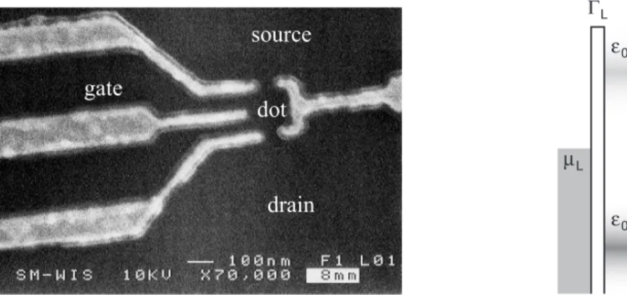
Figure 1.4: Left: Scanning electron microscope image of a typical quantum dot (top view). The black regions indicate the 2DEG, gray regions indicate the metal gates [29]. Right: Schematic representation of quantum a dot structure.
tuned experimentally, opening the way to systematic study of the underlying physics. A typical quantum dot is represented in Fig.1.4 (left). The experimental setup was realized on the top of a GaAs–AlGaAs heterostructure supporting a two-dimensional electron gas (2DEG). The quantum dot was designed by depositing metal gates on the surface of the heterostructure and subsequently biasing them negatively in order to deplete the electron gas underneath. The dot is connected to the source and the drain via quantum point contacts. A bias voltage, the difference in potential between the source and the drain, can be applied resulting in a current flow through the dot. The conductance of the dot can be adjusted by tuning the lateral gate voltage (upper and lower gates on the left side of Fig.1.4(Left)) which control the transparency of these quantum point contacts via the lateral gate voltages VgS and VgD. This set-up enables
a continuous variation of the dot’s resistance. A third gate (the central gate on the left side of Fig.1.4(Left)) controls the area and the electrostatic potential in the dot. The dot is about 100×100 nm in size. The quantum dot has usually a very small capacitance C corresponding to a large charging energy e2/2C - the energy which is necessary to
add (or remove) one electron in (from) the dot.
Quantum dots can be modelled as schematized in Fig.1.4 (right). The central region, which corresponds to the dot (see Fif.1.4 (left)), displays a discrete energy spectrum. It is coupled via tunnel barriers to the source and the drain which are modelled by Fermi seas. It is possible to make a one-to-one correspondence between the parameters of this model and the experimental parameters. The energy of the localized level in the dot, ε0, is equivalent to the gate voltage, VG. Further, the relation between them
is assumed to be linear. By tuning the gate voltage one adjusts the level position in the dot relatively to the chemical potentials in the leads. Once the dot contains N electrons it costs U to add another electron to the dot, where U = e2/2C is the charging
energy. The rates at which electrons enter and leave the dot, ΓL and ΓR, are controlled
experimentally by tuning the lateral gate voltages, VgS and VgD. The bias voltage, VSD,
controls the difference between the chemical potentials in the left and right reservoirs, i.e. VSD = e(µL− µR).
1.2 Measuring the electron transmission phase 21
Figure 1.5: (A) Conductance through the quantum dot as a function of gate voltage VG,
[30]. The quantum dot is either in a ”locked” (B) or an ”open” (C) regime.
1.2.2
Transport properties of the quantum dots
1.2.2.a Coulomb Blockade
When the Fermi energy in the leads, µ, lies within the gap between the topmost occupied, ε0, and the first empty, ε0+ U , energy levels the number of electrons in the dot is almost
fixed, Fig.1.5(B). Putting an additional electron into the dot costs an extra energy equal to the charging energy e2/2C where C is the capacitance of the device. When
temperature is low enough and the charging energy is large the probability of such an event becomes small and the electron transfer from one to another reservoir is strongly reduced. As a result the conductance through the quantum dot is almost zero [31]. The transport through the dot is said to be locked.
By tuning the gate voltage one can align the energy of the localized level, ε0, with
the Fermi energy in the leads, µ, Fig.1.5(C). In this case the electrostatic energies of the quantum dot with N or N + 1 electrons are equal. Such a degeneracy between different charge states of a quantum dot allows the electron of one reservoir to tunnel through the dot into the other reservoir. The charge transport is made possible leading to a finite conductance through the dot. The calculations show that the conductance through the quantum dot remaines finite in a narrow region of width Γ = ΓL+ ΓR around µ or or a
thermal window of width T , depending whether Γ or T is the large energy scale. Experimentally, when tuning continuously the gate voltage VG and measuring the
conductance of a quantum dot, one observes a series of high and narrow peaks separated by valleys of almost zero conductance, Fig.1.5(A). The resulting oscillatory dependence of the conductance G(VG) is the signature of the Coulomb Blockade effect. The dot
is then said to be in the Coulomb Blockade regime. The contrast between the con-ductance in the Coulomb blockade valleys and resonances becomes larger and larger as temperature is lowered. Conductance peaks correspond to values of the gate voltage VG for which the energy of one of the localized levels in the dot is close to the Fermi
energy in the leads. For all the other values of VG the conductance is very low. When
VG continuously increases and the conductance passes a resonance, it means that one
22 Chapter 1. General introduction
Figure 1.6: Conductance as a function of VG for different temperatures. T ranges from
15 mK (black trace) up to 800 mK (red trace) [32].
number of electrons in the dot. The gate voltage VG effectively controls the occupation
of the dot. Depending on the parity of the occupation in the dot, one can distinguish ”even” or ”odd” conductance valleys.
As temperature increases the probability for one electron to tunnel through the blockaded dot increases. The conductance in the valleys then increases with temperature in both the ”even” and ”odd” conductance valleys. The peaks becomes larger and of smaller height when temperature increases.
1.2.2.b Kondo effect in quantum dots
If an odd number of electrons occupies the dot, the total spin of the dot is necessarily non-zero. It has a minimum value of S = 12. This localized spin S, coupled to the source and the drain, mimics the behavior of a localized magnetic impurity in the host metal. As we will show later, these two systems are equivalent and many of Kondo phenomena can be expected to occur in quantum dots.
One of the most distinct features between quantum dot and magnetic impurity in metal is related to their different geometries. In real metals the magnetic impurities scatter the conduction electrons which strongly contributes to the resistance. In a quantum dot all the electrons have to travel through the scatterer, as there is no electrical path around it. In this case the onset of a new scattering mechanism due to the Kondo resonance contributes to the conductance. As the resistance in bulk metals in the Kondo regime, the conductance of the quantum dot at low temperatures depends only on the ratio T /TK, where TK is Kondo temperature.
1.2 Measuring the electron transmission phase 23
Figure 1.7: Conductance as a function of temperature for different values of gate voltage VG. Plotted as functions of T /TK all the curves show a universal behavior [32].
The conductance of a quantum dot as a function of the gate voltage was measured in the experiments of D.Goldhaber-Gordon et al. [32], Fig.1.6. For an even number of electrons, the conductance decreases as the temperature is lowered from 0.8 K to 15 mK. This behavior indicates that there is no Kondo effect when the number of electrons in the dot is even. In contrast, when the number of electrons is odd the conductance of the dot increases when the temperature is lowered. Moreover, at lowest temperatures the conductance approaches the quantum limit of conductance 2e2/h. In
terms of the scattering description of electronic transport, the quantum dot in the limit T = 0 becomes completely transparent, the probability of an electron to be transmitted from the source to the drain equals unity. The dot is said to be in the unitary limit (UL) regime. In the low temperature limit the conductance measured at different values of the gate voltage VG, i.e. different values of ε0, shows clearly different temperature
behavior. But plotted as a function of T /TK, all the curves lie on top of each other,
i.e. the experimental data exhibit universal behavior below TK. The three following
features — the asymmetry in the low-temperature behavior of the conductance between the Coulomb blockade valleys of different parity; the increase of the conductance in the ”odd” valleys reaching the unitary limit 2e2/h under some condition its universal
low-temperature behavior — constitute clear manifestations of the Kondo effect.
1.2.3
Two-terminal Interferometers. Experiment of Yacoby et
al. Phase locking.
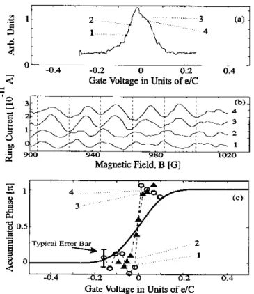
The first experiment addressing the electron phase through a quantum dot was realized by Yacoby et al. [21]. The experiment utilized a novel device (see Fig.1.8) to measure the phase evolution through the dot against a reference phase which is supposed to be fixed. The Aharonov-Bohm interferometer was composed of two arms forming the ring. The quantum dot was inserted in one arm of an Aharonov–Bohm ring. The basic idea
24 Chapter 1. General introduction
Figure 1.8: Electron micrograph of the Aharonov-Bohm interferometer used in the [21]. The black regions indicate the 2DEG, gray regions indicate the metal gates. Electrons flow between source and drain through the left or the right arm of the Aharonov–Bohm ring. The quantum dot is inserted in the left arm. The central metallic island is biased via an air bridge (B) [21].
is to extract the transmission phase through the quantum dot from the phase of the Aharonov–Bohm current collected at the drain. The dot was about 0.4µm × 0.5µm in size. A special lithographic process, invoking a metallic air bridge (B), enabled to contact the center metal gate that depleted the electrons underneath the ring’s center. Each of the arms of the Aharonov-Bohm ring supported a few conducting modes. The ring was connected to two external contacts, source (S) and drain (D), between which a small voltage was applied.
The elastic mean free path in the two–dimensional electron gas was estimated to be about 10 µm while the diameter of the Aharonov–Bohm ring was L ≈ 1 − 1.5 µm. The phase coherence length Lφ was larger than the ring’s circumference. The quantum dot
had a resistance of 1M Ω and a very small capacitance C ≈ 160 aF corresponding to the charging energy e2/2C ≈ 0.5 meV . The dot contained around 200 electrons. The bare
average single–particle level spacing was ∆ ≈ 40 µeV . The experiment was performed at a temperature around 100 mK corresponding to the thermal energy kT ≈ 9 µeV . The intrinsic width Γ of the Coulomb peaks was estimated from the conductance peak height to Γ ≈ 0.2 µeV . These scales imply that the quantum dot was in the Coulomb blockade regime, and that the transmission at each Coulomb peak resulted from resonant tunnelling through a single resonant level of the quantum dot.
The experiment [21] demonstrated for the first time that part of the tunnelling current through a quantum dot is coherent. The experimental evidence is presented in Fig.1.9. The figure shows the ring current as a function of the plunger voltage VP (also
often referred as the gate voltage, VG) for a fixed small source–drain voltage. The ring
1.2 Measuring the electron transmission phase 25
Figure 1.9: The ring current as a function of the plunger gate voltage. The large current of the reference (right) arm has been subtracted. The top left part shows the Aharonov– Bohm oscillations of the current as a function of magnetic field at fixed VP = Vm. In
the inset: oscillation contrast defined as the amplitude of the ring current oscillations vs. the average current through the dot [21].
VP–independent background current due to the right arm. The Coulomb blockade in
the dot manifest itself in a series of sharp conductance peaks in the ring current at fixed magnetic field. Fixing the voltage VP on the side of a current peak and sweeping the
magnetic field, one observes periodic current oscillations. The period of the oscillations corresponds to one flux quantum threading the area of the ring, in very good agreement with the expected period of Aharonov–Bohm oscillations, providing a direct indication that transport through the quantum dot has a coherent component. The oscillation contrast, defined as the peak–to–peak current over the average current, does not varies much and is in the range 0.2 to 0.4.
In a next step, the current oscillations were investigated at different values of the plunger voltage VP. A change in VP was expected to modify both the magnitude and the
phase of the transmission amplitude through the dot. The experiment was motivated by the idea that the change in the transmission phase would be directly reflected in a shift of the Aharonov–Bohm oscillations which, in turn, could be seen experimentally. This one–to–one correspondence is suggested by the following argument: suppose the ring and the leads support only one conducting channel. According to the Landauer formula, the zero–temperature current between the leads is proportional to the ring transmission coefficient |t(EF)|2 at the Fermi energy EF. For fully coherent transport,
t = tRexp(2πiΦ/Φ0) + tL, where tR and tL are the transmission amplitudes through
26 Chapter 1. General introduction
Figure 1.10: (a) A series of three Coulomb peaks and (b) the current oscillations mea-sured at the marked points A, B, and C. All oscillations are seen to be in phase. The large current of the reference (right) arm has been subtracted [21].
quantum. This leads to the interference term
2Re{tLt∗Rexp(−2πiΦ/Φ0)} = 2|tR||tL| cos(ξL− ξR− 2πΦ/Φ0), (1.9)
where ξR= arg(tR), ξL= arg(tL). Any shift in the phase ξL− ξR should thus be directly
reflected in a shift of the Aharonov–Bohm oscillations.
The above argument turned out to be incorrect. It neglects multiple reflections through the ring. The argument fails in particular for a two–terminal geometry, i.e. a ring connected to two external leads. It was realized just after the experiments were performed that Onsager relations valid for a two–terminal device restrict the phase of the Aharonov–Bohm oscillations to either 0 or π, spoiling the correspondence between the Aharonov–Bohm phase and the transmission phase through the quantum dot. This property is general for systems where current is conserved and time-reversal symmetry is satisfied [33]. Only abrupt jumps between the two allowed phase values are possible. Physically, this is a direct result of the interference between the different paths that traverse the ring. Nevertheless the idea of measuring the electron phase was later realized in the multiple–terminal device of Schuster et al. [22].
Figure 1.10 shows the ring current and the Aharonov–Bohm oscillations measured at three successive peaks. The oscillations at similar points (A, B, and C in the figure) have the same Aharonov–Bohm phase. This repetition of the phase was found within the whole sequence of Coulomb peaks (comprising 12 peaks) investigated in the experiment. The evolution of the Aharonov–Bohm phase along a single Coulomb peak is displayed in Fig. 1.11. Four different interference patterns taken at the points 1, 2, 3, and 4 specified in Fig. 1.11(a) are shown in Fig. 1.11(b). The Aharonov–Bohm phase of the patterns jumps by π as one sweeps through the peak. The jump happens abruptly between the points 2 and 3. This can be seen in Fig. 1.11(c) which summarizes the phase
1.2 Measuring the electron transmission phase 27
Figure 1.11: Evolution of the Aharonov–Bohm phase through a current peak. (a) Current as a function of gate voltage (or plunger voltage VP ≡ VG) at a current peak.
(b) A series of interference patterns taken at the points specified in (a). Note the phase jump between patterns 2 and 3. (c) Phase measured at two peaks (circles and triangles). The broken line is guide to the eye. The expected behavior of the quantum dot transmission phase in a 1D resonant tunneling model is shown by the solid line [21].
28 Chapter 1. General introduction
measurements along a Coulomb peak. The sharp jump in the measured Aharonov– Bohm phase is in contradiction with the expected phase evolution of the transmission amplitude assuming resonant tunnelling through a single level of the quantum dot. The latter phase increases smoothly on the scale of the peak width (which is of order kT ). This disagreement arises from the fact that closed two-terminal Aharonov-Bohm ring can not be described by the ”two-slit” result expressed in Eq.1.9 and one needs to take multiple reflections through the ring into account in order to recover the correct result.
1.2.4
Open interferometers
1.2.4.a Experiment of Schuster. Coulomb blockade regime.
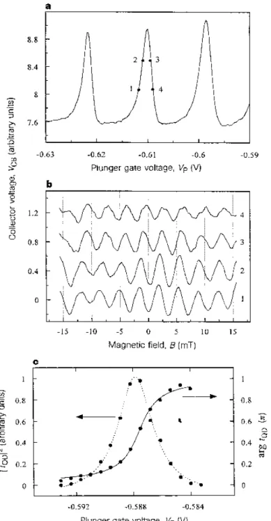
The Aharonov–Bohm phase in a two–terminal device is restricted to 0 or π. This phase rigidity which is a general property of closed interferometers does not exist in a double-slit-like interference set-up as realized by a many-terminal device. Schuster et al. [22] used such a device, Fig.1.12, to measure directly the magnitude and the phase of the transmission amplitude through a quantum dot in the Coulomb Blockade regime. The electron micrograph of the device and a schematic description of the experiment are shown in Figs. 1.12, 1.13. The central element of the device is an Aharonov–Bohm ring with a quantum dot embedded in its right arm. Several contacts are connected to the ring, namely the emitter (E), the collector (C) and a base region (B). The base contacts were held at zero chemical potential in order to collect all back-scattered electrons and to ensure that only two forward propagating electron waves reach the collector. The special type of gates, reflectors, were also introduced into the structure of the interferometer. They reflect diverging electrons into the two–slit device and towards the collector. The reflectors were necessary to enhance the collector signal that could otherwise not be measured. All contacts were designed by negatively biased gates on top of the heterostructure.
The quantum dot contained roughly 200 electrons with a mean single–particle level spacing around 55 µeV . The temperature of the two–dimensional electron gas was Tel ≈ 80 mK. The intrinsic (zero–temperature) width Γ of the Coulomb peaks was
estimated to be of the order or even larger than kT . Collector and emitter support only one transverse mode. The quantum dot in this experiment was in the Coulomb Blockade regime.
At low temperatures both the phase coherent length and the elastic mean free path exceed the size of the sample. Then collector current was measured. They observed oscillations of the current as a function of magnetic field with period Φ0. The absence
of higher harmonics (with periods Φ0/n) strongly suggests that the two direct paths
predominantly contribute to the interference.
It the experiment the measured quantity was the voltage drop VCB between
collec-tor and base for a fixed excitation voltage VEB applied between the emitter and the
base. The Aharonov–Bohm interference in the transmission coefficient TEC leads to
an oscillatory contribution to VCB from which the Aharonov–Bohm phase is extracted.
Fig. 1.14(a) shows VCB measured as a function of the gate voltage VP for a fixed
1.2 Measuring the electron transmission phase 29
Figure 1.12: A top-view scanning electron micrograph of the double–slit device used in the Schuster–experiment [22]. The grey areas are metallic gates on the top of the heterostructure. The quantum dot is inserted in the right slit [22].
C E V B B Φ V CB VEB VP
Figure 1.13: Schematic description of the device structure of the double-slit-like exper-iment. An Aharonov–Bohm ring is coupled to an emitter (E), a collector (C) and a base region (B). Reflector gates reflect diverging electrons towards the collector. The quantum dot is designed by the central electrode and the three electrodes on the right hand side of the structure [22].
30 Chapter 1. General introduction
the Coulomb Blockade regime. When the magnetic field is changed, the collector signal shows AB oscillations with the expected period ∆B = Φ0/A where A is the area of the
AB ring. The observed oscillation patterns measured at the four points 1, 2, 3, and 4 close to a resonance are shown in Fig. 1.14(b). The oscillation pattern shifts smoothly as one moves through the resonance. Fig. 1.14(c) displays the phase and the squared magnitude of the AB signal at a resonance peak. The data points are represented by full circles. The phase shows the expected monotonic rise by π over the width of the resonance.
Schuster et al. compared their data with a theoretical model for resonant scattering. They described the coherent part tQDof the transmission amplitude through the dot by
the Breit–Wigner formula [34]
tQD= iCN
ΓN/2
EF − EN + iΓN/2
, (1.10)
where CN is a complex amplitude, EF the energy of the electrons transmitted through
the device, and EN and ΓN the energy and the width of the resonance in the quantum
dot. Both the squared magnitude |tQD|2 and the phase arg tQDare compared with
exper-imental data in Fig. 1.14(c) and are found to be in very good agreement with Eq.1.10. These results clearly show that the transmission through the dot in the Coulomb Block-ade regime is correctly described by a Breit-Wigner formula.
The collector voltage VCB, the magnitude, and the phase of the AB oscillations
measured over a sequence of five peaks are shown in Fig. 1.15. The striking observation is that the phase is very similar at all peaks. The phase increases roughly by π at each peak. Note that the peaks widen and start to overlap as the plunger voltage increases. At the same time, the overall variation of the phase is reduced. The likely origin of these effects is the electrostatic influence of the plunger on the point contacts at the quantum dot. They open slightly with increasing plunger voltage. A striking feature of the data is the sharp phase lapse by π between the resonances. The phase lapse occurs when the magnitude of the AB oscillations vanishes. Using the simple arguments brought by the scattering off a series of distant quasi-localized states the phase of the transmission amplitude should increase by π each time a localized state crosses the Fermi level in the leads. Thus the phase should exhibit a staircase-like behavior and the phase in the neighboring valleys (or peaks) should differ by π. The experimental observations are in contradiction with this result. Numerous works have been devoted to this subject but it seems that a more fundamental explanation is still lacking.
1.2.4.b Experiment of Heiblum. Kondo correlation and unitary limit regimes. Similar experiments were performed using smaller quantum dots [36, 35] compared to the previous ones [21, 22]. In the left arm of the AB interferometer a tiny quantum dot (180 nm × 200 nm) is embedded, Fig.1.16. This quantum dot has a charging energy UC ∼ 1.5 meV and a relatively large single-particle mean level spacing ∆ ∼ 0.5 meV,
allowing strong coupling to the leads without overlapping of the energy levels in the quantum dot. The Kondo temperature for such a quantum dot can be as high as 1.5
1.2 Measuring the electron transmission phase 31
Figure 1.14: Conductance and phase evolution along a Coulomb peak. (a) Resonance peaks as a function of the plunger gate voltage. (b) A series of interference patterns taken at the points specified in (a). (c) Squared magnitude and phase of the Aharonov– Bohm oscillations (dots). The solid and dashed line are fits for the phase and the squared magnitude obtained with a Breit–Wigner model [22].
32 Chapter 1. General introduction -0.60 -0.59 -0.58 -0.57 -0.56 -0.55 0.0 1.0 0.8 0.6 0.4 0.2 15 10 5 0 9 8
a
b
c
Collector Voltage (a.u.)
Magnitude of AB Oscillations (a.u.)
Phase of AB Oscillations
[ ]
Plunger Gate Voltage, V [V] p
π
Figure 1.15: (a) A series of Coulomb peaks; (b) Magnitude of the Aharonov–Bohm oscillations; (c) Phase of the Aharonov–Bohm oscillations as a function of plunger gate voltage. The solid lines are guides to the eye [22].
1.2 Measuring the electron transmission phase 33
Figure 1.16: A top-view scanning electron micrograph of the double–slit device used in the Yang–experiment [35]. The black zones represent 2DEG and the grey areas are metallic gates on the top of the heterostructure. The quantum dot is inserted in the left slit. The barrier gate is added in order to shut off the reference arm and test the bare quantum dot [35].
K. Thus the low-temperature behavior, T ≪ TK, is made accessible for experimental
investigations. The Aharonov-Bohm ring is supplied with a new gate - the barrier gate, which allows to shut off the reference (right) arm and test the bare quantum dot.
First, measuring the conductance through the bare quantum dot (with the pinched off reference arm) Kondo correlations were identified. A peak conductance of ∼ 1.9e2/h
was measured, suggesting that the quantum dot is in the unitary limit regime. The conductance in two neighboring valleys with (presumably) zero net spin in the quantum dot is found to be suppressed as temperature lowered, as it is expected for the Coulomb blockade regime. As the temperature or the dc bias voltage across the quantum dot is increased, a valley is formed and the single broad peak dissolves into two CB peaks, however the conductance of the outer CB valleys increases. This is the typical behavior of a conductance of the quantum dot with Kondo correlations.
The phase and magnitude of the complex transmission amplitude through the quan-tum dot are obtained as previously - from the measurements of the drain current as a function of the magnetic field and plunger gate voltage.
The main results are reported in Fig.1.17. The complex transmission amplitude (phase and magnitude) are plotted vs plunger gate voltage for different couplings be-tween the leads and the quantum dot. Reducing the coupling strength is equivalent to reducing the Kondo temperature TK. The coupling strength gets weaker from (a) to
(d) in Fig.1.17 and the quantum dot moves from the Kondo regime to the Coulomb blockade regime. In the unitary limit the phase exhibits an almost linear growth of 1.5π (a). In the regime (b) it develops a plateau and later, as the coupling weakens further, the quantum dot enters into the Coulomb blockade regime observed in previous experi-ments [22]. In the case of low coupling to the leads and higher temperature, Tel ∼ 100
34 Chapter 1. General introduction
Figure 1.17: The complex transmission amplitude (phase and amplitude) of the quantum dot as a function of energy (plunger gate voltage) for different coupling strengths of the quantum dot to the leads. The coupling gets weaker from (a), the unitary limit, to (d), Coulomb blockade regime [35].
The phase exhibits a striking behavior in the CB valley. While the phase lapse for the quantum dots in the Coulomb blockade regime is always of order of π, the phase in each CB valley returns to zero, the phase lapse in the CB valley following the Kondo valley does not returns to its initial value.
The evolution of the phase and magnitude of the transmission amplitude with in-creasing temperature or bias voltage is also measured. In both cases the Kondo corre-lations are found to be suppressed.
To summarize, two main (troubling) features stand out. The first one is the behavior of the phase as a function of the gate voltage and its large span, twice larger than the theoretically predicted value [37, 38] when the system is in the Kondo regime. The second striking feature is the phase behavior in the CB regime adjacent to the Kondo correlated regime with the existence of the phase lapse or abrupt phase evolutions. The origin of the phase lapses has not been well understood so far.
1.2.5
Theoretical works
In this section we will briefly review the main results obtained for the transmission phase shift.
1.2.5.a Phase shift
One of the first theoretical predictions for the phase shift was made by D. Langreth in 1966. He analyzed the scattering states and calculated the S-matrix in the framework of
1.2 Measuring the electron transmission phase 35
the 3D Anderson model. He showed that the Friedel sum rule is an exact consequence of the Anderson Hamiltonian for the case where there is no local moment. His main conclusion can be outlined in the following way: at zero temperature the sum of all the phase shifts at the Fermi level is equal to π times the charge displaced by the impurity. For the single-level Anderson model in the absence of magnetic field the phase shifts per each spin are equal and each of them takes the value of πn0/2, where n0 is total
occupation of the impurity site.
In the context of quantum dots the important contribution was made by D. Gerland and collaborators in 2000. They analyze the dependence of the transmission phase shift as the function of the energy of the localized level (or applied gate voltage) for a quantum dot in presence of Kondo correlations. The authors assume that the phase shift measured in the Aharonov-Bohm interferometry experiment at zero temperature and magnetic field, coincide with the phase of the retarded Green function of the localized electrons evaluated at the Fermi level. The phase is then calculated using the numerical renormalization group approach (NRG) and Bethe anzats. In this work authors predict that the transmission phase shift of a quantum dot in the presence of Kondo correlations is equal to π/2 in the unitary limit regime. The dependence of the phase shift with bias voltage and temperature is also analyzed and we will come back to this question in Chapter 4.
1.2.5.b Phase lapses
Simple arguments show that the phase in the neighbouring conductance valleys should differ by pi, exhibiting the so called ”off-phase” behaviour that clearly contradicts the experimental observation. The phase slips in each conductance valley by an amount of π, resulting in the so called ”in-phase” behaviour. This phenomenon is largely discussed in the literature. The analysis, however, is restricted only to the case of a quantum dot in the Coulomb blockade regime.
The origin of the phase lapses was first studied by Levy Yeyati and Buttiker [39]. They discussed the subject in terms of the Friedel sum rule. The authors emphasized that one has to take into account the additional charge induced in a conduction region which includes not only the quantum dot but also the Aharonov-Bohm ring. In a model calculation for a two terminal device using proper values of the extra charge, sequences of two or three consecutive in-phase resonances are found.
The connection between the Friedel sum rule and the phase lapses was reconsidered by Lee [40] and Taniguchi and Buttiker [41]. They conclude that the transmission phase shift can deviate from the Friedel sum rule at some special points where the transmission through the quantum dot vanishes. A transmission zero corresponds to a singular point of the transmission phase. The phase jumps abruptly by pi when the system is swept through the transmission zero. The authors also show that the spatial dimension of the scattering region is important: while the neighbouring resonances are always off-phase in strictly 1D systems, both off-phase and in-phase resonances can be found in higher dimensional systems.
36 Chapter 1. General introduction
Weidenmuller [42] for the weak coupling regime Γ < T < ∆ where Γ is the width of the resonance, T is the temperature and ∆ is the mean level spacing. In this regime the transmission amplitude can be reduced to a sum of Breit-Wigner resonances. The obtained phase shows an increase by π on the scale T at each resonance. Between each resonance, the phase slips by π on the scale of the resonance width Γ.
In 1998, a number of authors [43, 44, 45, 46] studied models for the transmission through a quantum dot and found abrupt jumps of the transmission phase. The jumps occurred at singular points where the magnitude of the transmission amplitude vanishes. Transmission zeros were found in numerical studies exploring Fano resonances [43, 44, 45] and the interplay with multiple resonances [46]. In Refs. [43, 44, 45] a quantum dot is modelled as a quasi-1D or 2D region. A more general approach to the connection between transmission zeros and in-phase resonances was presented by Lee [40]. He showed that the transmission always vanishes between neighbouring in-phase resonances, provided that the scattering region is connected to two single-channel leads and the system is time-reversal invariant.
In spite of all these efforts a more fundamental explanation is lacking. Each of the proposed mechanisms can be criticized since they rely on some given assumption.
Chapter 2
Theoretical analysis of the
transmission phase shift of a
quantum dot at zero temperature in
the presence of Kondo correlations
38
Chapter 2. Theoretical analysis of the transmission phase shift of a quantum dot at zero temperature in the presence of Kondo correlations
2.1 Introduction 39
2.1
Introduction
We study the effects of Kondo correlations on the transmission phase shift of a quan-tum dot coupled to two leads in comparison with the experimental measurements made by Aharonov-Bohm (AB) quantum interferometry. We propose here a theoretical in-terpretation of these results based on scattering theory combined with Bethe ansatz calculations. We show that there is a factor of 2 difference between the phase of the S-matrix responsible for the shift in the AB oscillations, and the one controlling the conductance. Quantitative agreement is obtained with experimental results for two different values of the coupling to the leads.
Quantum dots (QD), small puddles of electrons connected to leads, can be obtained in a controlled fashion thanks to recent progress in nanolithography. Under certain conditions a dot can be modeled as a localized spin coupled to Fermi baths (the leads). A Kondo effect takes place [29, 47, 32] when the temperature is lowered . A key ingredient of the Kondo effect is the phase shift δ an electron undergoes when it crosses the dot. While its direct measurement was out of scope in bulk systems, it became feasible recently in quantum dots via Aharonov-Bohm (AB) interferometery [36]. We mention here the experimental results obtained in two cases corresponding to a strong coupling to the leads [36, 35]. In the unitary limit, the phase shift climbs almost linearly with VG
with a value at the middle of the Kondo enhanced valley which is almost π. At a smaller value of the coupling strength, the phase shift develops a wide plateau at almost π. We will call the latter case the ”Kondo correlation regime”. Early theoretical work on the phase shift for the bulk Kondo effect [37, 48] predicts δ = π/2. In the context of QD, Gerland et al [38] had obtained, on the basis of NRG and Bethe ansatz calculations, a variation of δ with the energy of the localized state leading to a value of π/2 in the symmetric limit, in disagreement with the recent experimental results quoted above [36, 35]. In this chapter, we propose a new theoretical interpretation of the experimental results based on scattering theory and Bethe ansatz calculations. Our main prediction concerns a factor of 2 difference found between the phase of the S-matrix observed by the phase shift measurements and the phase governing the conductance.
2.2
Scattering Phase Shift
2.2.1
Two-reservoir Anderson model
Let us consider a quantum dot coupled via tunnel barriers to two leads L and R, and capacitively to a gate maintained at the voltage VG. Following Glazman and Raikh
[49] and Ng and Lee [50], one can describe the system by a generalized one-dimensional Anderson model in which the localized state of energy ε0 lies at the i = 0 site, and
the sites i ≤ −1 (i ≥ 1) simulate the left and right reservoirs. The corresponding hamiltonian is written as follows
40
Chapter 2. Theoretical analysis of the transmission phase shift of a quantum dot at zero temperature in the presence of Kondo correlations
Figure 2.1: A schematic representation of the one-dimentional Anderson model (left). The i = 0 site represents the localized state of energy ε0. The model can be sketched in
another way (right) which indicates the inner structure of the impurity.
H = −V X σ X i≥1 (c†i,σci+1,σ+ h.c.) −V X σ X i≤−2 (c†i,σci+1,σ + h.c.) − VR X σ (c†0,σc1,σ + h.c.) − VL X σ (c†−1,σc0,σ+ h.c.) (2.1) +ε0 X σ n0σ+ U n0↑n0↓,
where the operator c†i,σ creates a conduction electron on site i with spin σ = ±1/2 and c†0,σ creates an electron on the localized state at the site 0 while n0σ = c†0,σc0,σ is the
occupation number of the localized state with spin σ. U is the Coulomb interaction between two electrons of different spins on the localized state and V , VRand VL are the
hopping integrals between neighboring sites. The parameters VR and VL simulate the
potential barriers between the impurity site and the left and right reservoirs respectively. In realistic systems, the i = 0 site represents a localized state of energy ε0; the parameters
VRand VL generally are small as they decrease exponentially with the distance between
the localized site and the left or right electrode. This model is very similar to the one-impurity Anderson model with the impurity d orbital replaced by a localized state and the conduction band replaced by left and right Fermi seas. The distinct feature of the model described by the Hamiltonian Eq.2.1 from the one-impurity Anderson model is that the left and right Fermi seas in general may have different chemical potentials so that the out of equilibrium properties of the system can be investigated. Here we will focus on the equilibrium situation. In this case both models are equivalent. We will come back to this question later when we will discuss the value of the occupation number, n0.
![Figure 1.2: Temperature dependence of the resistivity for different concentrations of impurity atoms - comparison between experiment (circles) and theory (curves) [4].](https://thumb-eu.123doks.com/thumbv2/123doknet/12881349.370046/14.892.283.594.243.643/temperature-dependence-resistivity-different-concentrations-impurity-comparison-experiment.webp)
![Figure 1.6: Conductance as a function of V G for different temperatures. T ranges from 15 mK (black trace) up to 800 mK (red trace) [32].](https://thumb-eu.123doks.com/thumbv2/123doknet/12881349.370046/23.892.168.693.200.557/figure-conductance-function-different-temperatures-ranges-black-trace.webp)
![Figure 1.8: Electron micrograph of the Aharonov-Bohm interferometer used in the [21].](https://thumb-eu.123doks.com/thumbv2/123doknet/12881349.370046/25.892.249.621.199.487/figure-electron-micrograph-aharonov-bohm-interferometer-used.webp)
![Figure 1.12: A top-view scanning electron micrograph of the double–slit device used in the Schuster–experiment [22]](https://thumb-eu.123doks.com/thumbv2/123doknet/12881349.370046/30.892.279.620.195.499/figure-scanning-electron-micrograph-double-device-schuster-experiment.webp)

![Figure 2.7: Experimental conductance G exp (V G ) (red squares) and phase shift Φ(V G ) (blue triangles) as a function of the gate voltage V G (values taken from Ref.[35] incor-porating a shift in the V G -scale for G exp (V G ) evaluated to ∆V G = 15mV ,](https://thumb-eu.123doks.com/thumbv2/123doknet/12881349.370046/52.892.200.705.193.581/figure-experimental-conductance-squares-triangles-function-porating-evaluated.webp)

