HAL Id: hal-02154088
https://hal-centralesupelec.archives-ouvertes.fr/hal-02154088
Submitted on 18 Dec 2020
HAL is a multi-disciplinary open access
archive for the deposit and dissemination of
sci-entific research documents, whether they are
pub-lished or not. The documents may come from
teaching and research institutions in France or
abroad, or from public or private research centers.
L’archive ouverte pluridisciplinaire HAL, est
destinée au dépôt et à la diffusion de documents
scientifiques de niveau recherche, publiés ou non,
émanant des établissements d’enseignement et de
recherche français ou étrangers, des laboratoires
publics ou privés.
Printed copper connections on flexible substrates
Nataliya Kalashnyk, Sophie Noël, Pascal Chrétien, Aurore Brézard-Oudot,
Thierry Leblanc, Frédéric Houzé, Fanny Hauquier, Vincent Derycke, Thomas
Berthelot, Didier Rousseau
To cite this version:
Nataliya Kalashnyk, Sophie Noël, Pascal Chrétien, Aurore Brézard-Oudot, Thierry Leblanc, et al..
Printed copper connections on flexible substrates. 65th IEEE Holm Conference on Electrical Contacts,
Sep 2019, Milwaukee, United States. pp.350-358, �10.1109/HOLM.2019.8923847�. �hal-02154088�
Printed copper connections on flexible substrates
N. Kalashnyk1 S. Noël1 P. Chrétien1 A. Brézard-Oudot1 Th. Leblanc1 F. Houzé1 F. Hauquier2,3 V. Derycke3 T. Berthelot4 D. Rousseau4.
1
GeePs - Group of electrical engineering Paris, UMR CNRS 8507, CentraleSupélec, Univ. Paris-Sud, Université Paris-Saclay, 11 rue Joliot-Curie, Plateau de Moulon, 91192 Gif-sur-Yvette, France
2IRAMIS/NIMBE/LICSEN, 3CEA, Centre d'Etudes de Saclay, 91191 Gif-sur-Yvette Cedex, France. 4
Kelenn Technology, 4 rue Ampère, 91430 Igny, France
Abstract— This paper presents our first results on printed copper
connections on flexible organic substrates obtained in a single-step process. Many progresses have been made in the field of conducting inks and printing systems and potential applications are within reach. Nowadays the most common conducting inks involve silver nanoparticles. However this solution presents some drawbacks like the high cost of these inks due to the base metal and to the synthesis and also their tendency to clog nozzles in industrial inkjet printheads. For these reasons we have started a program on copper inks for the formation of conducting, homogeneous and adherent connections on polyethylene terephthalate films in view of applications in the field of flexible electronics. The main challenge is to print copper patterns on PET with an industrial process that would present a high time to readiness level. Multiple technical obstacles are addressed: i)- The ink needs to be nanoparticle free: we have chosen a metal organic decomposition ink (MOD) where copper salts are combined with ligands and additives, ii) it must be compatible with an inkjet system in terms of viscosity, rheology and iii) the printed copper must be conducting and adherent. This means that reduction of copper ions must be achieved using a post-printing treatment harmless to the substrate. Intense Pulsed Light was chosen. Printed patterns were characterized by various means: macroscopic electrical behaviour by 4 probe measurements, microscopic electrical behaviour by conducting probe Atomic Force Microscopy (AFM). Morphological and chemical analyses were also performed. It is shown that in optimised conditions good conductivity can be achieved. Much work is still needed to fully understand the mechanisms involved and realize electronics circuits.
Keywords-component; copper interconnection, Metal Organic Decomposition ink, jet printing, Intense Pulsed Light treatment.
I. INTRODUCTION
This work aims at understanding and finding the proper conditions to print copper interconnections on low temperature polymer substrates such as PET (polyethylene terephthalate). Many very complete literature reviews have been published lately on conductive inks for printed electronics. In 2014 Wunscher et al. compiled 245 references on sintering of metal inks [1]; in 2015 Abhinav et al. compiled 136 references on
copper conductive inks [2], in 2017 Lim et al. compiled 113 references on intense pulsed light curing [3] and in 2018 Raut et al. compiled 200 ones on inkjet printing metals for flexible electronic [4]. This is a large set of references to refer to. Nevertheless little has been reported on IPL (Intense Pulsed Light) sintering of printed MOD inks on PET. Much of the work reported concerns print screening deposition process, nanoparticle inks, thermal post treatments at relatively high temperature in inert gas for 30 min or so but they are very valuable source of information.
II. SAMPLESANDEXPERIMENTALTECHNIQUES
A. Samples
The substrate is a PET foil 125µm thick from Normandy Coating France. The metallic salt inks chosen are based on formulation of the metal organic decomposition (MOD) ink which have been reported to be reduced to metallic copper [5-8]
Several formulations have been studied based on copper formate (C2H10CuO8) and AMP
(2-amino-2-methyl-1-propanol) complexes (Cuf-AMP) as described in [6, 7].
The paper does not present the multiple formulations tested but summarizes the main steps of a collaborative research project funded by Agence Nationale de la Recherche. The copper formate AMP complexe (denoted Cuf-AMP) inks were purchased from Gene’Ink –Rousset France). Various solvents, additives, binders were used for the preparation of several batches all having in common low surface tension values (27 mN/m<γ<28 mN/m), low viscosities at 20°C (9.6 cP<η< 12.5cP), densities around 1 and pH values in the range 7.4 to 8.4. These characteristics allowed to jet print patterns on PET sheets.
In a first step a Dimatix DMP-2831 printer was used with the following printing parameters: drop volume 10pL, drop spacing 35µm, bed temperature 50°C. Fig.1 a) shows the ink while Fig.1 b) shows an example of drops printed on the PET film. Several passes were needed to obtain better homogeneity of the films.
The films were then sintered with an intense pulsed light lamp (IPL) the Xenon S2200 (fitted with a B lamp 240nm -1100nm). When the sample was exposed to the pulse light a complex process took place resulting in local decomposition of the copper MOD ink without damaging the substrate [8].
Several settings were possible, changing the pulse duration, the cooling off duration, the total energy and the number of pulses [9].
The major difference of this work with the published literature is that its purpose was to propose a process for industrial manufacturing: therefore the inks are MOD type inks to avoid nanoparticules, the printing is direct and fast which has its drawbacks (thin films that can be uneven), the curing process is performed in air and is very fast as is expected for a production line.
Therefore one of the major difficulties was to assess the performances of the IPL sintering settings without interference of the quality of the printing. Thus a very large number of samples were prepared and analyzed.
Figure 1. Cu formate AMP (Cuf-AMP) complex dissolved in solvents; visualisation of printed drops incompletely transformed by IPL sintering.
B. Characterization techniques and experimental test
Several techniques were used to evaluate the inkjet printed patterns.
Electrical characterisation 1)
a) 4 point resistivity measurements :
Electrical measurements were performed with a Signatone Pro4 4 point probe resistivity device; the four point probe head specifications are: 1.587 mm tip spacing, 0.254 mm tip radius and 45 gf normal load on each tungsten carbide tip. The aim was to quickly assess the macroscopic conductivity of the films.
b) Conductive probe Atomic Force Microscopy (AFM) AFM topography and electrical maps were obtained with a Bruker MultiMode8 equipment fitted with a special home-made amplification and conversion device, called Résiscope (referred to as CP-AFM) in order to acquire simultaneously topographic and electrical images of the surfaces using doped diamond coated tips (radius ≈ 150 nm). The intrinsic resistance
of these probes is about 5 kΩ. The aim was to have a local evaluation of the conduction in relation to the topography.
c) V(I) curves and surface temperature measurements V-I measurements were performed with a 2450 Keithley Sourcemeter. During some of the runs the sample was filmed with a Jade MWIR camera (Cedip) calibrated with a black body for copper sample. The rate of acquisition was 1Hz to measure the increase of the surface temperature with the current flow. The spectral response of the InSb detector was in the range 3.5 µm - 5.1 µm. The range of temperature was 5-150°C. The aim was to evaluate the possibility of an application.
Composition 2)
Transmission measurements were achieved by means of a modified Fourier Transform Infrared (FTIR) spectrometer that allows measurements in the range 350-1800 nm within a few seconds with a resolution of the order of a nanometer as described in [10].
The surface chemical composition was analyzed with a PHI 5000 Versaprobe multi-technique XPS using a monochromatic Al Kα source. The system was calibrated with Cu 2p3/2 and Cu LMM of clean copper at 932.7 eV and 918.7 eV respectively. The take-off angle was 45°. Charging was compensated by a very low electron beam.
III. RESULTSANDDISCUSSION
A. Uniform film printing
The Cuf-AMP MOD inks were printed on the PET sheets to form square patterns (10mm x 10mm) for all the experiments.
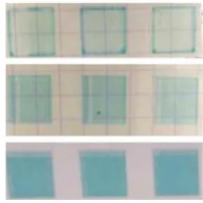
Figure 2. Ink jet -printed patterns of Cu formate MOD ink with increasing number of passes; a) 1 pass, b) 3 passes and c) 5 passes.
Fig.2 shows samples patterns printed with 1 pass, 3 passes and 5 passes. The film thickness is observed to increase with the number of passes. For one pass the film is very transparent and side effects can be observed.
Formation of drops on the surface depends of the surface energy of the substrate, the surface tension of the ink, the atmosphere and the temperature of the substrate holder. Complex mechanisms can occur when there is a mixture of
various solvents: edge effects, dewetting, Marangoni effect. The chosen inks had good wetting properties; some printing defects can nonetheless be observed on some of the samples.
These patterns were almost liquid and the thickness was not easily measurable. Most of the characterizations were thus performed after the photonic treatment.
B. Sintering of the the ink patterns
In order to avoid degrading the PET substrate (softening temperature 70°C and melting point 250°C) IPL treatment was chosen to transform the Cu(II) ions into a metallic film.
The self-reduction of metallic copper salt inks has been reported to occur at temperatures around 200°C (though some work report heating the ink patterns as high as 350°C in reductive and inert atmosphere). The high energy light pulses can be used to control the chemical transformation of copper (II) salt into metallic copper.
The IPL device has a light emission spectrum in the UV-vis-IR range as shown in Fig.3.
Figure 3. Emission spectrum of the Xenon S2200.
When the sample is exposed to the pulse light, complex physical process can induce thermal decomposition of the copper MOD ink. IPL sintering of nanoparticle inks has been described by many authors but far less papers deal with IPL transformation of MOD inks. From Rosen’s work [5] we know that decomposition of MOD ink with photonic curing occurs in two steps. First the copper ions absorb light (600 – 800 nm range) causing the excitation of electrons and local heating, Afterwards the rise in energy is sufficient to enable the decomposition of the copper formate to copper, carbon dioxide and hydrogen along with a reduction of the copper ions to pure copper.
Transformation seems to be dependent to the absorbance properties of the inks. Transmission spectrum of the ink recorded was recorded as in [10] and the absorption deduced as shown in Fig.4.
Figure 4. Absorption spectrum of a Cuf AMP ink printed on PET.
The reduction of the copper salt also depends on the light pulse characteristics. Unfortunately there is no data or practical examples on the optimal IPL parameters for the decomposition of copper MOD ink and the resulting morphology and conductivity. Many tunings had to be chosen for the Xenon S2200.
Fig.5 shows the major parameters: number of pulses, energy per pulse, duration of the light pulse tp, duration of the cooling off td. Too high a value of the power led to ablation and burning of the substrate and not enough power to partial transformation.
Figure 5. IPL waveform showing the pulses: number duration and time off.
Three transient curing conditions have been established by Schroder [11, 12]. Considering a film of thickness xf with thermal equilibration time τf siting on a substrate with thickness es and equilibration time τs these conditions can be written as:
- xf<<es, the thickness of the film must be much smaller than that of the substrate so that the substrate acts as a thermal mass cooling the film.
- tp<<τs, the film heating is completed before the substrate can heat up.
- τf<<tp, τf is affected by the film porosity and remaining solvents. -td tp E ( a. u. ) t (a.u.)
Fig.6 shows a printed pattern before and after the IPL sintering of the copper MOD ink.
Figure 6. Printed Cuf MOD before and after an IPL exposure. The blue color is indicative of Cu(II) ions and the brownish one of transformed films.
The energy sent to the sample was calibrated with a dedicated Nova II P/N 7201550 laser power and energy meter fitted with a L50(150)A probe with a 50mm diameter. For clarity and for the purpose of comparisons with literature, Table I gives the values of the energy as programmed on the Xenon S2200 (in Joule) and the value of the calibrated energy in J/cm2.
A few examples of the settings we used are given here.
TABLE I. IPL SETTINGS
Sample IPL (a) (b) (c) (d)
E* (total) (J) 3600 4100 5100 10300 E (measured) (J/cm2) 24.5 27.9 34.7 70.14 Pulse duration tp (ms) 1.8 1.2 1.5 0.6 Time off duration toff (ms) 300 200 200 100 n pulses 5 10 10 50 Total light exposure (ms) 9 12 15 30 Power density (kW/cm2) 2.72 2.32 2.31 2.33
E* total as set on the Xenon S2200
C. Characterizations of the sintered printed films Sheet resistance
1)
Sheet resistance values (Rs) were measured at several locations on the inkjet printed patterns submitted to various IPL treatments. Burned samples and incompletely transformed samples were discarded. Fig.7 shows a statistical plot of the values obtained.
The first observation is that films with various conductivity properties were obtained. The mean values here range from 24 Ω/□ to 5552 Ω/□ and the standard deviations range from 9.6 Ω/□ to 12 553 Ω/□. Conductive films were successfully obtained, the lowest value of Rs being bellow 10 Ω/□.
Figure 7. Statistical plot of Rs (Ω/□) sheet resistance measurements on printed patterns after various IPL sintering conditions.
The second observation is that changing the energy, the number and duration of the pulses has an effect on the conductivity. For an assessment it is easier to look at Fig.8 where the mean values of Rs are plotted for given energy values and the corresponding power density values.. The minimum mean sheet resistance value is obtained for lowest energy and for the maximum power density of 2.7 kW/cm2. For higher energies and lower power Rs values are higher. Also for the highest energy (70.14 J/cm2) Rs values are very high and scattered.
Figure 8. Values of sheet resistance Rs at given power density and programmed energy conditions.
This is in agreement with authors reporting that curing depends on power density. Note that with the 4 point probe it was impossible to measure many samples, either because they were totally insulating or because proper contacts could not be established for all four probes due to the inhomogeneity of the film topography. 101 102 103 104 105 0 20 40 60 80 100
C
um
ul
a
tiv
e %
Rs (Ω/sq)
(d) (c) (b) (a) 10 100 1000 2.0 2.5 3.0 3.5 4.0 4.5 5.0 5.5 6.0 20 30 40 50 60 70P
ow
er
(
kW
/c
m
2)
Rs (Ω/sq)
(d) (b) (c) (a)E
ner
g
y (
J
/c
m
2)
Figure 9. Optical images A) sample with IPL (a) and B) sample with IPL (d). The arrow on the left images is 10mm; the right images are higher
magnifications.
Fig.9 shows optical images of the 10 mmx 10mm samples with IPL curing conditions (a) and (d). Higher magnification images are also shown.
CP AFM 2)
We have then measured the electrical properties of the films at a more local scale with the CP AFM technique. In these experiments the conducting tip was pressed on the film with a low load (150 nN for a probe with a radius of 150 nm) and the connection to the measuring device was established by silver paste at a distance of about 5 mm. Note that the substrate is PET and totally insulating so that conduction occurs in the plane of the ink layer. Topographic and electrical images are shown here for the best (IPL (a)) and the worse (IPL (d)) above treatments.
Fig. 10 shows the typical aspect of the surface when scanning on different locations of the sample treated with condition (a). The pink regions on the electrical image correspond to tip/surface resistances higher than 1012 Ω. This is due to a carbon contamination film thicker than a nanometer. (see XPS analyses below). Surprisingly despite this carbon film conductive islands are measured (from a few 103 to 105 Ω) which indicate that a connecting path exists to the collecting electrode 5 mm away.
Figure 10. CP AFM images of copper MOD ink with IPL treatment (a)
The profiles of Fig.11, extracted from the images of Fig.10 show a correlation between emerging particles and conduction. This is a major indication that copper particles were formed during the IPL treatment and build a 3D network.
Figure 11. Height profil a) and electrical profile b) extracted from Fig.10.
The scans of sample IPL (d) were very different. Two different locations of the sample are shown in Fig. 12 and 14 with typical profiles in Fig. 13 and 15.
Figure 12. CP AFM images of copper MOD ink with IPL treatment (d) location 1.
Figure 13. Height profil a) and electrical profil b) extracted from Fig.12.
a)
b)
x:µm z: nm
x:µm z: log(R)
x:µm z: nm
x:µm z: log(R)
a)
b)
A)
B)
The topography of the second location is much more disturbed with peak to peak height over 1.5 µm. Also the surface exhibits spots with more various values of conductivity. Some spots have the lowest resistance measurable (in the range 103 to 104 Ω which is the tip resistance value) and some show intermediate values (≈107 Ω).
Figure 14. CP AFM images of copper MOD ink with IPL treatment (d), location 2.
Figure 15. Height profile a) and electrical profile b) extracted from Fig.14.
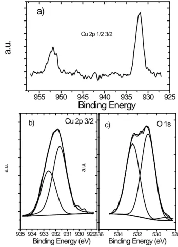
Composition analyses 3)
XPS analyses were performed on some of the IPL sintered samples in order to investigate the film uppermost composition. The main element on the surface is carbon (see TABLE II).
TABLE II. COMPOSITION OF THE PRINTED FILM OF FIG.10.
%at C O Cu N
81.3 17.7 0.6 0.4
It comes from the atmosphere contamination but also from by-products formed during the exposure to the flash light and a possible incomplete decomposition of the copper formate AMP complex. This is visible on the magnified optical images of Fig.9. A copper signal was nonetheless measured and the 2p 3/2 and 1/2 peaks are shown in Fig.16 a). The well-known shake-up satellite found indicating Cu(II) species is absent, attesting of the reduction of the copper formate ions. This is in
good agreement with the macroscopic conductivity of the films (low sheet resistance) and the highly conducting spots seen on the electrical AFM images.
A proposed decomposition for the Cu 2p 3/2 peak is shown in Fig.16 b). After correction for the charge (positioning the main C1s peak at 284.6 eV) the peaks binding energies are at 932.7 eV and 933.7 eV. These can be assigned to metallic copper or Cu2O for the first one and to Cu(OH)2 for the second
one. The corrected Auger parameter [13] which can be expressed as α’=Ek(AES)+EB(ph), is the sum of the binding energy of a pic and the kinetic energy of the corresponding transition; it usually helps to determine the oxidation state of copper Cu. Here the Cu Auger L3M45M45 (not shown here) seems to be
display extra structures [14] deserving further investigations. The oxygen 1s peak Fig.16c) has a component at 531.9 eV corresponding to O=C and a component at 533.5 eV and the carbon C1s peak (not shown here) indicates the presence of O-C=O. These two peaks do not correspond to the Cuf-AMP spectra and could correspond either to underlying PET and/or by-products formed during the IPL sintering exposure.
Figure 16. XPS spectra of IPL treated copper MOD printed pattern.. a) Cu 2p 3/2 and Cu 2p ½, b) Cu 2p 3/2 with decomposition, c) O1s with
decomposition
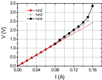
V(I) measurements with increasing current. 4)
V(I) curves were measured on a sample of type (a) having a low sheet resistance values; silver paste side electrodes were
x:µm z: nm
x:µm z: log(R)
a)
b)
935 934 933 932 931 930 929 b) Cu 2p 3/2 a. u.Binding Energy (eV)
536 534 532 530 528
c) O 1s
a.
u.
Binding Energy (eV)
955 950 945 940 935 930 925
a)
Cu 2p 1/2 3/2a.
u.
Binding Energy
used for the measurement. When increasing the current above a certain value, the increase of resistance gave a voltage value higher than the compliance of the Keithley; the sample was destroyed. Further runs on other equivalent samples were then performed with the simultaneous recording of the surface temperature with a thermal camera. A first run at low current attested of the good connection. During the second run the current was increased in steps of 10 mA (for 4 min) up to 100 mA with simultaneous measurements of I, V and the surface temperature. Fig.17 shows good linearity, with R varying from 15.2 Ω to 15.8 Ω while. Fig.18 plots the temperature integrated over a large central area of the sample. It shows that the surface temperature increases with the current but stabilizes during the current steps. The thermal images presented in Fig.19 show that the surface temperature is rather constant over the whole pattern indicating a rather homogeneous film despite the presence of a possible by-product matrix.
During the third run with the same sample, varying I from 80 mA to 150 mA, an increase in the resistance value was recorded at 140 mA. In the fourth run the current intensity was increased higher up to a value of 160 mA. The temperature evolution can be observed to stabilize during the current steps up to the same value of 140 mA (Fig. 20).
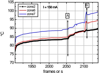
Fig.21 shows the temperature evolution during the 150 mA plateau. After applying the current for 2 min the temperature rises a first time and then a second time a few seconds later. Because of the local changes occurring, the temperature was integrated on the large central zone (labelled 2) but also on two smaller ones referred to as zones 6 and 7, the positions of which are indicated on the thermal images. These images Fig.23 A) and B) show the inhomogeneity of temperature on the printed pattern. Some zones do not radiate any longer and some become very intense. The temperature rise since the beginning of the current step can be evaluated locally at 20°C on zone7.
Fig.22 shows the 160 mA plateau; after a few seconds (14 s) the compliance of the Keithley being reached, the sample does not conduct anymore. The thermal images of Fig.23 C) and D) show very bright spots (with an estimated surface temperature of 120°C) and the rapid cooling down.
Figure 17. Voltage current curves for IPL sintered Cuf MOD pattern.
Figure 18. Evolution of the surface temperature (in black) with time at increasing levels of I (in red); run2. Frame A (954 s) and frame B) 2173 s)
Figure 19. Thermal images showing the temperature evolution during V(I) measurments of run 2. Fig.12 A) frame I= 40 mA and B) frame I=90 mA.
0.00 0.04 0.08 0.12 0.16 0.0 0.5 1.0 1.5 2.0 2.5 3.0 3.5 run2 run3 run4
V (
V)
I (A)
0 200 400 600 800 1000 1200 1400 1600 1800 2000 2200 2400 25 30 35 40 45 0 10 20 30 40 50 60 70 80 90 100 (° C) Frame or s B A I ( mA )Figure 20. Evolution of the surface temperature (in black) with time at increasing levels of current (in red); run4.
Figure 21. Evolution of the surface temperature during the during step I=150 mA integrated on area 2, 6 and 7 as shown on the thermal images of
Fig.23; A (after 2055 s) and in B (after 2108 s).
Figure 22. Evolution of the surface temperature during the step at 160 mA integrated on the same areas as in Fig. 21.
Figure 23. Thermal images showing the temperature evolution during V(I) measurments of run 4, Fig.21. A) frame at 2055 s and B) frame at 2108 s. both for 150 mA. C) frame at 2150 s and D) frame at 2155 s just before
breakdown both at I=160 mA.
IV. CONCLUSION
This work has shown that it is possible to directly print by inkjet process copper MOD ink patterns that can be sintered by intense pulse light to produce conductive patterns. This sintering process performs in air contrary to many of the reported work. At this point the conductivity levels (sheet resistance around 10Ω/□) can allow the process to be involved in low level devices or circuits. The demonstration that copper formate ions are reduced in metallic copper indicates that more work on the IPL sintering conditions could increase the conductivity. In a further step the patterns are now printed on an industrial printer able to work in sheet to sheet mode or roll to roll (Kelenn KSCAN-PE).
ACKNOWLEDGMENT
This work was partly financed by ANR project Photonin’. The authors wish to thank C. Longeaud for the transmission measurements and D. Alamarguy for the XPS measurements with the Versaprobe surface analysis system acquired with fundings by: Region Ile-de-France, Agence Nationale de la Recherche, Centre National de la Recherche Scientifique.
REFERENCES
[1] S. Wünscher et al. “ Progress of alternative sintering approaches of inkjet-printed metal inks and their application for manufacuting of flexible electronic devices”, Journal of Materials Chem. C, 2, 2014, pp. 10232-10261.
[2] V. Abhinav et al. “ Copper conductive inks: synthesis and utilization in flexible electronics”, RCS Advances, 5, 2015, pp. 63985-64030. [3] H. S. Lim et al. “ Intense pulsed light for split-second structural
development of nanomaterials”, Journal of Materials Chem. C, 5, 2017, pp.27142-7160. 0 200 400 600 800 1000120014001600180020002200 30 40 50 60 70 80 90 100 0 20 40 60 80 100 120 140 160 180 200 T (° C) Frame or s I ( mA ) I (mA) 1950 2000 2050 2100 70 75 80 85 90 95 100 105 zone2 zone6 zone7 frames or s I = 150 mA B A °C 2160 2200 2240 2280 2320 2360 70 80 90 100 110 120 I = 160 mA D C zone2 zone6 zone7 °C frame or s
[4] N. C. Raut et al. “ Inkjet printing metals on flexible materials for plastic and paper electronics”, Journal of Materials Chem. C, 6, 2018, pp. 1618-1641.
[5] Y. S. Rosen et al. “ Self-reducing copper precursor inks and photonic additive yield conductive patterns under intense pulsed light”, ACS Omega, 2, 2017, pp. 573-581.
[6] Y. Farraj et al. “ Self-reduction of a copper complex MOD ink for inkjet printeing conductive patterns on plastics”, ChemComm, 51, 2015, pp. 1587-1590.
[7] D-H. Shin et al. “ A self-reducible and alcohol-soluble copper-based metal-organic decomposition ink for printed electronics”, Applied Materials and Interfaces, 6, 2014, pp. 3312-3319.
[8] B-Y. Wang et al. “ Cu ion ink for flexible substrate and highly conductive patterning by intense pulsed light sintering”, Applied Materials and Interfaces, 5, 2013, pp. 4113-4119.
[9] S. J. Joo, “ Highly conductive copper nano/microparticles ink via flas light sintering for printed electronics”, Nanotechnology, 25, 2014, pp.265601.
[10] N. Puspitosar et al. “ Modification of an FTIR spectrometer for optoelectronic characterizations”, Rev. Sci. Instrum., 88, 2017, pp. 086112.
[11] K. A. Schroder “ Broadcast photonic curing of metallic nanoparticle films”, NSTI-Nanotech , 3, 2006, pp.198-201.
[12] K. A. Schroder “ Mechanisms of photonic curing: processing high temperature films on low temperature substrates”, NSTI-Nanotech , 2, 2011, pp.220-223.
[13] C. D. Wagner “The Auger parameter, its utility and advantages: a review”, Journ. Electron Spectros. and Rel. Phenom., 47,1988, pp. 283-313.
[14] E. Antonides et al. “LMM Auger spectra of Cu, Zn,and Ge. II, Relationship with the L23 photoelectron spectra via the L2L3M45