S1
SUPPORTING INFORMATION
The Role of Excitons and Free Charges in the
Excited-State Dynamics of Solution-Processed
Few-Layer MoS
2
Nanoflakes
Demetra Tsokkou1*, Xiaoyun Yu2, Kevin Sivula2 and Natalie Banerji1*
1) Department of Chemistry, University of Fribourg, Chemin du Musée 9, CH-1700 Fribourg,
Switzerland.
2) Laboratory for Molecular Engineering of Optoelectronic Nanomaterials, Institute of
Chemical Sciences and Engineering, École Polytechnique Fédérale de Lausanne (EPFL), Station 6, 1015 Lausanne, Switzerland
Corresponding Authors
S2 1. Estimation of the nanoflake thickness
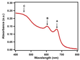
To obtain an estimate of the average number of layers in the solution-processed few-layer MoS2 nanoflake thin films, the absorbance spectrum shown in Figure S1 was used.
FIGURE S1. Absorption spectrum of the few-layer MoS2 nanoflake thin film prepared by the
self-assembly method. The arrows indicate the A, B and C excitonic transition peaks measured at 673, 611 and 453 nm, respectively.
The absorbance peaks at 611 nm (= 2.03 eV) and 673 nm (= 1.84 eV) are associated with the A and B excitonic transitions. These transitions take place at the K point of the Brillouin zone between a local conduction band minimum and two maxima of the valence bands that are largely energetically separated due to spin-orbit coupling.1-2 An additional absorbance peak at higher energies, named excitons C (= 453 nm), is attributed to transitions from the valence band to the nested region of the conduction band or a transition from a deep valence band to the conduction band.3-4 To estimate the average thickness of the MoS2
S3 used and the thickness was found to be ~ 10 nm (representing an average thickness). The deposition method used to prepare the thin film of MoS2 ensures that only one layer of
nanoflakes is deposited on the substrate.6-7 Thus, the average film thickness is used to estimate the average number of atomic layers in these nanoflakes, using the interlayer
stacking distance of the bulk material (~ 0.62 nm) and found to be ~ 16. Taking into account the distribution of different flake thicknesses we estimate that the nanoflakes range from 10-20 atomic layers.
2. Additional TA data
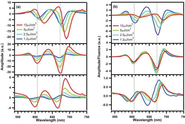
FIGURE S2. (a-c) TA spectra following excitation with a higher photon energy of ~3 eV (410 nm) at a) various time delays and a pump fluence of ~12 μJ/cm2, and at pump fluences between 1.2-12 μJ/cm2 at (b) early (t = 0.2ps) and (c) long (t = 1 ns) times.
S4 TA measurements were also performed using excitation at 400 nm; thus the photoexcited carriers possess more initial excess kinetic energy. The TA spectra at different time delays for an absorbed pump fluence of ~12 μJ/cm2 are shown in figure S2a. Additionally, the TA spectra at early (t = 0.2ps) and long (t = 1 ns) times at pump fluences between 1.2-12 μJ/cm2 are included in Figures S2b and S2c, respectively.
For better visualization of the initial blue-shift observed at short time delays (see discussion in the main text), the TA spectra at fast time delays between 0.1-3 ps for a pump fluence of ~1.1 μJ/cm2 (600 nm excitation) are shown in Figure S3.
FIGURE S3. TA spectra in few-layer MoS2 nanoflakes recorded following photoexcitation at
600 nm at an absorbed pump fluence of ~1.1 μJ/cm2.
Figure S4 shows the results from the global analysis for the TA spectra recorded using excitation at 410 nm at various pump fluences. Similar observations to the ones made for excitation at 600 nm can be extracted. While the fast and show components show a gradual red shift with pump fluence and sub-linear dependence, the intermediate component does not
S5 exhibit any shift even for the highest pump fluence used. Excitation at 410 nm results in the photogeneration of a higher density of charges, thus the shifts observed are larger and the contribution of the charges to the fast relaxation component is more important.
FIGURE S4. a) Amplitude spectra for excitation at 410 nm and different pump fluences between 1.2-12 μJ/cm2 for the fast time constant of 0.5 ps (top), an intermediate one of 5.5 ps (middle) and the long (bottom) component. b) The respective amplitude spectra scaled with the pump fluence are shown.
S6 References
(1) Evans, B. L.; Young, P. A., Optical Absorption and Dispersion in Molybdenum
Disulphide. Proceedings of the Royal Society of London A: Mathematical, Physical and
Engineering Sciences 1965, 284, 402-422.
(2) Frindt, R. F.; Yoffe, A. D., Physical Properties of Layer Structures: Optical Properties and Photoconductivity of Thin Crystals of Molybdenum Disulphide. Proceedings of the Royal
Society of London A: Mathematical, Physical and Engineering Sciences 1963, 273,
69-83.
(3) Kozawa, D.; Kumar, R.; Carvalho, A.; Kumar Amara, K.; Zhao, W.; Wang, S.; Toh, M.; Ribeiro, R. M.; Castro Neto, A. H.; Matsuda, K.; Eda, G., Photocarrier Relaxation Pathway in Two-Dimensional Semiconducting Transition Metal Dichalcogenides. Nat.
Commun. 2014, 5, 4543.
(4) Wilcoxon, J. P.; Samara, G. A., Strong Quantum-Size Effects in a Layered Semiconductor: MoS2 Nanoclusters. Phys. Rev. B 1995, 51, 7299-7302.
(5) Beal, A. R.; Hughes, H. P., Kramers-Kronig Analysis of the Reflectivity Spectra of 2H-MoS2 , 2H-MoSe2 and 2H-MoTe2. J. Phys. C: Solid State Physics 1979, 12, 881.
(6) Yu, X.; Prévot, M. S.; Sivula, K., Multiflake Thin Film Electronic Devices of Solution Processed 2D MoS2 Enabled by Sonopolymer Assisted Exfoliation and Surface
Modification. Chem. Mater. 2014, 26, 5892-5899.
(7) Yu, X.; Prevot, M. S.; Guijarro, N.; Sivula, K., Self-Assembled 2D WSe2 Thin Films for