HAL Id: hal-02962708
https://hal.archives-ouvertes.fr/hal-02962708
Submitted on 3 Nov 2020
HAL is a multi-disciplinary open access
archive for the deposit and dissemination of
sci-entific research documents, whether they are
pub-lished or not. The documents may come from
teaching and research institutions in France or
abroad, or from public or private research centers.
L’archive ouverte pluridisciplinaire HAL, est
destinée au dépôt et à la diffusion de documents
scientifiques de niveau recherche, publiés ou non,
émanant des établissements d’enseignement et de
recherche français ou étrangers, des laboratoires
publics ou privés.
Control of GaN Transistors
Plinio Bau, Marc Cousineau, Bernardo Cougo, Frédéric Richardeau, Nicolas
Rouger
To cite this version:
Plinio Bau, Marc Cousineau, Bernardo Cougo, Frédéric Richardeau, Nicolas Rouger. CMOS
Ac-tive Gate Driver for Closed-Loop d v /d t Control of GaN Transistors. IEEE Transactions on
Power Electronics, Institute of Electrical and Electronics Engineers, 2020, 35 (12), pp.13322-13332.
�10.1109/TPEL.2020.2995531�. �hal-02962708�
_______________________________________________________________ This research is partially funded by IRT Saint Exupéry grant EPowerDrive.
Author Version – Paper published in IEEE TPEL - https://doi.org/10.1109/TPEL.2020.2995531
Abstract— This paper shows both theoretical and experimental analyses of a fully integrated CMOS active gate driver (AGD) developed to control the high dv/dt of GaN transistors for both 48 V and 400 V applications. To mitigate negative effects in the high-frequency spectrum emission, an original technique is proposed to reduce the dv/dt with lower switching losses compared to classical solutions. The AGD technique is based on a subnanosecond delay feedback loop, which reduces the gate current only during the dv/dt sequence of the switching transients. Hence, the dv/dt and di/dt can be actively controlled separately, and the trade-off between the dv/dt and EON switching energy is optimized. Since GaN transistors have typical voltage switching times on the order of a few nanoseconds,
introducing a feedback loop from the high voltage drain to the gate terminal is quite challenging. In this article, we successfully demonstrate the active gate driving of GaN transistors for both 48 V and 400 V applications, with initial open-loop voltage switching times of 3 ns, due to a full CMOS integration. Other methods for dv/dt active control are further discussed. The limits of these methods are explained based on both experimental and simulation results. The AGD showed a clear reduction in the peak dv/dt from -175 V/ns to -120 V/ns for the 400 V application.
Index Terms— Active gate driver, dv/dt, EMI, electromagnetic interference, GaN, HEMT Transistors, wide-bandgap semiconductor, closed-loop systems, driver circuits, feedback circuits, switching circuits, power electronics.
I. INTRODUCTION
Wide-bandgap (WBG) power devices can be used in power converters to improve both their efficiency and power density. Power transistors that can handle high currents and high voltages based on GaN or SiC technologies are expected to represent a growing market in the coming years. Double-digit annual growth in sales and implementation of WBG power devices in the next five to ten years is expected [1]. A steady-growing market is also expected for aircraft applications [2], where higher DC bus voltages are being implemented and more electrical energy is being embedded to replace hydraulic and pneumatic systems in full electric solutions. However, for the same ON-state RDS_ON resistance, WBG power devices have smaller CGD parasitic capacitors
compared to silicon IGBTs and MOSFETs, leading to faster switching speeds with higher dv/dt values. The difficulties in driving these new WBG transistors present several drawbacks for system designers and involve design trade-offs. For silicon carbide (SiC) technology, previous work [3]-[14] has presented different gate drivers to drive SiC transistors while adapting the previously developed techniques for silicon IGBTs or power MOSFETs. The main adaptations are for higher switching speeds, shorter delay times and switching times and specificities of SiC MOSFETs (e.g., driving voltages). In the context of lower voltages and higher frequencies, for GaN transistors, other solutions have been previously proposed [15], where the design can be optimized for reliability, EMI issues or performance.
Indeed, a high turn-on dv/dt value can induce currents by capacitive coupling (through the CGD Miller capacitance) between the
two transistors in a power commutation-cell, and crosstalk conduction can occur [3],[4]. This phenomenon is also described in the literature as cross conduction and extra-losses and possible failure in inverter-leg operation or synchronous buck can occur. This
Plinio Bau, Marc Cousineau, Bernardo Cougo, Frédéric Richardeau and Nicolas Rouger
CMOS Active Gate Driver for Closed-Loop
dv/dt Control of GaN Transistors
problem is frequently observed with WBG devices because the threshold gate voltages and maximum gate voltage are lower than those in silicon. In addition, the threshold voltage for a SiC device decreases with temperature, which reduces its immunity, whereas some GaN devices are not affected by this property. Another disadvantage of high dv/dt is the use of volume-consuming EMI voltage common mode dv/dt filters [17]. For aircraft applications, the size and weight of such filters are key parameters for the system design [18]. Another disadvantage of high dv/dt values is a drain-source overvoltage during turn-off, mainly due to high related di/dt and the presence of parasitic inductors involved in the switching-loop. Finally, a fourth disadvantage is the high frequency induced common mode and differential mode current in the switching node [5]. Consequently, the common mode transient immunity (CMTI) of isolation barriers must comply with higher dv/dt values [19].
Among all the possible ways to control the dv/dt of a power transistor, several options emulate a CGD external capacitance. In
[20], a method using discrete transistors was proposed to actively drive silicon IGBT devices. In [21], a similar approach was adapted for GaN transistors, with discrete components. This solution has a lower bandwidth, and additional stray inductance between device’s gate and source electrodes and therefore, cannot handle dv/dt’s in the order of 100’s of V/ns. Moreover, in the topology proposed in [21], a higher delay is required for the biasing of the transistors involved in the feedback loop, limiting the capability to operate at higher dv/dt values. When increasing the dv/dt dynamic, the transient behavior of the feedback-loop becomes a key point to address. Indeed, one must avoid a prohibitive delay time to properly bias the several transistors involved in the feedback loop. With faster dv/dt values, it is also critical to limit the direct capacitor coupling between the drain and gate terminals of the power devices, to prevent detrimental effects through Miller coupling. Compared to [21], it is then desired to increase the feedback loop gain and to further reduce the value of the high voltage capacitor required for the active gate drive technique. Due to a smaller capacitor, its integration can also be possible.This paper proposes a novel method with a faster and simpler topology to control the turn-on transient based on a full monolithic CMOS gate driver offering very large bandwidth analog circuits. An improved solution, where all required devices are integrated into one ASIC, following the trend of integration [22]-[24], is presented, discussed and experimentally demonstrated.
II. ACTIVEGATEDRIVERSFORSILICONANDWIDEBANDGAPPOWERTRANSISTORS
The classical trade-off between dv/dt and the amount of switching energy (EON) is discussed in the following section. Then, the
state-of-the-art for gate drivers with dv/dt control for power electronic applications is discussed. Our proposed method is then presented and compared to other approaches.
A. Proposed technique: turn-on control
The proposed active gate driver (AGD) technique is implemented only during turn-on. Indeed, the turn-off switching speed is mainly controlled by the load current amplitude and not directly by the gate driver when using high speed devices in high efficiency applications [25]. Nevertheless, our technique can be easily applied for the active control of the turn-off, should a hard turn-off be required by the application (the high dv/dt at turn off undergone at high load current can thus be limited by dynamically re-biasing the gate slightly higher than its threshold). The effects of temperature, load current and input voltage transients for the proposed technique are not discussed in this article. Without any active gate driving, a simplified expression for dv/dt during turn-on is introduced in (1). The derivative of the drain to source voltage (dvDS/dt) depends on the gate current
M G
i (gate current during the
Miller plateau) and the gate to drain capacitance CGD:
d𝑣DS d𝑡 = − 𝑖𝐺𝑀 𝐶GD= − 𝑣DRV−𝑣M 𝑅G𝐶GD (1)
where vDRV is the gate driver supply voltage, vM is the Miller plateau voltage (between external gate and source electrodes), and RG is the external gate resistance, neglecting physical effects for simplicity.
The main idea of the active gate driving is to control dv/dt by emulating an increase in the Miller capacitance (or CGD equivalent
capacitance) of the power device only during the switching event and the dv/dt sequence. To do so, a current proportional to dvDS/dt
has to be subtracted from the gate current during the turn-on event. Hence, a feedback loop is used to generate this current, which is directly connected to the gate of the power device to reduce the gate current amplitude during the Miller plateau. This feedback method has been previously proposed but with key limitations:
--With discrete components, only low switching speeds can be actively driven (e.g., fall time of tens or hundreds of nanoseconds, as in [21].
--With integrated solutions in CMOS gate drivers, only low-voltage applications are addressed, where the maximum drain to source voltage is lower than the CMOS technology limit (e.g., <48 V, as in [26]).
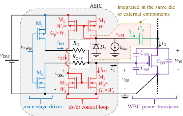
Fig. 1 shows a transistor-level diagram of the proposed method. A small value capacitor CS is used as a sensor of the derivative
of the voltage vDS. A capacitor with a high breakdown voltage is required, since it has to sustain the high voltage of the DC bus.
To amplify the current generated into this sensor during the dv/dt, a large bandwidth gain current mirror is proposed, which is the core idea for this method. The main challenge in this approach is to propose a circuit that can simultaneously supply a high amplitude feedback current with a very small time-delay response.
Typically, this feedback current iFB may be higher than 1 A, and the delay in the feedback loop should be lower than 1 ns. This
feedback current iFB is proportional to the derivative of the power transistor voltage vDS, current gain G and the value of the
capacitor CS acting as a dv/dt sensor (as shown in (2)). Typical CS values are much lower than the GaN CRSS, leading to CS in the
order of 0.7 pF to 2 pF. To reach these specifications, a CMOS integration with an optimal design is required. 𝑖FB= −𝐺 · 𝐶S
d𝑣DS
d𝑡 (2)
Fig. 1. Transistor-level schematic of the CMOS gate driver with a dv/dt feedback control loop for turn-on control.
Applying Kirchhoff’s law at the gate node, the dvDS/dt reduction is proportional to the feedback current iFB. The following
expression is obtained (valid as long as there is a current flowing through CS with iFB < iRG for stable operation, and a constant vM
voltage on the dv/dt sequence:
d𝑣DS d𝑡 = − 𝑣DRV−𝑣M 𝑅G𝐶GD + 𝑖FB 𝐶GD= − 𝑣DRV−𝑣M 𝑅G(𝐶GD+𝐺𝐶S) (3)
Note that the feedback circuit acts like an active equivalent gate-drain capacitor placed in parallel with CGD equal to G·CS.Due
on-chip. The feedback loop is composed of four low-voltage transistors, M1 to M4, and a high-voltage sensing capacitor CS. The
current buffer, also called the main stage driver, is composed of a PMOS transistor M5 and a NMOS transistor M6 used to source and sink the high gate currents, respectively. This buffer has a split output architecture, making it possible to use different resistors to adjust the turn-on and turn-off switching losses separately. The capacitors CGD, CGS and CDS are intrinsic to the GaN power
transistor. The diode DP is used only as a protection device at the input of the current mirror and is reverse biased during normal
operation. In case the current in CS is too high, the diode DP will clamp the vinM voltage at -0.7 V, preventing the gate voltage for
M1 and M2 will exceed more than the nominal maximum voltage value (5.5 V), therefore preventing breakdown destructive voltage in transistors M1 and M2.
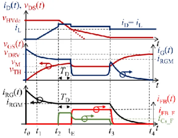
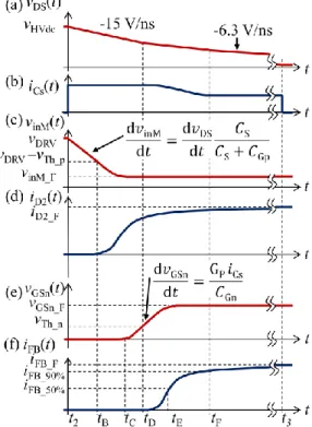
Fig. 2 introduces the waveforms for the main signals related to this approach that are used to actively control dv/dt. At the beginning of the dv/dt phase (at time t2), a delay TD is first required before the feedback loop starts to sink the current iFB. This
delay is mainly due to the settling time of the feedback loop circuit. The current iFB quickly reaches its final value iFB_F, which is
subtracted from the current iRG provided by the driver. When iFB_F increases, the gate current iG is decreased, leading to an increase
in time t3 in order to provide enough time to transfer the overall charge required by the gate of the power transistor during the
Miller plateau. As a result, the dvDS/dt is actively reduced. For the sake of simplicity, a constant Miller Plateau voltage was
considered.
Fig. 2. Theoretical waveforms showing the influence of the feedback loop time delay TD. iRGM is the current provided by the driver to the power transistor during the dv/dt event.
During the turn-off transition, the sensing capacitor CS sources (instead of sinking) a current that flows through the body diode
of M1. The width of M1 (W1) has to be sized correctly to handle the CS discharge current without breaking M1 or increasing the
voltage at node vinM too much.
It can be noted that if the total subtracted current iFB_F increases too much, due to a high loop gain and overly fast feedback
response, it can accidentally reach the value of the current supplied by the driver. In that case, the gate current iG in the power
device during the Miller plateau is cancelled. Then, the vDS and vGS voltages start to oscillate and the closed-loop system becomes
unstable. A limit of the method comes from the maximum amount of time TD required by the feedback current loop to operate. If
this time delay is higher than the duration t3 - t2 observed in open-loop, the turn-on transition will be missed, and the feedback loop
will have no effect on reducing dv/dt. It is important to ensure that the loop is able to operate as fast as possible. Finally, the time delay TD characterizes the system performance both in terms of time response and stability. In our case, we will optimize the
integration and circuit design to have less than 1 ns delay and to actively control initial fall time of 3 ns and above (dv/dtpeak =-175
B. Benefits of the Active Gate Driver
When designing a half bridge, there is a trade-off between the switching losses (EON, EOFF) and switching speed (dv/dt, di/dt).
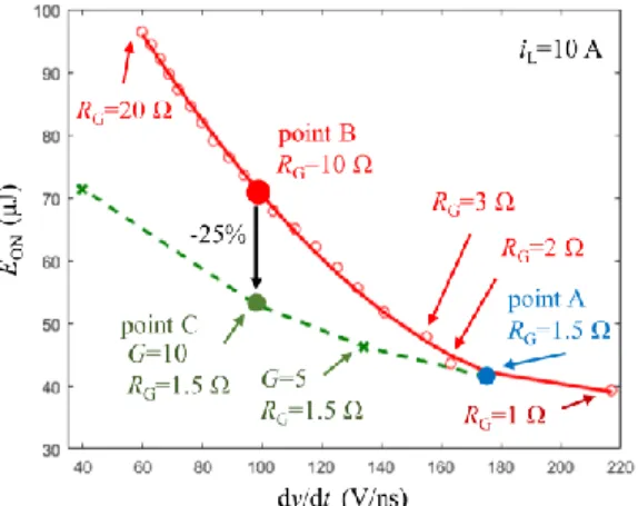
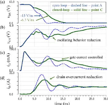
As long as the Miller effect is an active phenomenon (all turn-on or some turn-off transients at high load current), dv/dt is typically limited by the choice of the gate resistor RG. Fig. 3 introduces this classical trade-off (solid line) for the specifications detailed in
the next sections (obtained with a Cadence™ simulation with a model of a GS66508T GaN device). This work proposes to reduce the dv/dt leading from the point A to the point C (dashed line) but with fewer switching losses compared to a simple change in the gate resistor value RG (from point A to B). This change in the EMI-loss trade-off can be further dynamically tuned while changing
the AGD parameters.
Fig. 3. Trade-off EON vs dv/dt as a function of RG (solid line) or closed-loop gain G (dashed line) values for a constant bus voltage, load current and temperature. The proposed method aims to reach the point C without increasing the external gate resistor RG.
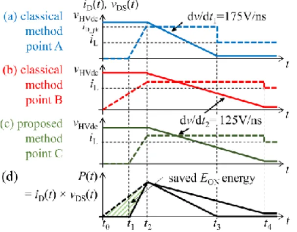
The amount of saved energy during turn-on is explained in Fig. 4. The proposed method reduces the amount of switching losses because the dv/dt value is reduced without modifying di/dt. As a consequence, the dissipated switching energy during the di/dt event (hatched area in Fig. 4 (d)) is canceled with our technique. The proposed method will not change di/dt because the proposed feedback loop will not be active during this phase. First, the di/dt value can be set by adjusting the value of RG, and then dv/dt can
be separately adjusted to reduce the negative effects of the EMI. One has to note that the parasitic stray inductance is neglected in this section of the paper (to explain the method), which is reasonable for high-frequency applications of GaN power transistors with optimal PCB designs (e.g., power loop stray inductances in the range of 1 nH). As a positive consequence, both points B and C (Fig. 3) will also generate a lower drain current overshoot during the dv/dt sequence [t4, t2] (Fig. 4) than point A; i.e., the dv/dt
Fig. 4. Waveforms with different values of dv/dt and di/dt for the operating points A, B and C. The saved energy is due to the reduction of dv/dt without changing di/dt.
C. Summary/Benchmark
The proposed method has several advantages compared to other methods used to control dv/dt.
--Compared to an added constant external capacitor CGD, the emulated capacitance G·CS will not affect the device immunity
through Miller coupling. The risk of a cross conduction fault is then mitigated. Another advantage is that the emulated capacitance can change through the feedback gain G. Moreover, the value of the required high-voltage CS capacitor can be reduced using our
technique; hence, its integration within the CMOS circuit is possible.
--Compared to open-loop techniques, the closed-loop method adapts the response for different systems and power devices under different conditions, while an open-loop approach would have to be designed for each different application and power device [27]. --Compared to other previously demonstrated closed-loop techniques, our approach is simple, extremely fast and highly integrated. While other closed-loop methods convert analog signals to digital signals using an ADC, their speed is limited to tens or hundreds of nanoseconds. Very high switching speeds and/or very short switching times cannot be controlled by the solutions presented today in the literature [10].
--Compared to other integrated solutions [28], [29], our solution offers both low (e.g., 48 V) and medium voltage (e.g., 400 V) applications, while using only low voltage CMOS devices and technology (e.g., 10 V, 20 V). Only a small (pF range) high-voltage sense capacitor is required, which is easily integrated with standard low-voltage CMOS technologies.
III. CMOSULTRA-FAST ACTIVE GATE DRIVER
The best way to implement the proposed method is by the use of an integrated analog circuit designed to minimize the delay TD
of the feedback loop, while allowing high gain and large feedback currents.
A. Overall design approach and CMOS Active Gate Driver performance
As introduced in Fig. 1, two stages of current mirrors are cascaded. Therefore, the total response time is defined by several consecutive phenomena.
This time delay results from a succession of several events. During the turn-on of the power transistor and the dv/dt sequence, the voltage vDS drops down from the voltage of the DC bus to a value close to zero. This transient is shown in Fig. 5(a). This signal, vDS(t), is the input signal of the feedback loop. Because the terminal vinM of the sensing capacitor CS is at a quasi-constant voltage
CS, the iCs(t) current, as shown on the second waveform Fig. 5(b). This current will charge the parasitic capacitor CGP present on
node vinM, involving the gates of the PMOS transistors M1 and M2, and change the biasing-voltage of the first current mirror, as
shown in Fig. 5(c). As soon as this voltage crosses the PMOS threshold voltage vTh_p, a current will start to flow through the channel
of M2, as shown in Fig. 5(d). This current charges the gates of the transistors M3 and M4, leading to an increase in the voltage
vGSn(t), as shown in Fig. 5(e). Finally, when vGSn reaches the NMOS threshold voltage vth_n, the output current iFB of the second
current mirror starts to rise, as shown in Fig. 5(f). As soon as this current iFB is no longer equal to zero, after time tD, the feedback
loop starts to operate and dv/dt is reduced and controlled.
Fig. 5. Waveforms for the voltages and currents of the current mirrors between times t2 and t3 (where CGp and CGn are respectively the total amount of parasitic capacitance viewed at the gate of M1 and M3). The feedback loop delay is detailed and expressed as TD(50%)=tE-t2.
In practice, the gain G of the feedback loop will vary according to the desired reduction in dv/dt. For instance, the higher the gain G is, the larger the iFB_F is, leading to a reduced dv/dt during turn-on. One can also note that tE will be larger when large gain
values G are set. Since the current mirror is composed of two stages, the gain G is the product of the two intermediate gains of each stage (Gp and Gn in Fig. 1). Based on simulations in Cadence™ with the design kit provided by the CMOS foundry, total
delay times tE-t2 in the range of 290 ps to 640 ps can be achieved (see Table II in [28] for more details). These values are functions
of the gain G, which is proportional to the sizes of the current mirror transistors, with lower gains leading to shorter delay times. Fig. 6(a) shows the dvDS/dt reduction for the system operating at point A (open-loop) and C (closed-loop), as defined in Fig. 3
and 4. Fig. 6(b) shows the extension of the Miller plateau due to the added virtual capacitance effect and closed-loop control. Fig. 6(c) shows the gate current iG that is going to the power device gate terminal, and Fig. 6(d) shows the drain current iD of the power
transistor and a beneficial reduction in overcurrent, while keeping the same initial di/dt.
A current biasing circuit is connected to the vinM node. Compared to the iCs amplitude, a small current is sinked from this node
that helps to precharge the intrinsic capacitances of the 4 transistors in the current mirrors, allowing a faster response. It should be noted that, in practice, both the feedback loop delay TD(50%) and its bandwidth are affected both by the sizing of the several
are the results of an optimization process involving both theoretical analysis and simulation validations using accurate CADENCETM SPECTRE transistor models of the CMOS technology.
Fig. 6. Simulation waveforms for (a) vDS, (b) vGS, (c) iG and (d) iD with (case C) and without (case A) the proposed method, including estimated PCB parasitic elements; (d) also shows a benefical effect of reduction in overcurrent (iD) during turn-on that is also provided by the proposed method. Case study for the 48 V application.
TABLEI
DIMENSIONING OF CMOS TRANSISTORS WIDTH
Type Key consideration to fix Width/Length M1 PMOS W1 fixed by minimum vinM voltage at
the highest iCs= Cs*Max(dvDS/dt), saturation regime
M2 PMOS W2=Gp × W1
M3 NMOS W3 is fixed to obtain vGSn=vdrv/2 for the highest iCs, saturation regime M4 NMOS W4=Gn × W3, where G=Gp × Gn
M5 PMOS W5 is fixed by the maximum source current for the GaN transistor, saturation regime
M6 NMOS W6 is fixed by the maximum sink current for the GaN transistor, saturation regime
*Note all PMOSs and NMOSs used have a vDSmax and vGSmax = 5 V and a length set to minimum.
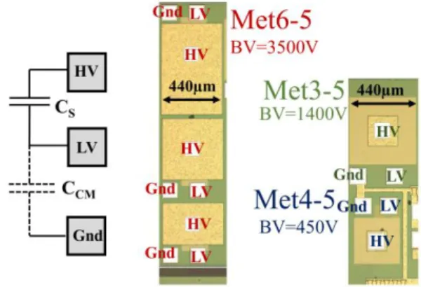
The CS sense capacitors are integrated with the CMOS AGD. Since CS must have a breakdown voltage higher than the GaN
power device, five different designs were considered that used different metal layers and inter layer dielectrics (Fig. 7). Integrated capacitance values of 0.7 pF, 1 pF and 1.5 pF have been implemented and tested. The breakdown characterization was performed under high vacuum, whereas the capacitance measurement was carried out with a HIOKI IM3570 using probe tips and calibration. As presented in Fig. 7, there is a common-mode parasitic capacitance between the LV node and the CMOS substrate that needs to be taken into consideration, which will add common mode current and a voltage divider effect to the sensing capacitor CS.
Fig. 7. Schematics and optical microscope pictures of the CMOS-integrated pF-range HV capacitors.
B. PCB Design
The analog circuits were implemented in 0.18 µm CMOS technology (AMS H18A6), and the fabricated test chip was packaged in a 6 mm × 6 mm QFN with 24 pins. Two PCB versions (Fig. 8) were realized with layout considerations to minimize the parasitic inductances of both the power and control loops of the power transistor. The PCB uses 4 layers for the prototypes for the EPC2001C transistors and 6 layers for prototypes with GS66508T transistors. Two low-voltage decoupling capacitors with a capacitance of 1 µF are placed close to the gate driver to supply the peak current required during the switching transients, in addition to decoupling the capacitors integrated on-chip. The sensing capacitor CS was integrated either on-chip or externally. Attention is made to
minimize the PCB parasitic capacitance between drain and source of the power device.
A CMOS gate driver was implemented for the low-side power transistor, while the gate of the high-side transistor was shorted to its source. The output power load is an air inductor with a low parasitic capacitance.
Please notice that our AGD topology can be adapted to any WBG power transistor, but due to the limit of vDS of integrated
current mirror and main buffer MOSFETs (5.5 V), the built prototype is limited to driving transistors from 0 to 5 V.
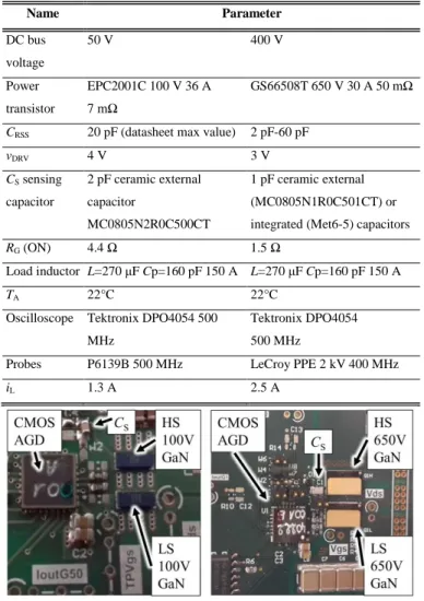
Consequently, this PCB is only used for double pulse tests with our CMOS AGD driving EPC GaN HEMTs or GaN System devices, with the active control implemented at the low-side transistor. Neither the drain nor the gate currents are probed to comply with extremely low parasitics both for the power loop and the driving loop. The parameters are summarized in Table II. In the case of GaN System devices, the gate driver supply voltage is not optimal to achieve a low ON-state resistance after turn-on. This result occurs due to the 5 V CMOS transistors used for M1 to M6 (Fig. 1), which were chosen for the first CMOS AGD prototype. Nonetheless, it is possible to drive such GaN devices under these conditions and to achieve a high switching speed, as demonstrated hereinafter.
C. Impact of the proposed method on the total gate charge
The emulated gate-to-drain capacitor (CGD+G·CS) leads to an extended Miller plateau, which will have an impact on the total
amount of gate charge provided by the gate driver supply. Since charge is subtracted during a turn-on event through transistor M4, the amount of charge required to turn-on the power device will increase. Indeed, in the proposed improved gate driver circuit, the amount of charge subtracted by the current mirror has to be provided by the driver power supply vDRV. This additional amount of
gate driver energy EDRV_SUP is given by:
𝐸DRV_SUP= 𝑣HVdc· 𝐺 · 𝐶S· 𝑣DRV (4)
Eq. (4) shows that the extra energy supplied by the driver will increase proportionally to the gain of the internal current feedback circuit G. A decrease of 58% (from -15 V/ns to -6.3 V/ns) in dvDS/dt will produce an increase of 58% in the energy provided by
the driver EDRV_SUP. Since the switching energy of the power device is considerably higher than the energy required by the driver,
this increase in driver energy has a limited impact. For the 400 V application, the gate charge is increased by 44% from point A to B. One can note that this additional gate driver energy is inherent to the proposed close-loop control, and other previously demonstrated approaches are subject to such an energy increase [20], [21].
TABLEII
TEST BENCH AND MEASUREMENT SETUP FOR EPC2001C AND FOR GS66508T
Name Parameter DC bus voltage 50 V 400 V Power transistor EPC2001C 100 V 36 A 7 mΩ GS66508T 650 V 30 A 50 mΩ
CRSS 20 pF (datasheet max value) 2 pF-60 pF
vDRV 4 V 3 V CS sensing capacitor 2 pF ceramic external capacitor MC0805N2R0C500CT 1 pF ceramic external (MC0805N1R0C501CT) or integrated (Met6-5) capacitors
RG (ON) 4.4 Ω 1.5 Ω
Load inductor L=270 μF Cp=160 pF 150 A L=270 μF Cp=160 pF 150 A
TA 22°C 22°C
Oscilloscope Tektronix DPO4054 500 MHz
Tektronix DPO4054 500 MHz
Probes P6139B 500 MHz LeCroy PPE 2 kV 400 MHz
iL 1.3 A 2.5 A
Fig. 8. Prototypes for a double-pulse test-bench with the proposed dv/dt control circuit.
D. Application to a 100 V GaN power commutation cell
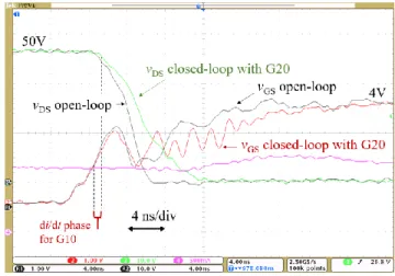
Using the fabricated CMOS AGD with the integrated buffer, Fig. 9 shows experimental waveforms obtained during the turn-on with and without the closed-loop control, with the same gate resistor and driving voltages for the same test parameters as previously described in Table II. For the closed-loop, a prebiasing current of 20 µA was applied at the input of the current mirror (vinM node)
using a sourcemeter unit Keithley 2612B. Without the closed-loop control, the fall time is 4.36 ns (90%-10% vDS(t)), with a peak
dv/dt of -15 V/ns. Even with this fast switching event, the AGD is able to actively control the dv/dt sequence from the beginning, without modifying di/dt. It is possible to see the di/dt sequence in the vGS signals because it is the interval between vTH (around 1.7
V from the datasheet) and the beginning of the dv/dt phase, the second line marked in Fig. 9. The iL is not measured in our circuit
to reduce the power loop inductance. However, the vGS(t) signal with and without the closed-loop control clearly shows that the
reduced dv/dt with the closed-loop feedback allows the reduction of the drain current overshoot and subsequent gate overvoltage before the Miller plateau. Due to the AGD, the fall time is increased from 4.36 ns to 7.37 ns (90%-10% vDS) without affecting the
gate charge before the Miller plateau. This increase in fall time corresponds to the reduction in peak dvDS/dt from 15 V/ns to
-6.3 V/ns as shown in Fig. 7. One must note that all the analog circuits are integrated within the CMOS AGD; only the driver supply decoupling capacitors, HV-sensing capacitor (for some tests) and gate resistors are external devices. It should also be emphasized that due to the high speed and large gain of the integrated current mirrors, the HV-sensing capacitor CS is designed in the pF range,
allowing its further integration within the CMOS chip (please see table II for values).
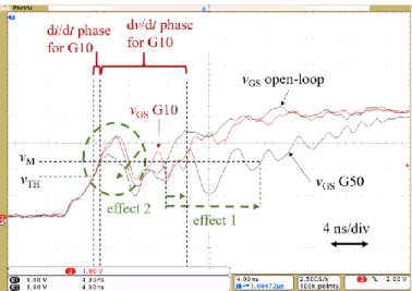
Fig. 10 shows the measured vGS waveforms in open-loop and in closed-loop with gains of 10 and 50 for the same value of sensing
capacitor CS = 2 pF (external). The duration of the Miller plateau is successfully increased with higher feedback gain values (“effect
1” in Fig. 10). It is also clear that the diD/dt phase is not affected by the closed-loop control. The di/dt value is estimated to be
approximately 1A/ns, since the vGS signal changes from vTH to vM in approximately 1 ns. Please note that measurements are carried
out with iL=2 A to obtain higher values of dv/dt to explore the speed limits of the method. In addition to the reduction of the dvDS/dt
with higher closed-loop gains, the drain overcurrent during turn-on is also reduced. This effect can be seen in Fig. 10 (“effect 2”) where iD(t) and vGS(t) are linked by the transconductance of the GaN transistor in this operation state. Reducing the drain
overcurrent and gate overvoltage before the Miller plateau is a clear proof of the ultrafast closed-loop control. Due to the AGD, the classical design trade-offs in operating conditions and reliability issues are clearly pushed forward.
Fig. 9. Measured vDS(t) and vGS(t) waveforms for open-loop (without the proposed method) and closed-loop (with the proposed method) controls.
To compare the implementation of the AGD with a gain of 50, Fig. 11 shows a comparison between the experimental results and simulated waveforms. Increasing the feedback gain of the current mirrors decreases dvDS/dt while maintaining an identical
Fig. 10. Measured vGS(t) for open-loop (without the proposed method) and closed-loop controls with mirror gains equal to 10 and 50.
Fig. 11. Measured and simulated waveforms vDS(t) and vGS(t) for open-loop and closed-loop controls using a current mirror with gain of G=50. A prebiasing current of 150 μA is used in this measurement.
E. Application to a 650 V GaN power commutation cell
Fig. 12 shows the implementation of our technique with a GaN System transistor GS66508T for gain G=10 and CS=1 pF. The
fall time during turn-on (vDS, 90% to 10%) is increased from 3.3 ns (openloop) to 8 ns (closedloop). The peak dv/dt value of
-175 V/ns is therefore reduced to -120 V/ns with our CMOS AGD. A biasing current of 320 µA is applied, and one can observe that dv/dt starts to be attenuated in less than 1 ns. All the parameters for the results are described in Table II. Without an integrated analog feedback loop, such a result would not be possible. This experimental result shows, for the first time, the active control of 650 V GaN devices with extremely high switching speeds, both in open- and closed-loops. Fig. 13 shows a similar result, where the high-voltage capacitor is integrated on the same CMOS chip as the gate driver (1 pF, 3.5 kV breakdown, see section IV). The small differences in switching speeds between Fig. 12 and Fig. 13. can be explained by the use of a different PCB board, albeit from the same design (typical dispersion in power devices, CMOS gate driver and PCB parasitics). Nonetheless, this result clearly shows that the AGD can be fully functional, even with the high-voltage sense capacitor CS monolithically integrated within the
Fig. 12. Measured vDS(t) waveforms for open-loop (without the proposed method) and closed-loop (with the proposed method) controls for 650 V GS66508T GaN transistors. ibias=320 µA.
Please note that the effect of a biasing current improving the feedback response time can be seen comparing Fig. 12 (ibias=320 µA) and Fig. 13 without biasing current. The attenuation in dv/dt occurs latter in Fig. 13 compared to Fig. 12, as predicted
and discussed before.
Fig. 13. Measured vDS(t) waveforms with an embedded sensing capacitor CS and without an ibias current for this measurement.
F. Benefits for the EON vs. dv/dt trade-off
Table III shows the simulated values in Cadence™ related to the points presented in Fig. 3 and Table II according to the experimental results obtained with the closed-loop systems. EON is calculated by simulations using the SPICE-compatible model
of the transistor provided by the manufacturer for each GaN power device. Comparing points A, B and C, the maximum value of dvDS/dt was reduced by 61% with our technique, while increasing EON by only 46% (point C, closed-loop), whereas it would have
increased by 100% with a larger gate resistor (point B) for the same dvDS/dt. This balance sheet must be further confirmed by EON
measurements in our prototype. In this work, the drain current of the GaN transistor was not measured, as it would have increased the power loop parasitic inductance and therefore limited our capability to show a very fast active gate control.
G. Effect of the closed-loop control in the frequency domain
The experimental data for vDS(t) for the turn-on, turn-off, ON and OFF-states measured with the double pulse method are merged
into a periodic signal, with a 1 MHz switching frequency and a duty cycle of 0.5. The Fourier transform of such a vDS(t) signal is
shown in Fig. 14 and Fig. 15 for 48 V and 400 V applications, respectively, for both the open-loop and closed-loop controls. An analytical expression for the expected attenuation KdB(G20) at high frequency is provided by (5). Consequently, for the reduction in
the peak dv/dt during turn-on with the closed-loop control, the vDS spectrum is reduced at high frequency, e.g., 13 dBµV lower at
100 MHz (48 V application, Fig. 14) or 7.6 dBµV at 100 MHz (400 V application, Fig. 15). This is a clear advantage of the AGD for reducing the high-frequency voltage content of the switching nodes with fewer switching losses compared to a classical adjustment of the gate resistor.
𝐾dB(G20)= 40𝑙𝑜𝑔 (
𝑑𝑣/𝑑𝑡(𝐺20)
𝑑𝑣/𝑑𝑡(𝑂𝐿)) (5)
Fig. 14. vDS spectrum with open and closed-loop during turn-on calculated from data measured for the EPC transistor with all the parameters in Table II.
IV. CONCLUSION
While the typical fall times for GaN HEMTs are as low as a few nanoseconds in 48 V and 400 V applications, it is quite challenging to achieve a closed-loop feedback from the high-
TABLEIII
SIMULATED EON IN OPEN AND CLOSED-LOOP
FOR TWO DIFFERENT GAN VOLTAGE-RANGE APPLICATIONS
iL=1 A
100 V GaN EPC2001C tests at 50 V G×Cs=20 pF 650 V GaN GS66508 tests at 400 V G×Cs=20 pF Point* RG (Ω) EON (µJ) |𝐝𝒗/𝐝𝒕| (V/ns) RG (Ω) EON (µJ) |𝐝𝒗/𝐝𝒕| (V/ns) A B C 4.4 22 4.4 1.42 1.845 (+30%) 1.62 (+16.1%) 15 4.715 (-68%) 4.67 (-68%) 1.5 10 1.5 18.18 19.62 (+7.9%) 18.81 (+3.4%) 175 97 (-44%) 97 (-44%) iL=20 A Point* RG (Ω) EON (µJ) |𝐝𝒗/𝐝𝒕| (V/ns) RG (Ω) EON (µJ) |𝐝𝒗/𝐝𝒕| (V/ns) A B C 4.4 16.6 4.4 5.488 12.42 (+126%) 11.51 (+110%) 14 5.189(-63%) 5.163(-63%) 1.5 13 1.5 60.88 122.2(+100%) 89.14(+46%) 119 46 (-61%) 46 (-61%) *Similar points as defined in Fig. 3 and Fig. 4 for peak dv/dt values.
Fig. 15. vDS spectrum with open and closed-loop during turn-on calculated from data measured for the GaN Systems 650 V transistor with all the parameters in Table II.
voltage drain to the low-voltage gate node. In this context, an ultrafast method to actively control the dv/dt rate of the GaN HEMT drain-source voltage during turn-on is proposed and experimentally demonstrated. The key challenges are to achieve a subnanosecond delay for the feedback loop and to integrate all active and passive devices within a CMOS gate driver. Here, a CMOS AGD was designed, characterized and further implemented with 100 V and 650 V GaN transistors.
The CMOS AGD is based on a standard low-voltage CMOS technology. Due to the AGD, the dv/dt sequence can be actively tuned, without modifying the di/dt sequence. The Miller plateau is then extended, with benefits on reliability consideration with a lower capacitive drain overcurrent and gate overvoltage during the active gate driving. Compared to classical methods (e.g., fixed or variable gate resistors), switching losses are reduced for the same level of dv/dt reduction. The AGD showed a clear reduction in the peak dv/dt in 400 V and 48 V applications from -175 V/ns to -120 V/ns and from -15 V/ns to -6.3 V/ns, respectively.
To achieve this active control with extremely fast GaN devices, the response time of the feedback loop ranges between 290 ps and 640 ps (gain and bias dependent). Since the technique used here is based on the use of active devices, the feedback gain can be further adapted to comply with system-level considerations (e.g., best trade-off between switching losses vs. EMI). As a future work, EMI radiative measurements will be considered to confirm the benefits of the AGD.
V. APPENDIX
Fig. 16 and Fig 17 shows that the system proposed in this paper will not affect the turn-off behavior because the discharge current of CS will pass through the body diode of M1. Fig. 18 shows the feedback loop delay measured by connecting the current
mirror input to the drain of the power device (for normal operation) and its output to a 14.7 Ω resistor to vDRV. The potential at the
output of the current mirror (M4 Drain potential) is referred to as vout_M in the figure.
ACKNOWLEDGMENTS
The authors would like to thank B. Lantin, D. Flumian, S. Vinnac, M.L. Locatelli and S. Dinculescu from Laplace lab for their contribution to the experimental results.
Fig. 16. Measured vDS(t) and vGS(t) waveforms for open-loop (without the proposed method) and closed-loop (with the proposed method) for a turn-off event (case EPC2001C vHVdc =50 V).
Fig. 17. The behavior of the system during the turn-off event. (a) Theoretical waveforms during turn-off, (b) the discharge path of CS capacitor during turn-off event and (c) simulation showing the feedback system will not source a current (iFB) during a turn-off event.
REFERENCES
[1] A. Bindra, "Wide-Bandgap Power Devices: Adoption Gathers Momentum," in IEEE Power Electronics Magazine, vol. 5, no. 1, pp. 22-27, March 2018. [2] T. Keim, "ECCE 2017 Explores Electrification of Aircraft [Society News]," in IEEE Power Electronics Magazine, vol. 5, no. 1, pp. 60-64, March 2018. [3] Trade-ofF. Gao, Q. Zhou, P. Wang and C. Zhang, "A Gate Driver of SiC MOSFET for Suppressing the Negative Voltage Spikes in a Bridge Circuit," in IEEE
Trans. Power Electron., vol. 33, no. 3, pp. 2339-2353, March 2018.
[4] Zhang, J. Dix, F. F. Wang, B. J. Blalock, D. Costinett and L. M. Tolbert, "Intelligent Gate Drive for Fast Switching and Crosstalk Suppression of SiC Devices," in IEEE Trans. Power Electron., vol. 32, no. 12, pp. 9319-9332, Dec. 2017.
[5] T. Kim, D. Feng, M. Jang and V. G. Agelidis, "Common Mode Noise Analysis for Cascaded Boost Converter With Silicon Carbide Devices," in IEEE Trans. Power Electron., vol. 32, no. 3, pp. 1917-1926, March 2017.
[6] P. Nayak and K. Hatua, "Active Gate Driving Technique for a 1200 V SiC MOSFET to Minimize Detrimental Effects of Parasitic Inductance in the Converter Layout," in IEEE Transactions on Industry Applications, vol. 54, no. 2, pp. 1622-1633, March-April 2018.
[7] A. P. Camacho, V. Sala, H. Ghorbani and J. L. R. Martinez, "A Novel Active Gate Driver for Improving SiC MOSFET Switching Trajectory," in IEEE Transactions on Industrial Electronics, vol. 64, no. 11, pp. 9032-9042, Nov. 2017.
[8] P. Nayak and K. Hatua, "Parasitic Inductance and Capacitance-Assisted Active Gate Driving Technique to Minimize Switching Loss of SiC MOSFET," in IEEE Transactions on Industrial Electronics, vol. 64, no. 10, pp. 8288-8298, Oct. 2017.
[9] S. Acharya, X. She, F. Tao, T. Frangieh, M. H. Todorovic and R. Datta, "Active gate driver for SiC MOSFET based PV inverter with enhanced operating range," 2018 IEEE Applied Power Electronics Conference and Exposition (APEC), San Antonio, TX, 2018, pp. 3230-3237.
[10] M. V. Krishna and K. Hatua, "Closed loop analog active gate driver for fast switching and active damping of SiC MOSFET," 2018 IEEE Applied Power Electronics Conference and Exposition (APEC), San Antonio, TX, 2018, pp. 3017-3021.
[11] H. C. P. Dymond, D. Liu, J. Wang, J. J. O. Dalton and B. H. Stark, "Multi-level active gate driver for SiC MOSFETs," 2017 IEEE Energy Conversion Congress and Exposition (ECCE), Cincinnati, OH, 2017, pp. 5107-5112.
[12] Y. Yang, Y. Wang and Y. Wen, "An active gate driver for improving switching performance of SiC MOSFET," 2018 7th International Symposium on Next Generation Electronics (ISNE), Taipei, 2018, pp. 1-4.
[13] A. Tripathi, K. Mainali, S. Madhusoodhanan, A. Yadav, K. Vechalapu and S. Bhattacharya, "A MV intelligent gate driver for 15kV SiC IGBT and 10kV SiC MOSFET," 2016 IEEE Applied Power Electronics Conference and Exposition (APEC), Long Beach, CA, 2016, pp. 2076-2082.
[14] H. Ghorbani, V. Sala, A. Paredes and J. L. Romeral, "A simple gate drive for SiC MOSFET with switching transient improvement," 2017 IEEE Industry Applications Society Annual Meeting, Cincinnati, OH, 2017, pp. 1-6.
[15] D. Brain Ma, "Driving GaN Power Transistors," 2019 IEEE 31th International Symposium on Power Semiconductor Devices and ICs (ISPSD), Shanghai, 2019, pp. 87-90.
[16] D. Reusch and M. de Rooij, "Evaluation of gate drive overvoltage management methods for enhancement mode gallium nitride transistors," 2017 IEEE Applied Power Electronics Conference and Exposition (APEC), Tampa, FL, 2017, pp. 2459-2466.
[17] E. Velander et al., "An Ultralow Loss Inductorless dv/dt Filter Concept for Medium-Power Voltage Source Motor Drive Converters With SiC Devices," in IEEE Trans. Power Electron., vol. 33, no. 7, pp. 6072-6081, July 2018.
[18] V. D. Santos, B. Cougo, N. Roux, B. Sareni, B. Revol and J. Carayon, "Trade-off between losses and EMI issues in three-phase SiC inverters for aircraft applications," 2017 IEEE International Symposium on Electromagnetic Compatibility & Signal/Power Integrity (EMCSI), Washington, DC, 2017, pp. 55-60.
[19] D. Colin and N. Rouger, "High speed optical gate driver for wide band gap power transistors," 2016 IEEE Energy Conversion Congress and Exposition (ECCE), Milwaukee, WI, 2016, pp. 1-6.D.
[20] Shihong Park and T. M. Jahns, "Flexible dV/dt and di/dt control method for insulated gate power switches," in IEEE Transactions on Industry Applications, vol. 39, no. 3, pp. 657-664, May-June 2003.
[21] B. Sun, R. Burgos, X. Zhang and D. Boroyevich, "Active dV/dt control of 600V GaN transistors," 2016 IEEE Energy Conversion Congress and Exposition (ECCE), Milwaukee, WI, 2016, pp. 1-8.
[22] Y. Wen, M. Rose, R. Fernandes, R. Van Otten, H. J. Bergveld and O. Trescases, "A Dual-Mode Driver IC With Monolithic Negative Drive-Voltage Capability and Digital Current-Mode Controller for Depletion-Mode GaN HEMT," in IEEE Trans. Power Electron., vol. 32, no. 1, pp. 423-432, Jan. 2017.
[23] P. Choi, U. Radhakrishna, C. Boon, D. Antoniadis and L. Peh, "A Fully Integrated Inductor-Based GaN Boost Converter With Self-Generated Switching Signal for Vehicular Applications," in IEEE Trans. Power Electron., vol. 31, no. 8, pp. 5365-5368, Aug. 2016.
[24] Y. Zhang, M. Rodríguez and D. Maksimović, "Very High Frequency PWM Buck Converters Using Monolithic GaN Half-Bridge Power Stages With Integrated Gate Drivers," in IEEE Trans. Power Electron., vol. 31, no. 11, pp. 7926-7942, Nov. 2016.
[25] (ECCE), Milwaukee, WI, 2016, pp. 1-6.Application notes GN001 “Design with GaN Enhancement mode HEMT” https://gansystems.com/wp-content/uploads/2018/02/GN001 Design_with_GaN_EHEMT_180228-1.pdf
[26] Y. Chen, X. Ke and D. B. Ma, "A 10MHz 5-to-40V EMI-regulated GaN power driver with closed-loop adaptive Miller Plateau sensing," 2017 Symposium on VLSI Technology, Kyoto, 2017, pp. C120-C121.M. Blank, T. Glück, A. Kugi and H. Kreuter, "Digital Slew Rate and S-Shape Control for Smart Power Switches to Reduce EMI Generation," in IEEE Trans. Power Electron., vol. 30, no. 9, pp. 5170-5180, Sept. 2015.
[27] H. C. P. Dymond et al., "A 6.7-GHz Active Gate Driver for GaN FETs to Combat Overshoot, Ringing, and EMI," in IEEE Trans. Power Electron., vol. 33, no. 1, pp. 581-594, Jan. 2018.
[28] Y. Wen, M. Rose, R. Fernandes, R. Van Otten, H. J. Bergveld and O. Trescases, "A Dual-Mode Driver IC With Monolithic Negative Drive-Voltage Capability and Digital Current-Mode Controller for Depletion-Mode GaN HEMT," in IEEE Transactions on Power Electronics, vol. 32, no. 1, pp. 423-432, Jan. 2017. [29] J. Chen et al., "A Smart IGBT Gate Driver IC With Temperature Compensated Collector Current Sensing," in IEEE Transactions on Power Electronics, vol.
34, no. 5, pp. 4613-4627, May 2019.
[30] P. Bau, M. Cousineau, B. Cougo, F. Richardeau, S. Vinnac, D. Flumian, and N. Rouger, "Sub-Nanosecond Delay CMOS Active Gate Driver for Closed-Loop dv/dt Control of GaN Transistors," 31st International Symposium on Power Semiconductor Devices and ICs (ISPSD), pp. 75-78, 2019.