HAL Id: hal-02991788
https://hal.archives-ouvertes.fr/hal-02991788
Submitted on 16 Nov 2020
HAL is a multi-disciplinary open access
archive for the deposit and dissemination of
sci-entific research documents, whether they are
pub-lished or not. The documents may come from
teaching and research institutions in France or
abroad, or from public or private research centers.
L’archive ouverte pluridisciplinaire HAL, est
destinée au dépôt et à la diffusion de documents
scientifiques de niveau recherche, publiés ou non,
émanant des établissements d’enseignement et de
recherche français ou étrangers, des laboratoires
publics ou privés.
Single plasmon spatial and spectral sorting on a
crystalline two-dimensional plasmonic platform
Upkar Kumar, Sreenath Bolisetty, Raffaele Mezzenga, Christian Girard, Erik
Dujardin, Aurelien Cuche
To cite this version:
Upkar Kumar, Sreenath Bolisetty, Raffaele Mezzenga, Christian Girard, Erik Dujardin, et al.. Single
plasmon spatial and spectral sorting on a crystalline two-dimensional plasmonic platform. Nanoscale,
Royal Society of Chemistry, 2020, 12 (25), pp.13414-13420. �10.1039/D0NR02066D�. �hal-02991788�
Jour
nal
Name
Single plasmon spatial and spectral sorting on a crystalline
two-dimensional plasmonic platform
†
Upkar Kumar,a Sreenath Bolisetty,b Raffaele Mezzenga,b Christian Girard,a Erik Dujardin,a
and Aurélien Cuche∗a
In the context of the emerging field of quantum plasmonics, we demonstrate in this manuscript the wavelength-dependent propagation and sorting of single plasmons launched in a two-dimensional crystalline gold flake by a broadband quantum nanoemitter. The stream of single plasmons in the visible is produced by a nanodiamond hosting a single nitrogen-vacancy color center positioned in the near field of the mesoscopic metallic microplatelet. Spatially and spectrally resolved images of the single plasmon propagation in the pristine hexagonal flake, and then in the same structure after insertion of a Bragg mirror, are obtained by filtered image-plane acquisitions on a leakage-radiation microscope. Our work on two-dimensional crystalline structures paves the way to future fundamental studies and applications in quantum plasmonics.
1
Introduction
When an electromagnetic wave impinges on the interface be-tween a noble metal and a dielectric material under specific con-ditions, charge density oscillations can be excited1,2. These sur-face waves, known as sursur-face plasmon (SP) polaritons, allow for subwavelength confinement and large field enhancement in the near field. Recently, several groups have extended this field of research in the quantum regime with the observation of quan-tum signatures in optical systems using plasmons3–5. These early works can be classified in three different groups depending on the light source considered and the experimental configurations.
First, far-field indistinguishable photons generated, for in-stance, by semiconductor quantum dots at low temperature can be coupled to SPs. The observation of coalescence6,7 or anti-coalescence8 phenomena in plasmonic beam splitters has ev-idenced the Hong-Ou-Mandel effect for two-plasmon interfer-ences. Secondly, far-field entangled photon pairs generated by conservation rules in pumping non-linear crystals can be cou-pled to thin nanostructured plasmonic metal films9,10 or stripe-like plasmonic guides11to investigate the effect of Ohmic losses on the coherence of the system. One key asset of entangled photon-plasmon pairs is to allow quantum sensing experiments with higher sensitivities than conventional approaches12–14. At last, nanometric single photon sources, such as quantum dots,
a
CEMES, University of Toulouse and CNRS (UPR 8011), 29 rue Jeanne Marvig, BP 94347, 31055 Toulouse, France; E-mail: [email protected]
bETH Zurich, Department of Health Sciences and Technology, Schmelzberg-strasse 9,
CH-8092 Zurich, Switzerland.
† Electronic Supplementary Information (ESI) available: See DOI: 00.0000/00000000.
molecules or colored centers in nanocrystals, can be directly po-sitioned in the near-field of plasmonic structures where they de-liver a stream of single photons. This integrated approach suc-cessfully demonstrated the excitation of single plasmons17,18and single plasmon interferences19. These point-like photon “guns” are sensitive to their direct environment and their photodynamics is driven by the local modification of the field distribution and/or density of available states15,16, leading to strategies for density of states mapping to identify the best coupling locations20,21.
Fig. 1 (a) Artistic view of a single photon emitter coupled to a two-dimensional gold flake. (b) Second-order correlation function of a NV− center hosted by the nanodiamond coupled to the gold flake. (c) SEM image of the crystalline micrometric gold flake before the cleaning step. The inset shows a magnified SEM image of the nanodiamond hosting the single NV center presented in (b). (d) Scheme of the confocal lumi-nescence microscope with an excitation wavelength at λ =532 nm (BP: Bandpass filter; PH: Pinhole).
In spite of inherent losses in metallic structures, quantum ef-fects are thus observed in plasmonics devices, which offer a unique route towards on-chip quantum control. A first genera-tion of integrated quantum optical components operated in the single plasmon regime have been successfully demonstrated by coupling a local single photon nanosources to punctual (0D)4,16 and unidimensional (1D)4,22,23 SP channels. For instance, the realization of logical operations24or the plasmon-mediated cou-pling between two quantum emitters25have been achieved. Yet, these systems do not offer enough spatial degrees of freedom for the design of actual devices. For instance, the optical interconnex-ion of qbits in planar architectures will require mesoscale multi-inputs/outputs 2D platforms.
In this work, we report on the spatial and spectral sorting of single plasmons excited by a quantum emitter on a 2D microscopic crystalline gold flake in the visible range. The broadband optical signal emitted one photon at a time from the embedded Nitrogen-Vacancy (NV) source is transferred by the continuum of available SP modes along the flake, where the spectral sorting is obtained by the damping during propagation and by the interaction with a nanofabricated hole array. This periodic structure reveals the trajectories of the single plasmons and redistributes the optical signal in 2D towards the output ports as a function of wavelength. Our study demonstrates the potential of crystalline gold flakes as multi-inputs/outputs 2D platforms for future developments in quantum plasmonics.
2
Results and discussion
Figure 1(a) shows a quantum emitter located at the edge of an 8-µ m diameter hexagonal gold crystalline flake. The second-order correlation function (g(2)(τ)) of the nanodiamond targeted in this work is presented in Figure 1(b). It is characteristic of a single NV− in diamond with a clear signature of photon antibunching at zero delay below 0.5, ensuring the emission of a single photon per cycle.
This configuration has been obtained by co-deposition of a solu-tion of nanodiamonds (mean size: 80 nm) and a colloidal suspen-sion of micrometric crystalline gold flakes (thickness: 40 nm) on a cross-marked ITO-covered glass substrate (Figure 1(c))26. With this approach, the NDs are preferentially positioned along the edges of the flakes. Such crystalline plasmonic flakes are offering a low scattering loss alternative to amorphous metal films27,28. They can be equally patterned on-demand by ion29or electron beam lithography32 as reported in several studies on antenna, waveguides29–32, modal engineering33or single photon emission enhancement34. In order to obtain a satisfactory compromise be-tween delocalization of the signal and propagation losses, a lat-eral size in the 3-10 µm range has been targeted.
We study the nanodiamond-flake system presented in Figure 1(c) by confocal luminescence microscopy coupled to a leak-age radiation microscopy detection scheme as sketched in Figure 1(d). A linearly polarized cw excitation laser at λL=532 nm is fo-cused on the sample with a x100 high numerical aperture immer-sion objective (NA=1.3). The luminescence from the sample, po-sitioned on a xy piezoscanner, is collected through a dichroic
mir-ror centered at λL=550 nm. For a given position of the excitation spot, the acquisition is performed either on a sensitive EMCCD camera (Andor Ixon 3) with a bandpass filter (λc=692±40 nm) for the image plane snapshots, or through a 75-µm pinhole on a CCD camera (Andor Newton DU920P-BVF) coupled to spectrom-eter (Andor Shamrock 303i) with a 300-grooves-per-mm grating and a longpass filter (λl p=600 nm). For off-axis acquisition, the pinhole can be moved in a conjugated xy plane.
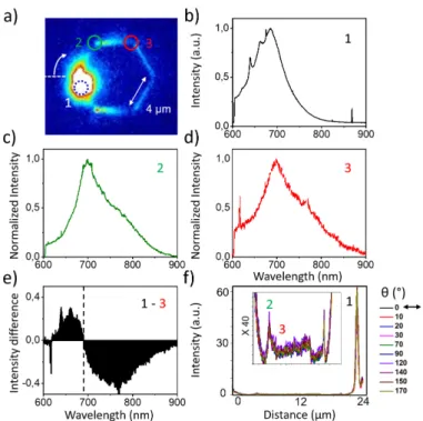
Fig. 2 (a) Leakage luminescence image of the SP signal propagation in two-dimensional gold flake integrated over the entire NV−spectrum. (b-d) Luminescence spectra from the NV−center acquired (b) directly on the nanodiamond in position 1, (c) at the corner labeled 2 in (a), (d) at a second corner labeled 3 in (a). The spectra are normalized with respect to their maximum slightly below 700 nm. (e) Difference between the normalized spectra in 3 and 1 (reference) as a function of the wavelength emphasizing the spectral redistribution of the signal after propagation. (f) Luminescence signal along the perimeter of the gold flake as a function of the incident polarization. A zoom (x40) of the signal in the central region is shown in inset, where the positions 1,2 and 3 are indicated too.
In Figure 2(a), the experimental luminescence map shows the bright emission of the nanodiamond in position 1 but also light scattering at the edges of the hexagonal flake with an intensity decreasing with the distance to the photon source. Figure 2(b) shows the normalized spectrum of the signal directly recorded on the nanodiamond at position 1. It corresponds to the broadband emission of a NV−, with a residual luminescence from gold (see SI), which will be used as an internal reference in the following discussion. More interestingly, the edge-scattered signal recorded at remote locations (positions 2 and 3 in Figure 2(a)), microm-eters away from the nanodiamond source, retains the signature of the NV−with lower amplitude, a redshift of the peak position (∆λ ≈ 15 nm) and a slightly altered global shape (Figure 2(c) and (d)). The evolution of the intensity is highlighted in Fig-ure 2(e) where the spectrum acquired in position 3 is subtracted
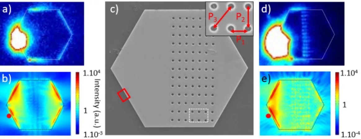
Fig. 3 Experimental (a) and simulated (b) SP signal transfer maps in the two-dimensional gold flake integrated over the entire NV−spectral window. In the simulated map, the position of the dipolar emitter is indicated by a red dot. (c) SEM image of the gold flake after cleaning and FIB milling of a hole array. The red square indicates the position of the nanodiamond under study. The relevant geometrical parameters of the array are shown in inset, which corresponds to the white rectangle in the main image. (d)-(e) Same as (a) and (b) for the structure with the hole array displayed in (c).
to the reference spectrum 2(b). Both spectra are normalized to their maximum intensity. Far from the source, the longest wave-lengths clearly outperform the sub-700 nm emission as can be expected from a wavelength-dependent damping during SP prop-agation at the metal-air interface. As a consequence, a turning point is clearly visible in Figure 2(e) (indicated by the vertical black dashed line). Indeed gold has interband transitions that mainly occur for wavelengths below 600 nm, the imaginary part of the dielectric function thus increases in this spectral window resulting in a stronger absorption at shorter wavelengths. Inter-estingly, the signal recorded exhibits no polarization-dependance. In Figure 2(e), crosscuts of the luminescence intensity along the perimeter of the flake are shown as a function of the incident polarization. The different curves overlap and do not show any significant intensity redistribution as the polarization of the laser is rotated. This suggests that the transition dipole of the single NV center is oriented along the z axis. Although a z-oriented dipole would hardly be excited by a polarization lying in the xy plane, the high numerical aperture used as well as the local redistribu-tion of the electric field by the edge of the gold microplatelet (see SI) might explain the effective excitation of the NV. In the follow-ing, the polarization of the incident beam has therefore been kept at 0◦(along the x-axis).
To compute the energy transfer between the NV center and the gold flake, we have performed numerical simulations of the lo-cal electric field above the microplatelet based on the 3D Green Dyadic Method (GDM) as described in earlier reports35. We con-sider that the emitting quantum system behaves like a fluctuating dipole oscillating at the ω0frequency:
mNV(t) = µ12u cos(ω0t) (1) where µ12 is the dipolar electric transition moment oriented along the unit vector u. In turn, this dipole excites the plasmon modes of the gold crystal that can be characterized by the electric field E(r, t) =1 2 n E(r, ω0)e−iω0t+ c.c. o (2) with E(r, ω0) = µ12S(r, r0, ω).u (3) where S(r0, r, ω) is the field susceptibility of the sample (gold plate + surface).
The comparison between the experimental wide-field lumines-cence and simulated maps is presented in Figure 3(a). In our experiments, the collected intensity accumulates the response of the plasmonic platform under the repeated excitation by trains of single photons generated by the broadband single photon NV source. Our simulations support this broadband coupling since the map presented in Figure 3(b) is the incoherent sum of five maps computed at 600, 650, 700, 750 and 800 nm. In addition, each simulated map is the average over three simulated maps for dipolar sources oriented along the x, y and z-axis to account for the uncertainty on the orientation of the NV dipole (the individ-ual maps for each dipole orientation are presented in the SI). In-terestingly, the significant intensity of the recorded luminescence shows that such a localized quantum source is powerful enough to drive the classical plasmon mode response in the macroscopic gold flake.
Most of the scattered signal in experimental and simulated maps is observed along the edges of the flake. Similarly, the intensity of the signal vanishes as the distance to the launching point increases. The comparison in Figures 3(a,b) strongly sug-gests that the remote signal observed in experiments is mediated by SPs. Figure 3 reveals small differences between simulated and acquired maps. Although near-field simulated maps cannot be di-rectly compared to the far-field experimental images, we attribute the main deviations observed in the distribution of the signal to the imperfect mesh model of the structure used in the simulation. Nevertheless, the general good agreement between acquired and simulated maps should be pointed out. In order to reveal the path of the single SPs launched by the quantum emitter, we have carved a hole array in the flake by focused ion beam (FIB). This hole array has the following features: the three periods indicated in the inset are P1=392 nm, P2=500 nm, P3=635 nm, and the
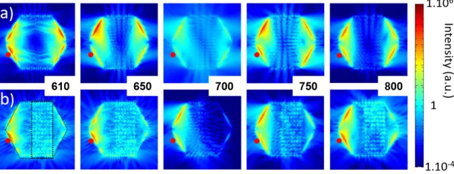
Fig. 4 (a) Serie of wide-field luminescence images acquired at five different wavelentghs on the pristine flake. From left to right: bandpass filters are centered at λBP= 610, 650, 700, 750 and 800 nm. The white arrow indicates the laser polarization at 0◦. (b) Schematic of the flake with the input/output nomenclature considered in this work. (1) indicates the input, (2-6) the output locations at the corners, and (C1-C3) the output locations in the middle of the edges. (c) Normalized luminescence signal along the perimeter of the pristine gold flake as a function of the wavelength. A comparison between the luminescence spectrum from the reference and the signal intensity recorded in position 1 for each wavelength is shown in inset. (d) Normalized transmission intensity as a function of the wavelength for the farthest output locations.
hole diameter is 150 nm (Figures 3(c)).
A wide-field luminescence image of the redesigned mi-croplatelet is presented in Figure 3(d) with the corresponding simulation in Figure 3(e). The light scattering all along the first lines of holes clearly reveals the interaction between SPs and the hollow scatterers in agreement with the numerical experiment. It confirms that the signal transfer is mediated by SPs. In both cases, the signal is strongly attenuated by the interaction with the holes, and the scattering at the farthest edges is fainted. Moreover, the homogeneity of the signal along the first line of holes indicates that SPs propagate in most of the directions from the source. This behavior is allowed in large flakes by the quasi-continuum of SP modes available. It is notably different from mesoscopic crystalline cavities of intermediate size and hexagonal shape that exhibit discrete high order SP modes in the visible with spatially tailored field distributions20,33,36.
The use of a broadband emitter offers interesting perspectives since the investigation of any system can be done in actual hy-perspectral experiments. This approach has already been applied to the mapping of density of optical states above a plasmonic20 or dielectric37 structures for instance. Here, we further inves-tigate the spectrally-resolved SP propagation in these 2D crys-talline microplatelets. While Figures 2(a) and 3(a) presente the luminescence wide-field image of the flake, integrated over the whole spectrum of the NV center, Figure 4 reveals now the dis-crete spectral decomposition of this image. For this purpose, five narrow bandpass filters centered at λbp=610, 650, 700, 750 and 800±10 nm respectively, have been used.
The set of images exhibits clear differences between the five wavelengths. For the shortest wavelengths, there is either no
sig-nal (λ =610 nm) or a weak scattering (λ =650 nm) from the far-thest edges. At λ =650 nm, a significant signal is only observed in the first half of the cavity. On the other hand, a strong re-mote scattering is observed for the three other wavelengths (700, 750 and 800 nm), emphasizing the propagation of SPs over mi-crometers. These results are in good agreement with the local spectra shown in Figure 2. A quantitative analysis can be done by comparing the normalized intensities along the perimeter as a function of the wavelength. The corresponding curves are pre-sented in the sub-panel (c) of Figure 4. They unveil a particularly complex intensity pattern along this perimeter with a global ris-ing of the signal as the wavelength increases. In addition, for a given wavelength the weight of the peaks at different locations are different. This clear trend is reinforced when the normalized intensities are plotted at the specific outputs in transmission (3, 4, 5, C1, C2 - second half of the flake with respect to the nanodi-amond) as defined in the schematic of Figure 4 (b). It reveals a transfer efficiency going from less than 1 % to up to 3 %, which is lower than the theoretical efficiencies of 26 % and 84 % of the initial intensity at a distance of 8 µm expected on a on a gold film at the two extreme wavelengths λ =610 and 800 nm respec-tively (it corresponds to propagation lengths LSP=6 µm and 46 µ m, respectively). The difference stems from a non-optimized coupling efficiency βSP< 1that logically leads to smaller values of the transferred signal than expected. Each image has therefore been normalized independently with respect to its maximum in-tensity measured at the nanodiamond location (position 1). Inter-estingly, strong differences are observed between the five wave-lengths, and we would like to emphasize that the hyperspectral analysis performed here demonstrates that the propagation
al-Fig. 5 Comparison of simulated signal transfer maps in the two-dimensional gold flake (a) without and (b) with the hole array (indicated by the black dashed outline in the first map) at the five different wavelengths (from left to right: λ = 610, 650, 700, 750 and 800 nm). The position of the dipolar emitter is indicated by a red dot. Each map is the incoherent sum of three maps computed for the three orientations of the dipole (along x, y and z).
ready acts as a spatial and spectral filter of the single SPs excited by a localized quantum source.
Fig. 6 (a) Comparison of the normalized intensity in the second half of the structure before (green dots) and after (blue dots) FIB reshaping (transmission (T) - C1, C2, 3, 4, 5). (b) Similar to (a) for the first half of the flake (reflection (R) - positions C3, 6, 2). The luminescence image from where the data at λ =800 nm are extracted is shown in inset. (c) Absolute normalized intensity difference between the two configurations (with and without the hole array) in the second half of the structure as a function of the wavelength. (d) Same as (c) for the first half of the flake.
Nanoholes deterministically drilled in smaller crystalline platelets of intermediate size38modify the spatial distribution of high order plasmonic resonances. In analogy with this modal en-gineering, and with the aim of pushing a step further the spectral sorting and the redistribution of single SPs in the flake, we have looked at the effect of the hole array introduced in Figure 3 as a function of the wavelength. This hole array has been designed as a Bragg mirror for SPs of wavelength λSP= 784 nm (excited
by photons emitted at λ = 800 nm by the NV center) with the main period P1. We first carry out a numerical experiment where we compare the near-field intensity maps for both configurations (with and without the hole array) for the five wavelengths.
The periodic structure not only acts as a probe of the trajectory of propagating SPs, but it also sets a new wavelength-dependent channel of scattering losses, which is correlated to an intensity re-distribution in transmission. It goes along with a marked intensity modification in the first half of the flake, which is the consequence of the reflexion of SPs on the mirror. For instance, aside from λ = 700 nm, the near-field intensity seems to be globally lower in the first half than in the pristine geometry.
These numerical predictions are confirmed by the experimen-tal observations gathered in Figure 6. This figure presents the crossed-comparisons between the intensities measured at several locations in transmission (T) or reflection (R) in the pristine and then reshaped flake as a function of the wavelength (the full set of experimental images for the reshaped flake is available in the SI document). Similarly to Figure 4(d), there is systemati-cally a stronger scattered signal for the longest wavelengths, and more particularly at λ = 800 nm where the plasmonic propaga-tion length is the largest.
The relative evolution of the signal as a function of the wave-length in Figure 6(c) and (d) reveals a clear tendency. In trans-mission (Figure 6(c)), no difference are observed at λ = 600 and 650 nm. In contrast, the relative transmission gradually increases from λ = 700 nm to 800 nm. It is consistent with with the de-sign of the mirror for which the best efficiency is expected at λ = 800 nm. On the other hand, a wavelength-dependent intensity redistribution is induced by the Bragg mirror in reflection too. Here again, a similar global increases for the longest wavelengths can be inferred from the absolute transmission differences (Figure 6(d)). Interestingly, a positive difference means a lower scattered signal along the edges in the first half of the flake. This obser-vation is in good agreement with the numerical experiments of Figure 5. The rare deviations from the global behavior, observed
at λ = 800 nm in position 6 for instance, probably comes from residual dusts or fibrils from the native solution which tends to enhance locally the scattered signal. This analysis highlights both the role played by the Bragg mirror and the intrinsic losses in the metal in the global wavelength-dependent redistribution of the signal (the efficiency of the absorption channel can be tuned by using a different plasmonic metal - see SI).
Thus, this work sets a new concept where two-dimensional crystalline flakes can be used as a basis for the design of versa-tile and broadband plasmonic devices. They offer a promising de-localization and wavelength-dependent distribution of the signal in two dimensions. Moreover, supplementary degrees of freedom in the control of SPs are allowed by the design of planar opti-cal components as shown here with a Bragg mirror. It could be extended for example to the use of well-known launching grat-ings39,40. The control of the SP wavevector SPs would make pos-sible a better directionality, and a sharper spectral selectivity and rejection from the Bragg mirror. On the other hand, more sophis-ticated optimization algorithms41for coupling and routing at two dimensions might also provide new perspectives in the design of the system.
3
Conclusions
In conclusion, the propagation, the spatial and the spectral sort-ing of ssort-ingle surface plasmons has been studied at room temper-ature in micrometric crystalline gold flakes as a function of the wavelength. We have demonstrated by the mean of hyperspectral luminescence measurements and numerical GDM simulations in the spectral window of the quantum source (600-800 nm), that both the inherent absorption in the metal and the coherent inter-action of single quanta with a periodic hole array lead to a clear wavelength-dependent redistribution and separation of the sin-gle plasmon signal. Such spectral decomposition of the signal is allowed by the significant number of single photons successively coupled to the plamon modes at each wavelength by the localized quantum source. This study demonstrates the potential of crys-talline gold flakes as multi-inputs/outputs 2D platform in quan-tum plasmonics, with lower radiative losses and beyond usual 1D channels. Our work may find some application in the design of plasmonic devices operating at several wavelengths in parallel in the single quanta regime.
Conflicts of interest
There are no conflicts to declare.
Acknowledgements
This study has been supported through the grant NanoX no ANR-17-EURE-0009 (PlasQuant) in the framework of the "Programme des Investissements d’Avenir", by the Agence Nationale de la Recherche (ANR) (Grants ANR-13-BS10-0007-PlaCoRe), and by the massively parallel computing center CALMIP in Toulouse (P1107).
Notes and references
1 W. L. Barnes, A. Dereux and T. W. Ebbesen, Nature, 2003,
424, 824
2 S. A. Maier and H. A. Atwater, J. Appl. Phys., 2005, 98,
011101
3 M. S. Tame, K. R. McEnery, S. K. Özdemir, J. Lee, S. A.Maier and M. S. Kim, Nat. Phys., 2013,9, 329
4 F. Marquier, C. Sauvan and J.-J. Greffet, ACS Photon., 2017,
4, 2091-2101
5 D. Xu, X. Xiong, L. Wu, X.-F. Ren, C. E. Png, G.-C. Guo, Q. Gong and Y.-F. Xiao , Adv. Opt. Photon., 2018,10, 703-756
6 R. W. Heeres, L. P. Kouwenhoven and V. Zwiller, Nat.
Nan-otech., 2013,8, 719
7 G. Di Martino, Y. Sonnefraud, M. S. Tame, S. Kéna-Cohen, F. Dieleman, S. K. Özdemir, M. S. Kim and S. A. Maier, Phys. Rev.
App., 2014,1, 034004
8 B. Vest, M.-C. Dheur, E. Devaux, A. Baron, E. Rousseau, J.-P. Hugonin, J.-J. Greffet, G. Messin and F. Marquier, Science, 2017,356, 1373-1376
9 E. Altewischer, M. P. van Exter and J. P. Woerdman, Nature, 2002,418, 304
10 S. Fasel, F. Robin, E. Moreno, D. Erni, N. Gisin and H. Zbinden, Phys. Rev. Lett., 2005,94, 110501
11 S. G. Dlamini, J. T. Francis, X. Zhang, S. K. Özdemir, S. Nic Chormaic, F. Petruccione and M. S. Tame, Phys. Rev. App., 2018,9, 024003
12 D. A. Kalashnikov, Z. Pan, A. I. Kuznetsov and L. A. Krivitsky,
Phys. Rev. X, 2014,4, 011049
13 C. Lee, F. Dieleman, J. Lee, C. Rockstuhl, S. A. Maier and Mark Tame, ACS Photon., 2016,3, 992-999
14 R. C. Pooser and B. Lawrie, ACS Photon., 2016,3, 8-13
15 G. Colas des Francs, J. Barthes, A. Bouhelier, J. C. Weeber, A. Dereux, A. Cuche and C. Girard, J. Opt.,2016,18, 094005
16 A. F. Koenderink, ACS Photon., 2017,4, 710-722
17 A. V. Akimov, A. Mukherjee, C. L. Yu, D. E. Chang, A. S. Zibrov, P. R. Hemmer, H. Park and M. D. Lukin, Nature (London), 2007,450, 402
18 A. Cuche, O. Mollet, A. Drezet, and S. Huant, Nano Lett.,2010,
10, 4566
19 R. Kolesov, B. Grotz, G. Balasubramanian, R. J. Stöhr, A. A. L. Nicolet, P. R. Hemmer, F. Jelezko and J.Wrachtrup, Nat. Phys., 2009,5, 470
20 A. Cuche, M. Berthel, U. Kumar, G. Colas des Francs, S. Huant, E. Dujardin, C. Girard, and A. Drezet, Phys. Rev. B, 2017,95,
121402(R)
21 J. P. Hoogenboom, G. Sanchez-Mosteiro, G. Colas des Francs, D. Heinis, G. Legay, A. Dereux and N. F. van Hulst, Nano Lett., 2009,9, 1189-1195
22 A. Huck, S. Kumar, A. Shakoor, and U. L. Andersen, Phys. Rev.
Lett., 2011,106, 096801
23 S. Kumar, J. L. Lausen, C. E. Garcia-Ortiz, S. K. H. Andersen, A. S. Roberts, I. P. Radko, C. L. C Smith, A. Kristensen and S. I Bozhevolnyi, J. Opt., 2016,18, 024002
24 H. Wei, Z. Li, X. Tian, Z. Wang, F. Cong, N. Liu, S. Zhang, P. Nordlander, N. J. Halas and Hongxing Xu, Nano Lett., 2011,
11, 471–475
R. Marty, I. P. Radko, T. Holmgaard, Y. Alaverdyan, E. Moreno, F. J. Garcia-Vidal, S. I. Bozhevolnyi and R. Quidant,
Nat. Comm., 2015,6, 7883
26 S. Bolisetty, J. J. Vallooran, J. Adamcik, S. Handschin, F. Gramm and R. Mezzenga, J. Colloid Interface Sci., 2011,361,
90-96
27 A. Coste, L. Moreaud, G. Colas des Francs, S. Buil, X. Quélin, E. Dujardin and J.-P. Hermier Phys. Rev. B, 2020,101, 075406
28 T. A. Major, M. Sajini Devadas, S. Shang Lo and G. V. Hart-land, J. Phys. Chem. C, 2013,117, 1447-1452
29 J. S. Huang, V. Callegari, P. Geisler, C. Bruning, J. Kern, J. C. Prangsma, X. F. Wu, T. Feichtner, J. Ziegler, P. Weinmann, M. Kamp, A. Forchel, P. Biagioni, U. Sennhauser and B. Hecht,
Nat. Commun., 2010,1, 150
30 P. Geisler, G. Razinskas, E. Krauss, X.-F. Wu, C. Rewitz, P. Tuchscherer, S. Goetz, C.-B. Huang, T. Brixner and B. Hecht,
Phys. Rev. Lett., 2013,111, 183901
31 H. Lee, K.-Y. Jeong, T. Kang, M.-K. Seo and B. Kim, Nanoscale, 2014,6, 514
32 R. Mejard, A. Verdy, O. Demichel, M. Petit, L. Markey, F. Herbst, R. Chassagnon, G. Colas-des-Francs, B. Cluzel, A. Bouhelier, Opt. Mater. Express, 2017,7, 1157-1168
33 U. Kumar, S. Viarbitskaya, A. Cuche, C. Girard, S. Bolisetty, R.
Mezzenga, G. Colas des Francs, A. Bouhelier and E. Dujardin,
ACS Photon., 2018,5, 2328
34 S. Kumar, S. K. H. Andersen and S. I. Bozhevolnyi, ACS
Pho-ton., 2019,6, 23-29
35 A. Teulle, R. Marty, S. Viarbitskaya, A. Arbouet, E. Dujardin, C. Girard and G. Colas des Francs, J. Opt. Soc. Am. B, 2012,
29, 2431-2437.
36 U. Kumar, A. Cuche, J. Sharma, A. Moreau, G. Colas des Francs, C. Girard and E. Dujardin, Adv. Opt. Mat., 2019, 7,
1801787
37 S. V. Makarov, I. S. Sinev, V. A. Milichko, F. E. Komissarenko, D. A. Zuev, E. V. Ushakova, I. S. Mukhin, Y. F. Yu, A. I. Kuznetsov, P. A. Belov, I. V. Iorsh, A. N. Poddubny, A. K. Samu-sev and Yu. S. Kivshar Nano Letters, 2018,18, 535-539
38 A. Cuche, S. Viarbitskaya, J. Sharma, A. Arbouet, C. Girard and E. Dujardin, Sci. Rep., 2015,5, 16635-16635
39 A. Drezet, D. Koller, A. Hohenau, A. Leitner, F. R. Aussenegg and J. R. Krenn, Nano Letters, 2007,7, 1697-1700
40 T. W. Ebbesen, C. Genet and S. I. Bozhevolnyi, Phys. Today, 2008,61, 44-50
41 P. R. Wiecha, C. Majorel, C. Girard, A. Cuche, V. Paillard, O. L. Muskens and A. Arbouet, Opt. Express, 2019, 27,