Accurate Characterization of Nanophotonic Grating
Structures
by
Wings T Yeung
S.B., Massachusetts Institute of Technology (2019)
Submitted to the Department of Electrical Engineering and Computer
Science
in partial fulfillment of the requirements for the degree of
Master of Engineering in Electrical Engineering and Computer Science
at the
MASSACHUSETTS INSTITUTE OF TECHNOLOGY
February 2020
c
○ Massachusetts Institute of Technology 2020. All rights reserved.
Author . . . .
Department of Electrical Engineering and Computer Science
January 31, 2019
Certified by . . . .
Cardinal Warde
Professor
Thesis Supervisor
Certified by . . . .
Jinxin Fu
Manager, Applied Materials
Thesis Supervisor
Accepted by . . . .
Katrina LaCurts
Chair, Master of Engineering Thesis Committee
Accurate Characterization of Nanophotonic Grating
Structures
by
Wings T Yeung
Submitted to the Department of Electrical Engineering and Computer Science on January 31, 2019, in partial fulfillment of the
requirements for the degree of
Master of Engineering in Electrical Engineering and Computer Science
Abstract
Augmented reality waveguides are designed to have grating regions to in-couple, out-couple, and propagate light from a light engine to the user. This thesis develops two reliable systems to qualify manufactured waveguides. The first system determines grating quality by measuring grating pitch and orientation uniformity across grating regions. The system uses scatterometry in Littrow configuration and captures both the reflected zeroth and first order diffracted light. The second system determines the overall quality of a waveguide by measuring the resolution of the device using a Modulation Transfer Function, MTF, technique. MTF is commonly measured using either the line pair method or the slant edge method. This thesis proposes a new method to measure MTF using single pixel illumination and point spread function. Results from the two systems are presented, and the capabilities and limitations of each system are explored.
Thesis Supervisor: Cardinal Warde Title: Professor
Thesis Supervisor: Jinxin Fu Title: Manager, Applied Materials
Acknowledgments
I would like to acknowledge the MIT 6A program and Applied Materials for pro-viding me the opportunity to work on this thesis project, and I want to thank everyone at Applied Materials and MIT that helped make this thesis work possible.
I am particularly thankful to my company supervisor, Jinxin Fu, who was always there to answer my questions and provide his technical expertise. His excitement has been inspiring and helped push me to continue whenever I hit a wall. I am also appreciative of the help of several other Applied Materials engineers, namely Yifei Wang and Zhengping Yao for providing technical insights and welcoming me onto the team.
I want to thank my MIT thesis advisor, Professor Warde, for providing an outside perspective on the problem. He has also been invaluable for guiding logistics and completion of the work and thesis.
Finally, I want to thank my parents, Saiho Yeung and Anita Chan, for their lifelong dedication, constant love and encouragement, and unwavering support.
Contents
1 Introduction 11 1.1 Motivation . . . 13 1.1.1 Grating Characterization . . . 13 1.1.2 Resolution . . . 13 1.2 Prior Methods . . . 141.2.1 Grating Uniformity: Scatterometry . . . 14
1.2.2 Resolution: Modulation Transfer Function . . . 17
1.3 Problems . . . 21
1.3.1 Grating Uniformity: Sample Tilt . . . 21
1.3.2 Resolution: DMD Mirror Pixel Resolution . . . 22
2 Approach 25 2.1 Grating Uniformity: R0 Detection . . . 25
2.1.1 Angle and Coordinate System Definition . . . 26
2.1.2 Effect of Sample Tilt on R0 . . . 27
2.1.3 Pitch Calculation . . . 29
2.1.4 Grating Orientation Calculation . . . 30
2.1.5 Local Variation Calculation . . . 31
2.2 Resolution: Single Pixel Illumination . . . 32
2.3 Experimental Results . . . 34
2.3.1 Grating Uniformity . . . 34
2.3.2 Resolution . . . 35
3.1 Grating Uniformity . . . 37
3.1.1 Image Analysis on Experimental Results . . . 37
3.1.2 Results . . . 38
3.1.3 Simulation Validation . . . 40
3.2 Resolution: MTF . . . 43
3.2.1 Image Analysis on Experimental Results . . . 43
3.2.2 System Setup . . . 46 3.2.3 Results . . . 50 4 Discussion 55 4.1 Grating Uniformity . . . 55 4.1.1 Limitations . . . 55 4.1.2 Further Work . . . 58 4.2 Resolution . . . 58 4.2.1 Limitations . . . 58 4.2.2 Further Work . . . 62 5 Conclusion 65 5.1 Achievements . . . 65 5.1.1 Grating Uniformity . . . 65 5.1.2 Resolution . . . 66 5.2 Further work . . . 67 A Tables 69
List of Figures
1-1 Two-dimensional pupil expansion in a waveguide with three grating
regions . . . 12
1-2 Littrow setup for detecting R1 . . . 15
1-3 Beam spot profiles of uniform and non-uniform gratings . . . 16
1-4 Line pair test pattern . . . 18
1-5 Slant edge test pattern . . . 19
1-6 MTF setup and ray propagation with no exit pupil expansion . . . . 20
1-7 Digital micro-mirror display [4] . . . 21
1-8 Measured grating uniformity on a 8" wafer . . . 22
1-9 Slant edge image showing pixilation from individual DMD mirrors . . 23
1-10 MTF analysis on a pixilated slant edge image (figure 1-9) . . . 23
2-1 Littrow setup for detecting R0 and R1 . . . 26
2-2 Effect of 𝛼 wafer tilt on the R0 diffraction angle . . . 28
2-3 Effect of 𝛼 wafer tilt on the R1 diffraction angle . . . 30
2-4 Littrow images to be analyzed . . . 34
2-5 MTF system setup for obtaining light engine beam spot output . . . 35
2-6 MTF images to be analyzed . . . 36
3-1 Effect of removing background intensity on FWQM for local variation calculation . . . 38
3-2 Measured 𝛼 and 𝛽 sample tilt from R0 . . . 39
3-3 Measured grating uniformity from R0 and R1 beam spots . . . 39
3-4 Measured grating local variation variation from R0 and R1 beam spots 40 3-5 LightTrans system path . . . 41
3-6 LightTrans system path for a grating sample with a 380 nm pitch . . 42
3-7 LightTrans R1 beam spot image . . . 42
3-8 Non-symmetrical waveguide beam Spot . . . 45
3-9 Comparing beam spots from one capture and from the average of ten captures . . . 46
3-10 Beam spot profiles at different gains . . . 47
3-11 Beam spots at different LED currents . . . 48
3-12 Light engine’s and waveguide’s vertical beam spot profile . . . 50
3-13 Light engine and waveguide Fourier transform and corresponding MTF for beam spot profiles in figure 3-12 . . . 51
3-14 Individual beam spots from light engine and measured samples . . . . 53
3-15 MTF comparison of the samples in figure 3-14 . . . 54
4-1 Ray paths for R0 and R1 with front-side and back-side reflection . . . 57
4-2 R0 beam interference examples . . . 57
4-3 Green focused line pair images . . . 59
4-4 Blue focused line pair images . . . 60
4-5 Line pair MTF for systems focused to green and to blue . . . 60
4-6 Red focused single pixel illumination MTF . . . 61
4-7 L-shaped 5∘ slant edge and ronchi rulings MTF reticle with four cross patterns for alignment [6] . . . 63
List of Tables
3.1 MTF comparison between line pair and single pixel illumination method 51
A.1 LightTrans output with ideal Λ = 380𝑛𝑚 and Γ = 0∘ . . . 70
A.2 Analysis from LightTrans output shown in A.1 . . . 71
A.3 Part 1: Sample Matlab output from a measurement run . . . 72
Chapter 1
Introduction
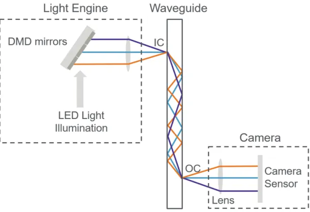
In augmented reality devices, waveguides with diffraction grating regions are used to propagate light from a light engine to the user. In order to transport the image, the waveguide must have an coupling and an out-coupling grating region. The in-coupling region (IC) allows the image to propagate into the waveguide. Conversely, image exits the waveguide at the out-coupler (OC), where it reaches the user’s eye.
Users have different interpupillary distances, face shapes, and nose heights. Con-sequently, given one waveguide device and multiple users, the location of a user’s pupil within the out-coupler region will change. Therefore, two-dimensional exit pupil ex-pansion is used to allow for light propagation to the user.
Conventionally, three grating regions are used for two-dimensional exit pupil ex-pansion. After light couples into the waveguide through the IC, the light propagates to a second grating region, the exit pupil expander (EPE). As light propagates through the EPE, light either diffracts and propagates towards the OC or continues propagat-ing within the EPE, allowpropagat-ing for exit pupil expansion in one direction. At the OC, the exit pupil is then expanded in the second direction. As light propagates through the OC, light either diffracts out of the waveguide to the pupil or continues propagating within the OC. [1] A diagram of a waveguide with three grating regions (IC, EPE, and OC) is shown in figure 1-1. Multiple eye positions are illustrated in the diagram. Given any eye position, the perceived image should be the same as the input image. In this example, the image is a seal icon. Given two-dimensional pupil expansion, a
user can perceive the full input image regardless of the eye position in relation with the OC.
Figure 1-1: Two-dimensional pupil expansion in a waveguide with three grating re-gions
.
The angular uniformity, spatial uniformity, resolution, field of view, and intensity of the image at the out-coupler are defined by input incident angle, grating parameters such as pitch (Λ), orientation (Γ), refractive index, duty cycle, and more. These parameters are optimized during the design process; however, manufacturing barriers limit the quality of the output image in a device.
The goal of the thesis is to build reliable measurement systems to qualify manu-factured waveguides and give insights on how to improve within the manufacturing process. The first system characterizes grating pitch and orientation. The second measures the resolution of the waveguide’s output image.
1.1
Motivation
1.1.1
Grating Characterization
High waveguide grating quality is essential for ensuring waveguide functionality, and two important parameters are pitch and grating orientation. The waveguides produced in-house have grating regions designed with uniform pitch and orientation. The pitch is the grating period and defines the distance between grating lines. Grating orientation is the rotation of the grating lines, relative to one of the grating lines. The waveguide samples characterized in this thesis are 1D line gratings. Therefore, within one grating region with uniform orientation, grating orientation should be 0∘, and the grating lines should be parallel. If grating orientation is not uniform, the grating lines will not be parallel. Pitch and orientation define the angle of light propagating within the waveguide, which affects display resolution. Therefore, grating manufacturing needs to be precise. with a uniform grating area, the current target is a pitch error less than 0.1𝑛𝑚 and an orientation error less than 0.15∘.
Accurate characterization of gratings can help internally to further develop the waveguide manufacturing process. By measuring waveguides at different steps in the manufacturing process, vulnerabilities within the process line can be identified. In addition, different design parameters can be harder to accurately manufacture, which can be identified with grating characterization.
1.1.2
Resolution
The resolution of the output image in a waveguide is defined by the resolution of the light engine and the ability of the waveguide to properly propagate the image from the light engine to the user. In this thesis, I will focus on the latter.
Measuring resolution qualifies the overall quality of the waveguide, and resolution is a specification for waveguide functionality given by customers. Therefore, build-ing a reliable system for waveguide resolution measurement will allow us to qualify manufactured waveguides and ensure that they meet specifications.
Another goal is to understand the correlation between grating uniformity and overall waveguide resolution. Since grating pitch and orientation define the angle of light propagation within the waveguide, a waveguide with poor grating pitch and orientation control is expected to have low waveguide resolution.
Given an input light ray and a waveguide with perfect grating pitch and orienta-tion, the ray will go through two-dimensional pupil expansion, and at the OC, the expanded rays will exit parallel to the input angle, illustrated in figure 1-1. Therefore, when injecting a full image into the IC containing rays with different input angles crossing a large field of view, the output image will consist of rays parallel to the input rays. In this scenario, the image will appear sharp.
However, if some of the input rays encounter a region where the grating pitch or orientation is not as designed, the light will then change its propagation angle, and consequently, when exiting the OC, the rays will no longer be parallel to the input rays. Therefore, the output ray angles will not map directly back to the input ray angles, and in this scenario, the image will appear blurry and smeared.
Understanding the correlation between grating uniformity and waveguide resolu-tion can help define grating uniformity tolerances necessary during manufacturing.
1.2
Prior Methods
Grating pitch and orientation can be measured with scatterometry. The overall device resolution can be defined by the modulation transfer function, MTF.
1.2.1
Grating Uniformity: Scatterometry
Given incident light of wavelength 𝜆 and grating pitch Λ, the incident ray will diffract when it hits a grating if 𝜆 ≤ 2Λ. By detecting the angle of two diffracted orders, such as 𝑚2 and 𝑚1, the pitch can be determined following equation 1.1.
Λ = (𝑚2− 𝑚1)𝜆 sin 𝜃2− sin 𝜃1
Given incident light at angle 𝜃𝑖, the 0𝑡ℎreflection order (R0) will reflect with angle
−𝜃𝑖. Furthermore, 𝜃𝑖 can be set so that the 𝑚𝑡ℎ’s diffraction angle, 𝜃𝑟, is reflected
parallel to 𝜃𝑖. This is defined as the Littrow configuration, where 𝜃𝑖 = 𝜃𝑟 = 𝜃𝐿, and
in this configuration, the pitch equation simplifies to equation 1.2.
Λ = 𝑚𝜆 sin 𝜃𝑖+ sin 𝜃𝑟 in Littrow = 𝑚𝜆 2 sin 𝜃𝐿 (1.2) Using this method, higher diffraction orders will increase precision of pitch grating measurements [2],[3]; however, higher diffraction orders are negatively affected by weak intensity, non-uniformity, and asymmetry in gratings [2]. Therefore, in the current application, the first reflection diffraction order (R1) is chosen.
Littrow Configuration Setup
A schematic for the Littrow configuration setup with R1 is shown in figure 1-2. A collimated light source and a CCD camera are mounted on one rotating arm set at the Littrow angle of the gratings to be measured.
Figure 1-2: Littrow setup for detecting R1 .
When the grating lines are set normal to the detecting arm and the rotating arm is set at the Littrow angle of the gratings, the CCD camera will display a beam spot at the center of the display. The collimated light source is not infinitesimally small, and the 488𝑛𝑚 laser used has a 2𝑚𝑚 by 2𝑚𝑚 aperture. Consequently, multiple grating
lines are covered by a single laser light spot, and the reflected light contains pitch and orientation information of all the gratings covered by the light spot. If the covered area is perfectly uniform, the rays will diffract with the same angle and the beam spot will be perfectly circular, illustrated in figure 1-3a. However, if there is variation within the measured gratings, the beam spot will appear ovular, illustrated in figure 1-3b. By analyzing the shape of the beam spot, pitch and grating orientation local variation across the 2𝑚𝑚 by 2𝑚𝑚 region can be extracted. Pitch and orientation uniformity of a larger grating area can be measured by implementing a motorized stage (in the Y-Z plane) which allows for measurements at different 2𝑚𝑚 by 2𝑚𝑚 spots in a larger grating area.
(a) Beam spot of uniform gratings (b) Beam spot of non-uniform gratings
Figure 1-3: Beam spot profiles of uniform and non-uniform gratings
During one set of measurements, the incident angle is set constant while the sample moves underneath the laser beam spot. At each measurement point, the R1 beam spot is captured by the CCD camera. The spatial movement of the beam spot in the camera translates to changes in the diffracted angle. If the pitch within the measured grating area changes, the system will no longer be in Littrow configuration. The R1 beam angle will change by ∆𝜃𝑅1, and the beam spot will move vertically in
the detector plane. If the grating orientation changes, the beam spot will change by ∆𝜑𝑅1, and the beam spot will move horizontally in the detector plane. By analyzing
uniformity can be measured. In addition, by examining the beam spot shape, the local variation of pitch and orientation at each measurement point can be measured. Given a ∆𝜃𝑅1 and ∆𝜑𝑅1 change in the diffracted beam angle, the pitch Λ and
orientation Γ can be calculated with equation 1.3 and equation 1.4.
Λ = 𝑚𝜆
sin 𝜃𝐿+ sin (𝜃𝐿+ ∆𝜃𝑅1)
(1.3)
Γ = ∆𝜑𝑅1
2 (1.4)
1.2.2
Resolution: Modulation Transfer Function
Modulation transfer function (MTF) characterizes the resolution and performance of an optical system by measuring the contrast of images produced after propagating through the optical system. The image contains information for a set field of view, determined by the camera’s focusing lens and sensor size, and therefore, the MTF for different input angles can be measured by analyzing different locations in the image. There are two main techniques to measure the MTF: line pair method and slant edge method.
Line Pair Method
A line pair image is a pattern with alternating black and white lines. An example of a line pair pattern with a spatial frequency defined with 3 pixels bright and 3 pixels dark is shown in figure 1-4.
For a fixed spatial frequency, the MTF describes the ability to resolve the linepairs, which is defined as the contrast between the bright and dark regions. The equation to calculate the MTF at a fixed spatial frequency is described in equation 1.5, where 𝐼 is an intensity value which ranges between pure dark and pure bright. During analysis, 0 is defined as pure dark and 1 is defined as pure bright.
𝑀 𝑇 𝐹 [𝑓 ] = 𝐼𝐿𝑖𝑛𝑒𝑃 𝑎𝑖𝑟𝑏𝑟𝑖𝑔ℎ𝑡− 𝐼𝐿𝑖𝑛𝑒𝑃 𝑎𝑖𝑟𝑑𝑎𝑟𝑘 𝐼𝐿𝑖𝑛𝑒𝑃 𝑎𝑖𝑟𝑏𝑟𝑖𝑔ℎ𝑡+ 𝐼𝐿𝑖𝑛𝑒𝑃 𝑎𝑖𝑟𝑑𝑎𝑟𝑘
Figure 1-4: Line pair test pattern .
Slant Edge Method
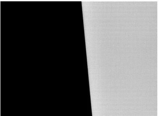
A slant edge is a pattern where a pure dark region is separated from a pure bright region by a slanted edge. An example of a slanted edge is shown in figure 1-5.
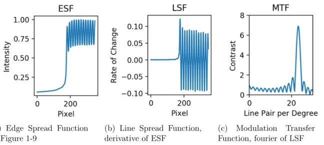
The MTF measures the sharpness of the transition between the bright and dark regions. The transition is defined as the edge spread function, ESF. To calculate the MTF, the derivative of the ESF, defined as the line spread function (LSF), is Fourier transformed. The calculated MTF is then normalized to 1 at 0 frequency.
𝐿𝑆𝐹 = 𝑑𝑖𝑓 𝑓 (𝐸𝑆𝐹 ) 𝑀 𝑇 𝐹 (𝑓 ) = ℱ (𝐿𝑆𝐹 ) 𝑀 𝑇 𝐹 (𝑓 ) = 𝑀 𝑇 𝐹 (𝑓 )
𝑀 𝑇 𝐹 (0)
Figure 1-5: Slant edge test pattern .
Current Setup
The current setup utilizes both the line pair and slant edge method to calculate the MTF.
A diagram of the system setup is illustrated in figure 1-6. In the system, the waveguide is positioned at the focal plane of the light engine, which is approximately 12𝑚𝑚 away from the light engine. The image is then injected into the waveguide’s IC and then propagated through the waveguide. The setup shown in figure 1-6 demon-strates ray propagation of three different input angles inside a waveguide with no exit pupil expansion. At the OC, a camera is placed to capture the image. The dis-tance between the camera and the OC is the eye-relief disdis-tance, and for this system, the eye-relief distance is set to approximately 15𝑚𝑚. The camera’s images are then analyzed to calculate the MTF of the waveguide.
The system’s light engine consists of a LED light source and a digital micro-mirror display, DMD, to create the line pair and slant edge images. There are three LEDs (red, green, and blue), and the current driving each LED can be independently
Figure 1-6: MTF setup and ray propagation with no exit pupil expansion
set. This allows for the system to measure the resolution of the optical system with different colors. The LEDs illuminate the DMD, which creates the test pattern. The DMD consists of microscopic mirrors arranged in a rectangular array, and the mirrors correspond to pixels in the projected image. Figure 1-7 shows a DMD composed of an array of micro-mirrors [4]. The mirrors can be individually rotated to either an "on" or "off" state, allowing for pattern creation. In addition, the DMD can also create gray-scale pixels by toggling the mirrors between its "on" and "off" states quickly, and the intensity of the projected pixel is proportional to the duty cycle of the "on" and "off" states of the mirrors. During the "on" state, a mirror is set to reflect the light out of the light engine, making the pixel appear bright. Conversely, during the off state, a mirror directs the light elsewhere, making the pixel appear dark. The resolution of the projected image is determined by the size and density of the rectangular mirror array, and resolution increases with higher mirror density.
Figure 1-7: Digital micro-mirror display [4]
1.3
Problems
1.3.1
Grating Uniformity: Sample Tilt
The diffracted beam angle is affected not only by non-uniformities in the grating pitch and orientation but also by system errors such as sample tilt. Sample tilt can be introduced by a non-balanced stage or by dust particles trapped between the sample and the stage. With the current Littrow configuration and analysis, the grating uniformity information cannot be decoupled from the sample tilt, and therefore, the true pitch and grating orientation uniformity cannot be extracted.
Samples with grating regions are created in-house on wafers, and multiple grating regions can be produced on one wafer sample. For example, the sample measured in figure 1-8 is a 8" wafer with 21 grating regions. The large wafers can be further diced in order to separate the individual grating regions into smaller samples to measure.
For small samples, the system error does not affect measurements significantly. However, with large samples, such as an 8" wafer, the sample tilt significantly affects the measurements. An example is shown in figure 1-8. In this example, the measure-ments display a strong gradient shift in both pitch and grating orientation uniformity. This gradient shift occurs from the sample tilt error, and the sample tilt dominates the underlying uniformity measurements. Therefore, no meaningful pitch or grating uniformity information can be extracted.
One goal of the thesis is to address the sample tilt error and to build a solution that enables grating pitch and orientation uniformity measurements for large sample sizes.
(a) Grating orientation uniformity (b) Pitch uniformity
Figure 1-8: Measured grating uniformity on a 8" wafer
1.3.2
Resolution: DMD Mirror Pixel Resolution
Using the line pair image method, MTF measurements are reliable and multiple field of view angles can be calculated with one image. However, the MTF calculated is only defined at the spatial frequencies projected, so multiple line pair images need to be captured. In addition, the MTF frequency measured is limited by the resolution of the system’s light engine and imaging camera. MTF at frequencies of up to 30 line pairs per degree (lppd) are desired. The current setup is limited by the light engine’s DMD mirror resolution, which allows for a maximum of 11.57 lppd.
On the other hand, the slant edge method produces a continuous MTF profile and allows for MTF measurements at higher frequencies. However, in the current system, the DMD mirrors used to create the test pattern has a significantly lower resolution than the camera sensor and a fill factor less than 1. Therefore, individual DMD mirror pixels are detected by the camera, and areas that should appear fully bright now appears pixilated. An example of the pixilated image is illustrated in
figure 1-9.
(a) Cropped slant edge image (b) Cropped and rotated slant edge image
Figure 1-9: Slant edge image showing pixilation from individual DMD mirrors
When analyzing such an image, the MTF will artificially spike at 22 lppd due to the frequency of the DMD pixels, shown in figure 1-10c. In addition to the peak at 22 lppd, there are also harmonics at lower and higher frequencies that affects the MTF signal. These harmonics dominate the underlying MTF information, and consequently, the slant edge method cannot work with the setup.
(a) Edge Spread Function of Figure 1-9
(b) Line Spread Function, derivative of ESF
(c) Modulation Transfer Function, fourier of LSF
Figure 1-10: MTF analysis on a pixilated slant edge image (figure 1-9)
The second goal of the thesis is to develop a reliable method to measure the MTF of a waveguide at high lppd using the current system with DMD mirror pattern
Chapter 2
Approach
In order to extract accurate grating uniformity information from the current setup, the sample tilt needs to be simultaneously measured. The first reflection diffraction order (R1) is affected by both the gratings and the sample tilt. On the other hand, the specular reflection, the zeroth order reflection (R0), is affected only by the tilt of the sample and not the gratings. From the specular reflection, the sample tilt can be measured, and therefore, grating uniformity can be calculated by decoupling the uniformity information from the sample tilt in the R1 measurements. This new method is further explained in section 2.1.
To measure a waveguide’s MTF at high lppd, a new method with single pixel illumination is proposed. By only illuminating one mirror in the DMD display, the pixilation problem from the slant edge is avoided. The MTF can then be measured from the profile of the illuminated pixel after propagation through the waveguide. This new method is further explained in section 2.2.
2.1
Grating Uniformity: R0 Detection
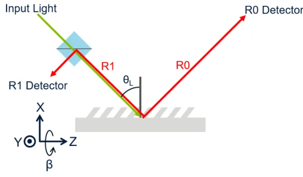
In order to detect the specular reflection, a second detector is added to the setup, shown in figure 2-1. The detector is placed on a rotating arm, which is set at the same but opposite angle as the input light.
Figure 2-1: Littrow setup for detecting R0 and R1 .
2.1.1
Angle and Coordinate System Definition
A front view of the Littrow setup with both R0 and R1 detectors is illustrated in figure 2-1. The stage is motorized to move along the X, Y, and Z axis. X-axis move-ment represents movemove-ment of the stage up and down, and during one measuremove-ment run, the stage’s X position stays constant. The stage’s X-axis is set so that the mea-sured beam spot is at the rotational center of both R0 and R1 arms, and therefore, the stage’s X-position changes for waveugides with different substrate thickness. During one set of measurements, the stage will only move in the Y-Z plane. Movement in the Z-axis represents movement towards the R0 or R1 detector, and movement in the Y-axis represents movement normal to the X and Z axis.
Due to system error, the sample can have an 𝛼 and 𝛽 rotation. 𝛼 rotation is defined as rotation around the Y-axis, either towards or away from the input light source, and a 𝛽 rotation is defined as rotation around the Z-axis. A balanced system with no sample rotation will have an 𝛼 and 𝛽 rotation of 0∘.
The reflected beam angle will be characterized by 𝜑 and 𝜃. 𝜑 is the angle of the reflected beam in the Y-Z plane around the X axis, with 𝜑 of 0∘ to be in-line with
the Z-axis. 𝜃 is the angle of the reflected beam in the X-Z plane around the Y axis, with 𝜃 of 0∘ to be normal to the sample and 𝜃 of 90∘ to be in-line with the sample.
2.1.2
Effect of Sample Tilt on R0
Because the specular reflection is not affected by the gratings, the system’s sample can be modeled as a mirror.
During one set of measurements, the input light is set to 𝜃𝐿, and the R0 detector is
set to −𝜃𝐿. Given no sample tilt, the beam focuses to the center of the detector, and
this pixel represents the reference R0 pixel. The reflected beam angle is characterized by 𝜃𝑅0= 𝜃𝐿 and 𝜑𝑅0 = 0∘, and this is the reference R0 beam angle.
An 𝛼 rotation will change the R0 reflection angle in the X-Z plane, and therefore, the beam spot will move vertically in the R0 detector plane, affecting the reflected 𝜃 beam angle by ∆𝜃𝑅0. Conversely, a 𝛽 rotation will change the R0 reflection angle in
the Y-Z plane, and the beam spot will move horizontally in the R0 detector plane, affecting the reflected 𝜑 beam angle by ∆𝜑𝑅0.
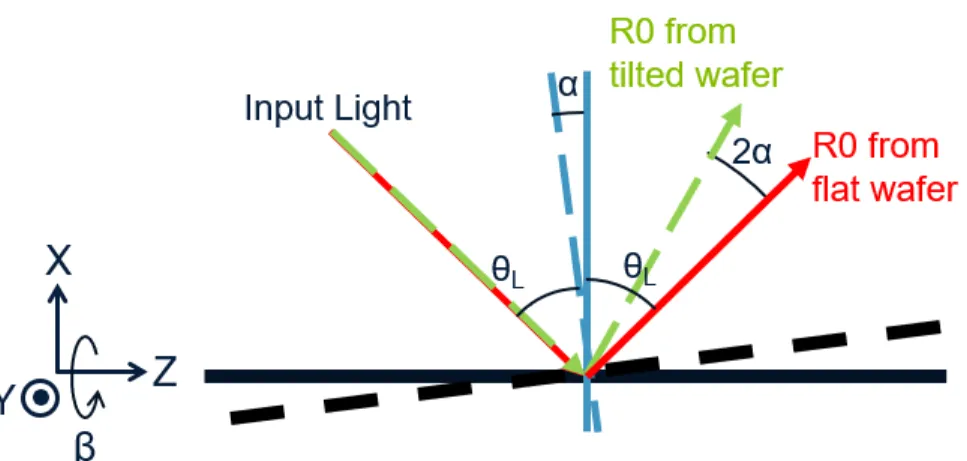
𝛼 Rotation
With an 𝛼 rotation, the incident angle with respect to the sample changes to 𝜃𝐿−𝛼.
The R0 beam will then reflect with angle 𝜃𝐿− 2𝛼, illustrated in figure 2-2. On the
CCD camera image, the R0 beam spot will focus to a different pixel corresponding to 2𝛼 degrees away the reference R0 pixel.
𝛽 Rotation
With 𝛽 rotation, the sample is tilted around the Z-axis, and the amount by which the reflected beam angle changes is dependent on both 𝛽 and the input angle 𝜃𝑖.
First, two extreme angles are examined, 𝜃𝑖 = 0∘ where the input angle is normal
to the sample, and 𝜃𝑖 = 90∘ where the input angle is in-line with the sample. When
𝜃𝑖 = 90∘, the reflected beam 𝜃𝑟 is constant regardless of the sample 𝛽 tilt, and
Figure 2-2: Effect of 𝛼 wafer tilt on the R0 diffraction angle .
these two extremes, it can be intuitively understood that the effect of 𝛽 rotation on the reflected angle decreases as 𝜃𝑖 increases.
The sample’s 𝛽 tilt is expected to be small, and therefore, with small-angle ap-proximation, the reflection matrix of a sample with a 𝛽 rotation and no 𝛼 rotation is defined as 𝑀𝑟 in equation 2.1. 𝑀𝑟 = ⎡ ⎢ ⎢ ⎢ ⎣ −1 + 𝛽2 −2𝛽 0 −2𝛽 1 − 𝛽2 0 0 0 1 ⎤ ⎥ ⎥ ⎥ ⎦ (2.1)
Given an input angle of 𝜃𝑖, the input light can be represented by vector 𝑘𝑖, shown
in equation 2.2. The resulting light vector after hitting the tilted mirror is 𝑘𝑜, shown
in equation 2.3. 𝑘𝑖 = ⎡ ⎢ ⎢ ⎢ ⎣ − cos 𝜃𝑖 0 sin 𝜃𝑖 ⎤ ⎥ ⎥ ⎥ ⎦ (2.2)
𝑘𝑜= 𝑀𝑟𝑘𝑖 = ⎡ ⎢ ⎢ ⎢ ⎣ −1 + 𝛽2 −2𝛽 0 −2𝛽 1 − 𝛽2 0 0 0 1 ⎤ ⎥ ⎥ ⎥ ⎦ ⎡ ⎢ ⎢ ⎢ ⎣ − cos 𝜃𝑖 0 sin 𝜃𝑖 ⎤ ⎥ ⎥ ⎥ ⎦ = ⎡ ⎢ ⎢ ⎢ ⎣ (1 − 𝛽2) cos 𝜃𝑖 2𝛽 cos 𝜃𝑖 sin 𝜃𝑖 ⎤ ⎥ ⎥ ⎥ ⎦ (2.3)
To determine the change in the reflected angle, 𝑘𝑜 needs to be compared to the
output vector given a system with 𝛽 = 0∘. 𝑘𝑜 is rotated by 𝜃𝑖 − 90∘, and therefore,
when 𝛽 = 0∘, the light only propagates in the Z-direction. The rotated output vector 𝑘𝑜′ is shown in equation 2.4. 𝑅𝑧′ refers to the rotation matrix of 𝜃𝑖 − 90∘ over the
Z-axis. 𝑘𝑜′ = 𝑅𝑧′𝑘𝑜 = ⎡ ⎢ ⎢ ⎢ ⎣ −𝛽2cos 𝜃 𝑖sin 𝜃𝑖 2𝛽 cos 𝜃𝑖 1 − 𝛽2cos2𝜃𝑖 ⎤ ⎥ ⎥ ⎥ ⎦ (2.4)
From 𝑘𝑜′, the reflected beam angle difference, ∆𝜑𝑅0 and ∆𝜃𝑅0 can be calculated.
∆𝜑𝑅0 is represented in equation 2.5, and ∆𝜃𝑅0 is represented in equation 2.6. ∆𝜃𝑅0
is very small and considered negligible.
∆𝜑𝑅0 = arctan 𝑘𝑜′ 𝑦 𝑘𝑜′ 𝑧 = 2𝛽 cos 𝜃𝑖 1 − 𝛽2cos2𝜃 𝑖 (2.5) ∆𝜃𝑅0 = arctan 𝑘𝑜′ 𝑥 𝑘𝑜′ 𝑧 = −𝛽 2cos 𝜃 𝑖sin 𝜃𝑖 1 − 𝛽2cos2𝜃 𝑖 (2.6)
2.1.3
Pitch Calculation
Given an input angle of 𝜃𝐿to a sample with no 𝛼 rotation, the R0 beam will reflect
with angle 𝜃𝐿back in the same direction. When the grating’s pitch deviates from the
ideal value, the diffraction angle equation changes by ∆𝜃𝑅1. Therefore, 𝜃𝑖 = 𝜃𝐿 and
𝜃𝑟 = 𝜃𝐿+ ∆𝜃𝑅1. An illustration of R1 diffraction given a sample with an 𝛼 rotation
is shown in figure 2-3.
When the sample is tilted by an 𝛼 rotation, the reference coordinate system with which to apply the diffraction angle equation changes, and the coordinate system also
Figure 2-3: Effect of 𝛼 wafer tilt on the R1 diffraction angle
tilts by 𝛼. Therefore, given the pitch equation shown in equation 1.2, 𝜃𝑖 = 𝜃𝐿− 𝛼,
and 𝜃𝑟 = 𝜃𝐿− ∆𝜃𝑅1− 𝛼, shown in equation 2.7.
𝜃𝑟′ + 𝛼 = ∆𝜃𝑅1+ 𝜃𝐿
𝜃𝑟′ = 𝜃𝐿− ∆𝜃𝑅1− 𝛼
(2.7)
Therefore, given the R0 and R1 beam angles, ∆𝜃𝑅0 and ∆𝜃𝑅1 are extracted, and
the grating’s pitch can be calculated by equation 2.8.
𝛼 = ∆𝜃𝑅0 2
Λ = 𝑚𝜆
sin (𝜃𝐿− 𝛼) + sin (𝜃𝐿− ∆𝜃𝑅1− 𝛼)
(2.8)
2.1.4
Grating Orientation Calculation
The model for the R1 reflected angle difference is similar to the one derived for the R0 reflected angle difference. However, in the Z-direction, the beam is reflected back towards the input light source, and therefore, the sign of the last matrix element which corresponds to the Z-direction in 𝑀𝑟 changes sign. The modified 𝑀𝑟 is shown
in equation 2.9. 𝑀𝑟 = ⎡ ⎢ ⎢ ⎢ ⎣ −1 + 𝛽2 −2𝛽 0 −2𝛽 1 − 𝛽2 0 0 0 −1 ⎤ ⎥ ⎥ ⎥ ⎦ (2.9)
signs as the relationship of ∆𝜑𝑅0 and ∆𝜃𝑅0 of the R0 beam. ∆𝜑𝑅1 and ∆𝜃𝑅1 are
defined in equations 2.10 and 2.11 respectively. Like ∆𝜃𝑅0, ∆𝜃𝑅1 from 𝛽 rotation is
small and considered negligible.
∆𝜑𝑅1,𝛽 = −2𝛽 cos 𝜃𝑖 1 − 𝛽2cos2𝜃 𝑖 (2.10) ∆𝜃𝑅1,𝛽 = 𝛽2cos 𝜃 𝑖sin 𝜃𝑖 1 − 𝛽2cos2𝜃 𝑖 (2.11) Grating orientation can be calculated by first isolating the ∆𝜑𝑅1 of the grating
orientation from the sample 𝛽 tilt, illustrated in equation 2.12. Grating orientation information can then be measured from the R1 phi angle beam change of the grating orientation, illustrated in equation 2.13.
∆𝜑𝑅1 = ∆𝜑𝑅1,𝑔𝑟𝑎𝑡𝑖𝑛𝑔 − ∆𝜑𝑅1,𝛽 ∆𝜑𝑅1 = ∆𝜑𝑅1,𝑔𝑟𝑎𝑡𝑖𝑛𝑔 + ∆𝜑𝑅0 (2.12) Γ = ∆𝜑𝑅1,𝑔𝑟𝑎𝑡𝑖𝑛𝑔 2 Γ = ∆𝜑𝑅1− ∆𝜑𝑅0 2 (2.13)
2.1.5
Local Variation Calculation
The local variation of a 2𝑚𝑚 by 2𝑚𝑚 region is measured by the shape of the R1 beam spot.
Given uniform pitch and orientation, the rays will all diffract with the same angle, creating a symmetric circle. The radius of the beam spot circle is determined by the width of the detecting laser’s beam.
With non-uniform pitch, the rays will no longer diffract at the same 𝜃 angle, and the beam spot can expand or contract vertically. With non-uniform orientation, the rays will not diffract with the same 𝜑 angle, and the beam spot will expand or contract horizontally.
maximum (FWQM) is compared with a reference width. The reference width refers to the FWQM of a beam given perfect uniformity within a 2𝑚𝑚 by 2𝑚𝑚 region, and the reference width for both 𝜑 and 𝜃 are the same. The widths are measured from the beam spot images, and the unit of widths are in pixels. The pixel values can be converted to angles using a constant, 𝐶. This constant has unit 𝑑𝑒𝑔𝑟𝑒𝑒𝑝𝑖𝑥𝑒𝑙 and is measured during calibration. Because the variation is measured using FWQM, it is essential for the beam spot to not oversaturate in the detector. If the beam spot is oversaturated, the variation calculated will be artificially high.
The orientation variation can be calculated by equation 2.14. The pitch variation can be calculated by equation 2.15. 𝜃𝑝𝑖𝑥𝑒𝑙,𝑟𝑒𝑓 corresponds to the reference pixel value
of the beam center when detecting a region with uniform pitch values. 𝜃𝑝𝑖𝑥𝑒𝑙,𝑙𝑒𝑓 𝑡 and
𝜃𝑝𝑖𝑥𝑒𝑙,𝑟𝑖𝑔ℎ𝑡 corresponds to the two pixel values where the measured beam spot reaches
25% of the beam maximum.
Γ𝑣𝑎𝑟𝑖𝑎𝑡𝑖𝑜𝑛 = 𝐶|𝐹 𝑊 𝑄𝑀𝑏𝑒𝑎𝑚− 𝐹 𝑊 𝑄𝑀𝑟𝑒𝑓| (2.14) 𝑎 = 𝐶[(𝜃𝑝𝑖𝑥𝑒𝑙,𝑟𝑒𝑓 − 𝐹 𝑊 𝑄𝑀𝑟𝑒𝑓 2 ) − 𝜃𝑝𝑖𝑥𝑒𝑙,𝑙𝑒𝑓 𝑡] 𝑏 = 𝐶[(𝜃𝑝𝑖𝑥𝑒𝑙,𝑟𝑒𝑓 − 𝐹 𝑊 𝑄𝑀𝑟𝑒𝑓 2 ) − 𝜃𝑝𝑖𝑥𝑒𝑙,𝑟𝑖𝑔ℎ𝑡] Λ𝑙𝑒𝑓 𝑡 = 𝑚𝜆 sin (𝜃𝐿− 𝛼) + sin (𝜃𝐿− 𝑎 − 𝛼) Λ𝑟𝑖𝑔ℎ𝑡 = 𝑚𝜆 sin (𝜃𝐿− 𝛼) + sin (𝜃𝐿− 𝑏 − 𝛼) Λ𝑣𝑎𝑟𝑖𝑎𝑡𝑖𝑜𝑛 = |Λ𝑙𝑒𝑓 𝑡− Λ𝑟𝑖𝑔ℎ𝑡| (2.15)
2.2
Resolution: Single Pixel Illumination
The optical transfer function (OTF) can be described as the Fourier transform of a point spread function, PSF [5]. The OTF is a complex-valued function, shown in equation 2.16. By definition, the modulation transfer function (MTF) is defined as the absolute value of the OTF, and the phase transfer function (PhTF) is defined as the complex argument of the OTF.
𝑂𝑇 𝐹 = 𝑀 𝑇 𝐹 𝑒𝑖𝑃 ℎ𝑇 𝐹 𝑀 𝑇 𝐹 = |𝑂𝑇 𝐹 | 𝑃 ℎ𝑇 𝐹 = 𝑎𝑟𝑔(𝑂𝑇 𝐹 )
(2.16)
When using single pixel illumination, only one DMD pixel is illuminated in a pattern. This single DMD pixel is first propagated through the light engine, where the pixel is convoluted with the light engine’s PSF. Then, the image propagates through the waveguide, where it is convoluted with the waveguide’s PSF to produce the output beam spot detected by the camera. The relationship between the input DMD pixel and the output beam spot is described in equation 2.17, where 𝑏𝑊 is
the waveguide’s output beam spot, 𝑝 is the DMD pixel, 𝑃 𝑆𝐹𝐿𝐸 is the point spread
function of the light engine, and 𝑃 𝑆𝐹𝑊 is the point spread function of the waveguide.
𝑏𝑊 = (𝑝 * 𝑃 𝑆𝐹𝐿𝐸) * 𝑃 𝑆𝐹𝑊 (2.17)
The Fourier transform of the waveguide’s PSF defines the waveguide’s OTF, and therefore, the MTF can be calculated by equation 2.18.
ℱ (𝑏𝑊) = ℱ (𝑝)ℱ (𝑃 𝑆𝐹𝐿𝐸)ℱ (𝑃 𝑆𝐹𝑊) 𝑀 𝑇 𝐹 = |ℱ (𝑃 𝑆𝐹𝑊)| = | ℱ (𝑏𝑊) ℱ (𝑝)ℱ (𝑃 𝑆𝐹𝐿𝐸) | (2.18)
The beam spot image captured by illuminating the camera directly from the light engine, 𝑏𝐿𝐸, describes the DMD pixel convoluted by the light engine’s PSF, 𝑝*𝑃 𝑆𝐹𝐿𝐸.
The beam spot image captured after the waveguide describe the final beam spot output, 𝑏𝑊. Therefore, the MTF can be calculated by comparing the light engine’s
and the waveguide’s beam spot, shown in equation 2.19.
𝑀 𝑇 𝐹 = |ℱ (𝑏𝑊) ℱ (𝑏𝐿𝐸)
2.3
Experimental Results
2.3.1
Grating Uniformity
Like the original scatterometry setup, the setup uses a 488𝑛𝑚 wavelength laser with a 2mm aperture as the input light. The modified scatterometry setup includes two CCD cameras, one to detect the R0 beam spot and another to detect the R1 beam spot. Due to limitations in the mounting configurations, the two cameras are mounted 90∘ from each other, and therefore, the 𝜑 and 𝜃 directions are different for the R0 and R1 beam images.
For the R0 beam images, ∆𝜃𝑅0, which results in vertical movement in the detector
plane, causes the beam spot to move up and down in the image. Conversely, ∆𝜑𝑅0,
which results in horizontal movement in the detector plane, causes the beam spot to move right and left in the image. For R1 beam images, ∆𝜃𝑅1, which results in
vertical movement in the detector plane, causes the beam spot to move right and left in the image. Conversely, ∆𝜑𝑅1, which results in horizontal movement in the detector
plane, causes the beam spot to move up and down in the image.
An example of a R0 and R1 beam spot taken from the modified scatterometry setup is illustrated in figure 2-4.
(a) R0 beam spot (b) R1 beam spot
2.3.2
Resolution
The single pixel illumination method requires illuminated single pixel images from the output of the waveguide and the output of the light engine. Like line pair analysis, the MTF at multiple field of view angles can be calculated with one image capture if there are single pixel illuminated beam spots at different regions of the image. To maximize the amount of beam spots that can be analyzed, a grid of single pixels are illuminated, spaced far enough apart so that each pixel is isolated.
The system setup for images from the output of the waveguide is displayed in figure 1-6. The system setup for images directly from the output of the light engine is displayed in figure 2-5
Figure 2-5: MTF system setup for obtaining light engine beam spot output
An example of illuminated beam spot images from the light engine and waveguide is illustrated in figure 2-6. Figure 2-6a describes 𝑏𝐿𝐸, and figure 2-6b describes 𝑏𝑊.
As expected, the beam spots from the light engine are smaller than the beam spots from the waveguide. The wider the beam spots in the waveguide images, the lower the expected MTF.
(a) Light engine: grid of illuminated green single pixel beam spots
(b) Waveguide 1: grid of illuminated green single pixel beam spots
Chapter 3
Analysis
3.1
Grating Uniformity
3.1.1
Image Analysis on Experimental Results
During analysis, one set of R0 and R1 images is used as the reference. For most measurements, the R0 and R1 images taken at the center of the grating area are used as the reference images. The R0 center and R1 center pixels are used as the reference pixels and angles for analysis.
The other beam spot center pixels are compared to the reference. When mounting the cameras, the image pixels per degree was calibrated and measured. The R0 image has 1439𝑑𝑒𝑔𝑟𝑒𝑒𝑝𝑖𝑥𝑒𝑙 , and the R1 image has 1768𝑑𝑒𝑔𝑟𝑒𝑒𝑝𝑖𝑥𝑒𝑙 . By comparing the center pixel values of the current set of image to the reference image, ∆𝜃𝑅0, ∆𝜑𝑅0, ∆𝜃𝑅1, and ∆𝜑𝑅0 can
be obtained.
The local grating orientation can be calculated with equation 2.13, and the local pitch can be calculated with equation 2.8. In addition, the local variation of pitch and orientation is calculated with equation 2.15 and 2.14. The R1 detector is more sensitive to ambient light and noise at the bottom of the detector, and therefore, the raw background intensity increases at the bottom of the detector. This increase in background intensity with the presence of a beam spot is shown in figure 3-1a. With this beam spot profile, the measured FWQM is artificially high at 1875 pixels. In
order to accurately measure the FWQM of the beam spot, the underlying background intensity has to be removed. The beam spot profile after the background intensity is removed is shown in figure 3-1b, and with the removed background intensity, the measured FWQM is more reasonable at 155 pixels.
(a) Rising background intensity: FWQM = 1875 pixels
(b) Removed background intensity: FWQM = 155 pixels
Figure 3-1: Effect of removing background intensity on FWQM for local variation calculation
Uniformity and variation analysis is performed, and the analysis code produces a text file that includes the pitch and orientation mean and local variation for every beam spot measurement. An short snippet of an example text file produced is shown in appendix A.3 and A.4. The information within the text file can be used to create a two dimensional measurement map in order to easily visualize and synthesize the data. Examples of measurement maps to visualize the grating pitch and orientation uniformity is shown in figure 3-3.
3.1.2
Results
Given grating samples on a 8" wafer, analyzing only the R1 beam spot yields results with a strong gradient shift of pitch in the Z-direction and grating orientation in the Y-direction, shown in figure 1-8.
By detecting the R0 beam spot, information of the underlying sample tilt can be measured. The 𝛼 and 𝛽 tilt of the sample is illustrated in figure 3-2. There is a
gradient 𝛼 tilt in the Z-direction, which corresponds to the gradient pitch measure-ments taken from only the R1 beam spot. Similarly, there is a gradient 𝛽 tilt in the Y-direction, which corresponds to the gradient orientation measurements taken from only the R1 beam spot.
(a) Alpha tilt (b) Beta tilt
Figure 3-2: Measured 𝛼 and 𝛽 sample tilt from R0
With the new analysis, the sample 𝛼 and 𝛽 tilt is accounted for, and the grating uniformity measurements no longer display any gradient shift. The new uniformity measurements are displayed in figure 3-3.
(a) Grating orientation uniformity (b) Pitch uniformity
The grating local variation for these measurements are shown in figure 3-4. The local variation measurements taken from only the R1 beam spot show no gradient shift, and those taken with the new analysis also show no gradient shift.
(a) Local orientation variation (b) Local pitch variation
Figure 3-4: Measured grating local variation variation from R0 and R1 beam spots
3.1.3
Simulation Validation
To validate the new analysis, a model of the two camera scatterometer system was created in LightTrans. The model, as setup in LightTrans, is composed of four subsystems: the input light path, the sample which the light reflects from, the R1 detection path, and the R0 detection path. The model, as created in LightTrans, is shown in figure 3-5. The distances between these subsystems are shorter than that of the physical system in order to speed up simulation.
Setup
The sample used is a waveguide with gratings. The grating period and orientation can be specified during simulation. The waveguide substrate is 0.6𝑚𝑚 thick with a 1.8 refractive index. Ideal gratings are used so there is only front side reflection from the gratings, with 50% light directed to R0 and 50% light directed to R1. With ideal gratings, backside reflection and higher diffraction orders are suppressed.
Figure 3-5: LightTrans system path
The input light path includes a 488𝑛𝑚 gaussian wave light source with a 2𝑚𝑚 by 2𝑚𝑚 diameter. The R1 detection path includes a detector of size 20𝑚𝑚 by 20𝑚𝑚 placed 80𝑚𝑚 away from the sample. The detector has a resolution of dictated by 81922 sampling points. Both the input light path and the R1 detection path are set at the Littrow angle of the sample gratings.
The R0 detection path includes a detector placed 80𝑚𝑚 away from the sample. Like the R1 detector, this detector is 20𝑚𝑚 by 20𝑚𝑚 and has a resolution dictated by 81922 sampling points. The R0 detection path is placed at the opposite but equal angle of the R1 detection path and the input light.
An example of a system with grating period 380𝑛𝑚 and Littrow angle 39.95∘ is shown in figure 3-6. An example of the R1 detector output is shown in figure 3-7. With no wafer tilt and the detectors placed at the Littrow angle, the beam spot location should be at the center of both detectors.
Simulation and Analysis
To mimic the wafer tilt, the sample’s 𝛼 and 𝛽 angles are changed independent of positions and angles of the other subsystems. To mimic grating non-uniformities, the pitch and grating orientation are altered independently without affecting the original angles of the other subsystems. For example, given an ideal grating period of 488𝑛𝑚
Figure 3-6: LightTrans system path for a grating sample with a 380 nm pitch
and grating orientation of 0∘, the subsystems are set at the Littrow angle, 30∘. The grating period is then swept ±0.2𝑛𝑚, the grating orientation is swept from 0∘ to 0.05∘, and 𝛼 and 𝛽 angles are swept from 0∘ to 0.1∘.
Grating orientation cannot be set explicitly on LightTrans. Instead, the angled direction with which the grating orders get directed to can be set. However, this angle is not equal to the orientation of the pitch, and the orientation of the pitch is equal to half of the set grating order output orientation. For example, a grating order output of 30∘ represents grating orientation of 15∘.
Within LightTrans, the beam spot image centers can be obtained. These image centers can then be analyzed similar to that in the physical scatterometer setup.
Results
The results from a 𝛼, 𝛽, pitch, and grating orientation parameter run with an ideal pitch of 380 nm and orientation of 0∘ is attached in appendix A.1.
The analysis produces grating measurements attached in appendix A.2. With the analysis, the 𝛼 and 𝛽 angles calculated has a maximum error of 0.004564∘. The calculated grating orientation, Γ, has a maximum error of 0.009408∘, and the pitch, Λ, has a maximum error of 0.068𝑛𝑚. These errors are within the allowed system’s margin of error.
3.2
Resolution: MTF
3.2.1
Image Analysis on Experimental Results
During analysis, the beam spot grid images from the light engine and waveguide images are analyzed. From the images, individual beam spots are cropped. The horizontal MTF is calculated by analyzing the horizontal cross section of the beam spot, and the vertical MTF is calculated by analyzing the vertical cross section of the beam spot.
waveg-uide’s resolution at different input angles to be measured. The images taken have a total field of view of 8∘ vertically and 13∘ horizontally. During analysis, the grids of beam spots are separated into nine sections, which each section representing a differ-ent input angle. For example, given a system setup with normal incidence, the nine sections will correspond to a horizontal input angle of −3.25∘, 0∘, and 3.25∘ and a vertical input angle of −2∘, 0∘, and 2∘.
In order to reduce mirror to mirror variation and system noise, multiple beam spots which fits a specified intensity criteria within each of the nine beam spot image sections are averaged. The beam spot intensity criteria and beam spot averaging are further discussed below.
After averaging, a Fourier transform is applied to both the horizontal and vertical beam spot cross section. Given the limited resolution of the imaging system, the beam spot images must first be zero-padded to obtain higher resolution in the frequency domain after Fourier transformation. After performing the Fourier transformation to both the light engine and the waveguide beam spots, a complex division between the waveguide and the light engine is performed, which yields the OTF. The MTF is then calculated by taking the magnitude of the OTF.
Beam spots are not symmetrical, and an extreme example is shown in figure 3-8. The horizontal MTF is defined by both the profile of the beam fading from the center to the left and from the center to the right. In this example, the beam fades slower to the left than to the right, and therefore the horizontal MTF from the center to the left (𝑀 𝑇 𝐹𝑙𝑒𝑓 𝑡) will be lower than the horizontal MTF from the center to the right
(𝑀 𝑇 𝐹𝑟𝑖𝑔ℎ𝑡). To account for this, the final horizontal MTF is the average of 𝑀 𝑇 𝐹𝑙𝑒𝑓 𝑡
and 𝑀 𝑇 𝐹𝑟𝑖𝑔ℎ𝑡. Similarly, for vertical MTF, the vertical MTF from the center to the
top and the vertical MTF from the center to the bottom are averaged.
When computing the analysis using Python, the output is a list of MTF values, and the line pair per degree with which each of the MTF value corresponds to is defined by both the individual beam crop size and the zero-padding factor. Given a crop size of 𝑠 and a zero-padding factor of 𝑧, the length of the output MTF value list is 𝑠 * 𝑧. The list of line pairs per degree with which the MTF values correspond to is
Figure 3-8: Non-symmetrical waveguide beam Spot
calculated in equation 3.1. A horizontal cross section of the camera’s output image contains 4028 pixels and spans 13∘, and therefore, the constant defining 𝑑𝑒𝑔𝑟𝑒𝑒𝑝𝑖𝑥𝑒𝑙𝑠 is 402813 .
𝑙𝑝𝑝𝑑 = [1, 2, 3, ..., 𝑠 * 𝑧] 𝑠 * 𝑧 * 4028 13 [ 𝑝𝑖𝑥𝑒𝑙𝑠 𝑑𝑒𝑔𝑟𝑒𝑒] * 1 2[ 𝑙𝑖𝑛𝑒 𝑝𝑎𝑖𝑟𝑠 𝑝𝑖𝑥𝑒𝑙 ] (3.1)
Beam Spot Intensity Criteria
The intensity of the individual beam spots, after propagating through the waveg-uide, is dependent on the waveguide’s efficiency. A waveguide with low angular uni-formity can lead to a beam spot image grid with varying beam spot intensities.
Beam spot oversaturation in the camera will lead to a cutoff in the beam spot profile, which affects the Fourier transform. Conversely, if the efficiency of the beam spot is too low, a higher portion of the beam spot profile will be cutoff by the camera sensor’s threshold. Consequently, the amount of pixels containing beam spot infor-mation decreases, and there will not be enough inforinfor-mation for a reliable Fourier transformation.
Therefore, during analysis, oversaturated and extremely undersaturated beam spots need to be ignored, and only beam spots with maximum intensities between
100 256 and
255
256 are analyzed. Given one image, there can be some angles with no beam
spots which fit the beam spot intensity criterion. In these cases, the MTF for some angles cannot be calculated.
Beam Spot Averaging
Performing a Fourier transform on a beam spot is highly sensitive towards noise or fluctuations in the system. These fluctuations occur from noise spikes in the CCD camera, DMD mirrors, and the refresh rate of the imaging system. To suppress variations and increase reliability, beam spot images are averaged over 10 captures. Figure 3-9 illustrates the affect of averaging over 10 captures. The graph on the left is a cross section of three beam spots with only 1 capture per image while the graph on the right is a cross section of three beam spots from an average of 10 captures. The graph on the right shows a smooth intensity profile while the graph on the left shows a more ragged intensity profile which comes from fluctuations in the system.
Figure 3-9: Comparing beam spots from one capture and from the average of ten captures
In addition, to further reduce mirror to mirror variation and system noise, multiple beam spots are averaged together.
3.2.2
System Setup
In order to achieve maximum beam spot output intensities between 100256 to 255256, several system parameters can be tuned: the LED current, camera sensor gain, and the duty cycle of the DMD mirrors.
Camera Gain
Changing the camera’s gain controls the amplification of the signal from the cam-era sensor, and the gain of the system can be set from 0 to 100. Gain amplifies the whole signal, including the associated background noise.
An experiment was run to see the reliability of changing the gain in a system. Given one wafer and a single beam spot location, the beam spot was captured at different gains with a DMD duty cycle of 100% and a current of 200 mA. The raw profile of the horizontal cross-section of the beam spot is shown in figure 3-10a. Ideally, once normalized, the beam profiles will be identical, thus producing the same MTF. However, the normalized profile of the horizontal cross-section shows that the higher the gain, the wider the normalized beam spot, illustrated in figure 3-10b. The gain effect on the signal is non-linear, and the gain more significantly affects lower intensities. The change in beam spot profiles will lead the measured MTF to decrease as the gain increases. Since the same beam spot is being measured across the different gains, the change in MTF is artificial. Therefore, across all measurements, the same gain factor must be used.
(a) Raw profile (b) Normalized profile
LED Current
Changing the current of the LEDs changes the intensity of the incoming light signal, and the currents of the system’s LEDs can be tuned from 0 to 500 mA.
An experiment was run to see the reliability of changing the current in a system. Figure 3-11 shows an individual light engine beam spot at two different currents: 200 mA and 500 mA. High currents, such as the one in figure 3-11b lead to ghosting of the pixel. The ghosting effect occurs with varying degrees for different LED currents and color. For blue and green, the ghosting becomes visibly noticeable at currents > 300 mA, and for red, the ghosting becomes visibly noticeable at currents > 500 mA.
‘
(a) Current 200 (b) Current 500
Figure 3-11: Beam spots at different LED currents
For the proposed single pixel analysis, the light engine beam spot images are assumed to be the input to the waveguide. If the currents for the light engine and waveguide beam spot images are different, then the light engine image is no longer the input to our waveguide. Therefore, the current across the light engine and waveguide measurements must be constant. In order to reduce variability, the current across all measurements, even with different waveguides, are set to be constant for each color.
trans-form of the beam spot decays faster. If the light engine FFT reaches 0, then the MTF, defined as the waveguide’s FFT divided by the light engine’s FFT, will approach infin-ity. Therefore, having a high Fourier transform for the light engine is ideal. Therefore, not only should the current be constant across all measurements, the ghosting effect should also be minimized, which is achieved by using lower current values.
Final System Parameters
The camera’s gain and LED current of the system must be set constant across all measurements in order to fairly compare the MTF across different waveguides. Because of the inefficiency of waveguides, high currents and gains are preferred. How-ever, current needs to be set low to avoid beam spot ghosting. Therefore, for green and blue, the LEDs are set to 200 mA, and for red, the LED is set to 500 mA. The red LED is much weaker than the blue and green LEDs, and therefore, the red LED needs to be driven by a higher current. With these current values, the gain needs to be set high so that the intensity of the output beam spots are in a valid range. At gains > 25, the amplification of the background noise becomes significant, causing "haze" in the background. This haze affects the calculated MTF. Therefore, the gain is set safely below 25 at 20.
However, in efficient waveguides, these parameters will cause the beam spots to oversaturate. Two methods are used to address oversaturation. The first technique is to add neutral density filters to the optical light path, and the second technique is to lower the duty cycle of the DMD mirrors. Adding filters lower the overall beam spots intensities across a whole image. However, to further tune the intensities, the duty cycle of DMD mirrors can also be changed. By lowering the duty cycle, the beam spot intensity will also lower. The duty cycle of individual mirrors can be tuned. This helps with angular non-uniformity, allowing for more beam spots in the beam spot grid to be analyzed.
3.2.3
Results
Single Waveguide Result
The averaged vertical beam spot cross sections at different input angles for a light engine and waveguide sample are shown in figure 3-12.
‘
(a) Light Engine (b) Waveguide
Figure 3-12: Light engine’s and waveguide’s vertical beam spot profile
The vertical MTFs of a waveguide sample at different input angles, given the beam spot cross sections shown in figure 3-12, are illustrated in figure 3-13. For several angles, the MTF at higher lppd artificially rises. One extreme example occurs with input angle (−3.25∘, 2∘), and the MTF rises after 25 lppd. This occurs because of the low light engine Fourier transform values at high lppd. This phenomena limits the range of lppd with reliable MTF measurements, and with the current results, the range for reliable MTF measurements is 0 to 20 lppd.
The averaged MTF across all FOV angles calculated using the single pixel illu-mination method is compared to the averaged MTF calcualted using the line pair method. A table with the MTF values at lppd 11.57, 5.78, and 3.86 are shown in table 3.1. With this example, the maximum error between the two methods is < 5%, which occurs at 11.57 lppd.
na
Figure 3-13: Light engine and waveguide Fourier transform and corresponding MTF for beam spot profiles in figure 3-12
lppd Single Pixel Illumination MTF Line Pair MTF
3.86 0.924393 0.926581
5.78 0.853135 0.835765
11.57 0.631428 0.66241
Waveguide Comparisons
When using the set system parameters, MTF results from different waveguides can be fairly compared, and the MTF of four different sample waveguides illuminated with green beam spots are compared in figure 3-15. To easily compare MTF efficiencies across different waveguides, the MTF curves for multiple input angles are averaged.
Examples of an individual beam spot in the beam spot grid array for each of the four samples are shown in figure 3-14b, 3-14c, 3-14d, and 3-14e. An example of the light engine beam spot is shown in figure 3-14a. Given the full beam spot grid, the analysis produces MTF results shown in 3-15.
Sample 3 shows the biggest beam spot, indicating that this waveguide’s point spread function is the widest. Therefore, the MTF of this sample is the lowest, demonstrated in the green in figure 3-15. In addition, all sample beam spots showcase an ovular shape, with the beam spot longer in the vertical than in the horizontal direction. Therefore, the vertical MTF is consistently worse than the horizontal MTF. In figure 3-15, the vertical MTF is represented as dashed lines while the horizontal MTF is represented as solid lines, and the dashed lines are consistently lower than the solid ones.
‘
(a) Light Engine
(b) Sample 1 (c) Sample 2
(d) Sample 3 (e) Sample 4
Chapter 4
Discussion
In this chapter, the limitations of the two new analysis methods for grating uni-formity and waveguide resolution measurements will be discussed. Further work to extend the application and reliability of both analysis methods will be explored.
4.1
Grating Uniformity
4.1.1
Limitations
Camera Alignment Sensitivity
The analysis requires the ability to decouple horizontal and vertical beam move-ment. In the current analysis, the horizontal and vertical beam movement, which we can define as the X’-Y’ coordinate system, is assumed to be aligned with the CCD camera’s X-Y coordinate system, and therefore, accurate CCD camera rotational alignment is crucial.
The CCD camera rotational alignment is set during system calibration. During calibration, a grating sample is placed on the stage, and both R0 and R1 CCD camera arms are set to 𝜃𝐿 (the input angle will also be set at 𝜃𝐿). The input angle will then
be stepped from 𝜃𝐿− 2∘ to 𝜃𝐿+ 2∘. While stepping through the angles, the R0 and
R1 rotational alignments are continuously adjusted until the beam spot only moves along one axis during input angle rotation. In the R1 CCD image, the beam spot
should move horizontally, and in the R0 CCD image, the beam spot should move vertically.
However, between calibrations, the camera’s rotational alignment will drift. There-fore, the beam movement’s X’-Y’ coordinate system will drift away from the image’s X-Y coordinate system. Consequently, the ability to decouple the horizontal and vertical beam spot movement also decreases, degrading the measurement’s reliability. This problem can be addressed by taking one additional set of beam spot images. At the beginning of each measurement run, an additional R0 and R1 image where the input light source is rotated slightly off of 𝜃𝐿, such as 𝜃𝐿+ 0.5∘, should be captured.
It is essential that the stage’s Z-position is set so that the sample gratings are placed at the center of the rotating arms. Therefore, the beam spot area being measured at the two input angles, 𝜃𝐿 and 𝜃𝐿+ 0.5∘, are identical. Afterwards, the input angle
must be set back to 𝜃𝐿 before continuing with the measurement run. By comparing
the beam spot positions of one grating area at input angle 𝜃𝐿 and 𝜃𝐿+ 0.5∘ will allow
the analysis to properly define the X’-Y’ coordinate system to decouple horizontal and vertical beam movement. Therefore, the measurements can still be reliable even after the CCD camera’s rotational alignment drift.
Beam Spot Interference Bands
There are multiple ray paths for the R0 and R1 diffraction orders. The first is reflection from the top side of the grating sample. The second is reflection from the bottom of the sample. When first interacting with the top side of the grating sample, some light continues to transmit through the grating and is then internally reflected within the substrate. Once these light rays hit the gratings, the rays will diffract back to the R0 or R1 camera. Ray paths demonstrating reflection from the top and bottom of the grating sample is shown in figure 4-1.
The differences between the light paths are given by the refractive index and thickness of the waveguide substrate, and with some waveguide samples, interference can occur resulting in constructive or destructive interference bands in the R0 and R1 beam spot. Figure 4-2 illustrates two examples of R0 beam spot with destructive
(a) R0
(b) R1
Figure 4-1: Ray paths for R0 and R1 with front-side and back-side reflection
interference. Interference bands changes the beam spot profile and analyzed beam spot center, which negatively affects the measurements.
(a) Example 1 (b) Example 2
Figure 4-2: R0 beam interference examples
Two techniques can be applied to address the interference bands within the beam spot. The first technique is to increase the exposure of the camera, allowing for the image to oversaturate. The second is to post-process the beam spots with blurring and dilation. By reducing the affect of interference bands, these two techniques help with accurate beam spot center detection.
For the R0 beam spot, only the center of the beam spot is needed for analysis. Therefore, these two techniques can be applied to the R0 beam spots.
analysis. The first technique of over-saturating changes the beam spot profile; the FWQM increases, causing the local variation to also artificially increase. Similarly, the second technique of blurring and dilation will also change the beam spot profile and increase the beam profile’s FWQM. Therefore, the two techniques cannot be applied to the R1 beam spot. Further methods need to be explored to reduce the affect of beam spot interference bands while still allowing for local variation measurements.
4.1.2
Further Work
Analyzing Beam Spot Intensity
In the R1 CCD camera, the beam spot intensity represents the local R1 efficiency. R1 efficiency is affected by grating parameters such as pitch, fin height, and duty cycle.
When measuring a grating sample area with uniform pitch and given constant camera settings such as exposure and gain, locations where beam spot intensity sig-nificantly increases or decreases indicates boundaries where grating parameters such as fin height or duty cycle changes.
4.2
Resolution
4.2.1
Limitations
Low Efficiency Waveguides
The camera’s gain and LED currents are set constant across all measurements. Given a waveguide with high efficiency, the duty cycle of the DMD mirrors can be changed to lower the output beam spot intensity. However, given a waveguide with low efficiency, the gains and LED currents cannot be increased to raise the output beam spot intensity. Therefore, the MTF of low efficiency waveguides cannot be measured.


![Figure 1-7: Digital micro-mirror display [4]](https://thumb-eu.123doks.com/thumbv2/123doknet/13828380.443070/21.918.135.705.114.327/figure-digital-micro-mirror-display.webp)