HAL Id: hal-01497515
https://hal.archives-ouvertes.fr/hal-01497515
Submitted on 29 Mar 2017
HAL is a multi-disciplinary open access
archive for the deposit and dissemination of
sci-entific research documents, whether they are
pub-lished or not. The documents may come from
teaching and research institutions in France or
abroad, or from public or private research centers.
L’archive ouverte pluridisciplinaire HAL, est
destinée au dépôt et à la diffusion de documents
scientifiques de niveau recherche, publiés ou non,
émanant des établissements d’enseignement et de
recherche français ou étrangers, des laboratoires
publics ou privés.
Impact of non-linear capacitances on transient
waveforms during system level ESD stress
Fabien Escudié, Fabrice Caignet, Nicolas Nolhier, Marise Bafleur
To cite this version:
Fabien Escudié, Fabrice Caignet, Nicolas Nolhier, Marise Bafleur. Impact of non-linear capacitances
on transient waveforms during system level ESD stress. Microelectronics Reliability, Elsevier, 2016,
Proceedings of the 27th European Symposium on Reliability of Electron Devices, Failure Physics and
Analysis, 64, pp.88 - 92. �10.1016/j.microrel.2016.07.046�. �hal-01497515�
Impact of Non-linear Capacitances on Transient Waveforms during
System Level ESD stress
F. Escudié, F. Caignet, N. Nolhier
a, M. Bafleur
LAAS-CNRS, Université de Toulouse, CNRS, UPS, Toulouse, France
Abstract
Prediction of failures induced during system level ESD stress is mainly related to the transient waveforms at chip level. To investigate hard and soft failures a precise modeling of the system is required. On-chip protection models can be obtained using quasi-static measurements. Even if such models can achieve good ESD simulations the impact of the external elements are more important. Paper deals with non-linear behaviors of the external elements related to the on-chip protections. Characterization techniques and models are presented, based on two types of capacitances, two different values, placed in parallel to on-chip protections. The paper shows the important variations of X7R capacitances during stresses that change the waveforms at the input of the chip. In measurements different behaviors are observed and reproduced by simulation. The methodology to build model and simulation will be presented.
1. Introduction
Achieving system level electrostatic discharge (ESD) reliability is a main challenge in embedded systems regarding ElectroStatic Discharges (ESD). The analysis and understanding of malfunction is usually very difficult because all the elements will impact the stress propagation into the Integrated Circuits (IC). At die level two types of failures can be distinguished. One causing permanent damages, such as the destruction of the electronic system, called “Hard failure”. The second called “Soft or Functional failure” leads to temporary loss of function. In both cases it is particularly important to prevent failures and it is more crucial for applications that require very high level of safety. To predict the impact of such transient events, System Efficient ESD Design (SEED) approach is required [1]. Several studies were carried out to predict the impact of ESD at system level based on models created by I(V) curves generated by Transmission Line Pulse (TLP) testing [2,3,4,5,6,7]. In these studies quasi-static simulations are performed to predict hard failures. However, the prediction of soft failures require precise dynamic simulations . In this paper, we focus on transient simulation and on the impact of modeling of external elements like capacitors largely used to absorb transient events. We will show that the non-linear behavior of X7R type capacitors can largely differ during stresses and then impact the IC responses. In this study we used different providers of a LIN (Local Interconnect Network) device, which allows different behaviors of on-chip protections [9]. Capacitors are placed in parallel to these devices to absorb part of the stress, and the evolution of the voltage across the capacitor is studied. A dedicated
board has been developed to inject the ESD stress and measure the, response that is compared to simulations. The passive external elements can have a large influence on the overshoot when the component turns on.
X7R type capacitance value varies when static DC voltage is applied (from 0 to 50V for a 50V DC capacitor). During ESD stress the voltage applied to the capacitor could reach thousand volts. The dynamic behavior of this capacitor is crucial to predict the impact at component level. The response to a transient event such as TLP stress (1ns rise time, 100ns duration) is investigated. For DC stress, datasheets of X7R capacitor manufacturers exhibit a capacitance variation around 10% to 20% maximum. During a short event like ESD, it is important to know if the capacitance will vary in a same way [8] : Does the capacitance follow such nominal variation or is the stress too short to have an impact on the capacitance? In the paper, we show that depending on the value of the capacitance, and on the on-chip protections the effect could be very different. The variation of the nominal value of the capacitance can reach 80%, which would dramatically change the system response. A method to extract an accurate behavioral model for the external capacitance is proposed and detailed. Based on the measurements, a non-linear VHDL-AMS capacitance model is built and comparison with measurement data is performed.
2. Measurement setup
Two Printed Circuit Boards (PCB) have been developed. The first one is only dedicated to the
measurement of stand-alone capacitors. It includes SMA connectors and 50Ω matched PCB lines (Open, Short, and with the capacitor). The high frequency parameters of the capacitors are extracted using a Vector Network Analyzer (VNA). This first step allows obtaining the high frequency model of the capacitors for simulation purpose.
The second PCB is dedicated to the measurement of the system composed of the LIN component with the capacitor placed in parallel. To perform measurements, a dedicated PCB pattern is used (Fig.1).
Fig. 1: Injection pattern used on PCB.
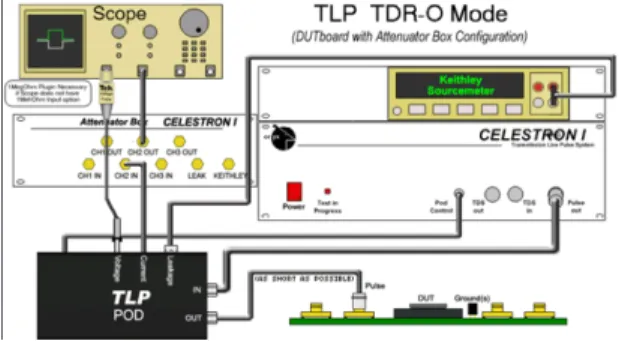
All the PCB lines are 50Ω impedance. The pattern allows both measurement and injection techniques. The discharge from SMA_injection can be modulated with external elements placed on footprints 1 to 5. The capacitor under study is placed on footprint 3. A dedicated calibration pattern is placed on the board to calibrate each configuration used during the tests. SMA_CH3 allows the voltage measurement by adding a 500 Ω resistance on footprint 6. Using such resistance value, in parallel to the 50 Ω lines, we get an attenuation of 21dB. This on-board dedicated probe has been characterized in the frequency domain using VNA and exhibited a good linearity up to 1GHz. All measurements in this article are made using a TLP-TDR (Time Domain Reflectometry) generator with 1ns rise time and 100ns duration. The setup is reported in figure 2. The equipment under test could be one of the two boards or directly the standalone capacitor. The “Celestron” box is the TLP generator, the “TLP POD” is a TDR box that allows the measurement of injected and reflected pulses. An attenuator is used to protect the 6GHz bandwidth oscilloscope. It means that we perform both voltage measurement at board level, and voltage and current measurement using TDR method. In this paper we started to analyze how the capacitance behaves in the system configuration (on the LIN board). The TLP-TDR is used secondly to precisely extract the model of the capacitor. In this case the TLP injection is directly done at the standalone capacitor.
Fig. 2. TLP-TDR measurement setup.
3. Impacts of non-linear X7R capacitance. A. Observations
The figure 3 presents voltage measurements of 1nF (a) and 10nF (b) capacitors connected to the LIN input (Lin board). In our case, the on-chip protection is a snapback device that triggers at 70V with a holding voltage of 17V. It shows two different behaviors. These capacitors are compared to a C0G capacitor with a constant value during stresses. In two cases the voltage through the capacitor reaches 70V (triggering condition of the component). Compared to the C0G charged voltage, the behavior of the two X7R capacitors is completely different. With the 1nF capacitor, the X7R is charging more slowly than the C0G type. This is completely the opposite for the 10nF capacitor.
It results in the modification of triggering time of the on-chip protection. In case (a), the C0G type triggers the protection. In case (b), the X7R triggers the protection.
Such behavior is not predictable using standard capacitor model into simulation (the C0G type respect a basic model). To be able to predict soft errors, such differences have to be taken into account in simulations, and a methodology to extract the behavior of the X7R capacitance is needed.
(a) 1nF capacitances, 100V TLP injection
(b) 10nF capacitances, 400V TLP injection
Fig. 3. Comparison between C0G and X7R capacitors, in parallel with LIN component.
B. Capacitance model extraction.
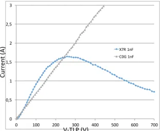
Using TLP-TDR, a quasi static I(V) curve is obtained for each tested capacitor: C0G and X7R. Results of the 1nF capacitances are reported in Figure 4. The X-coordinate is the pre-charged voltage of the TLP generator. The current points reported correspond to the reflected values obtained at 80ns. As shown, the C0G type is purely linear and respects the charge law of a 1nF capacitance. Regarding the X7R, from 0 to 200V TLP, the current through the capacitor is higher than the C0G one then it continuously decreases as the C0G one continues to increase. Looking at TLP response it looks like two different components.
0 0,5 1 1,5 2 2,5 3 0 100 200 300 400 500 600 700 X7R,1nF C0G,1nF Cur re nt '(A )' V,TLP'(V)'
Fig. 4: TLP measurements of 1nF capacitances C0G and X7R type.
From this result a C(V) curve is extracted using the charge capacitance formula.
Where Icapa(t) is the measured current, V_TLP, the charge voltage of the TLP generator and TAU the time constant of the RC network. t is the time where the I(V) measurement is performed minus the time to get the reflection (10ns). We assumed that R=50Ω because all the setup is 50Ω impedance. From the transient waveforms (fig.5) we can extract the value of the capacitance depending in the injection voltage.
Figure 5. Transient waveforms of voltage and current reflected pulses for 100V TLP injection on 1nF
capacitance.
For X7R we compute the value of the capacitance obtained during TLP stress at 20ns, 40ns and 70ns versus TLP stress. The results are reported in figure 6. It seems that the modification of the capacitance value depends on the stress time. At 20ns, only a small variation around the 1nF is observed. At 70ns, the variation is more important and reaches 0.5nF for the 1nF nominal value. 0 0,2 0,4 0,6 0,8 1 1,2 0 200 400 600 800 c=f(vtlp)1@20ns c=f(vtlp)1@40ns c=f(vtlp)1@70ns Cap ac itan ce )(n F) ) V.TLP)(V))
Fig. 6: Computed X7R capacitance value versus TLP stress at t= 20ns, 40ns and 70ns.
From the data of figure 6, we could think that the capacitance value depends on the stress time. To validate this assumption, we report in figure 7 the computed capacitance versus the voltage across the X7R. 0 0,2 0,4 0,6 0,8 1 1,2 0 200 400 600 800 c=f(vcapa)0@20ns c=f(vcapa)0@40ns c=f(vcapa)0@70ns Cap ac itan ce )(n F) ) V.Capacitance)(V))
Fig. 7: Computed X7R capacitance value versus voltage across the capacitor at t= 20ns, 40ns and 70ns.
Now, the evolution of the capacitance is almost the same for each stress time. This result demonstrates that the capacitance value depends on the voltage between its pins.
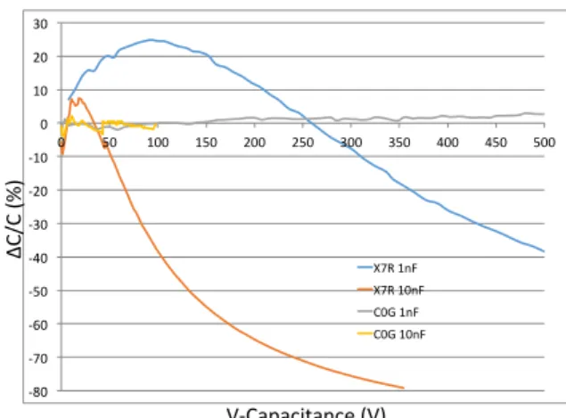
The figure 8 reports the percentage of variation of each capacitance type (X7R and C0G) versus the TLP stress amplitude for the 1nF and 10nF capacitances. As expected, there is no variation on the C0G capacitance. For X7R, the nominal value increases for small TLP stress injection (less than 300V) up to 20%. After 300V TLP it decreases to around 50% of its value for the 1nF and 80% for the 10nF. The behavior of the two capacitances looks similar.
Figure 9 reports the nominal value of the capacitance depending on the voltage at its pins (note that it is a transient voltage). As noticed, this voltage is much more higher than the one provided by the datasheet. This representation clearly shows that the 1nF and the 10nF (same provider) have a very different behavior. This phenomenom can explain the differences observed into the transient waveforms of figure 3. For 100V injection on the 1nF and 400V injection on the 10nF, the voltage across the capacitors reaches 70V. Looking at figure 8, 1nF capacitor exhibits a 20% increase that slows down the charge (Fig.3(a)). The 10nF has decreased by 20% that explains the rapid charge observed in figure 3(b)
!80$ !70$ !60$ !50$ !40$ !30$ !20$ !10$ 0$ 10$ 20$ 30$ 0$ 100$ 200$ 300$ 400$ 500$ 600$ 700$ 800$ X7R$1nF$ X7R$10nF$ C0G$1nF$ C0G$10nF$ ∆C/C$(% )$ V)TLP$(V)$
Fig. 8. C(V) of the 1nF, 10nF capacitance C0G and X7R versus amplitude of the TLP stress
!80$ !70$ !60$ !50$ !40$ !30$ !20$ !10$ 0$ 10$ 20$ 30$ 0$ 50$ 100$ 150$ 200$ 250$ 300$ 350$ 400$ 450$ 500$ X7R$1nF$ X7R$10nF$ C0G$1nF$ C0G$10nF$ V"Capacitance+(V)+ ∆C/C+(% )+
Fig. 9. C(V) of the 1nF, 10nF capacitance C0G and X7R vs transient voltage over the capacitance. We also investigated if the rise time of the pulse could have an influence. Three rise times have been used: 175ps, 1ns and 10ns. The pulse duration is fixed to 100ns. As shown in figure 10, there is not impact.
0 2E$10 4E$10 6E$10 8E$10 1E$09 1,2E$09 1,4E$09 0 100 200 300 400 500 600 700 800 C=f(VTLP)7tr=175ps C=f(VTLP)77tr=1ns C=f(VTLP)7tr=10ns
Cap
ac
itan
ce
)(F
))
V.VTLP)(V))
0 2E$10 4E$10 6E$10 8E$10 1E$09 1,2E$09 1,4E$09 0 100 200 300 400 500 600 700 800 C=f(VTLP)7tr=175ps C=f(VTLP)77tr=1ns C=f(VTLP)7tr=10nsFig. 10: Computed X7R (1nF) capacitance value versus TLP voltage stress for diferent rise time : 175ps, 1ns and 10 ns.
As mentionned in this chapter, depending on the type of capacitor, important modifications of the nominal value can be observed during ESD stresses. For X7R, up to 80% capacitance value variation is observed. We proposed a way to get this value using TLP. Such important modification of the capacitance must be taken into account into the simulations. From the measurements we built VHDL-AMS models of the capacitances and insert it into the simulation. The model is based on a polynomial expression. The expression obtained for the 1nF is reported below:
4. Simulation and measurement comparison
The whole measurement setup is reproduced in simulation. Following the methodology presented in most papers dealing with SEED, behavioral models are created with quasi-static measurements obtained by a 100 ns, 1ns rise time TLP injection. The component’s pins are tested in pairs with positive and negative pulses.
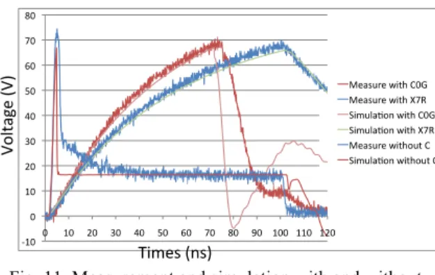
The X7R are modeled using a polynomial equation, the C0G is represented with an ideal capacitance. For each capacitance model, a high frequency part is added with its parasitic elements (RLC) extracted using a vector network analyzer (VNA). The simulation results with and without the 1nF capacitor, compared with measurement data are reported in figure 11. The charge is perfectly reproduced, for both C0G and X7R capacitors.The impact of the introduced delay to trigger the protection is well predicted.
The discharge exhibits an on-chip resistance not modelled into the IC model. It appears that complex transient phenomena control the discharge. This is not related to the capacitor (C0G) in this case but to the internal IC behavior. The way to model the transient turn-on of the protection is studied in article [9] where a dedicated measurement method is provided to extract dynamic on-chip parameters.
As shown in Fig. 12, the shape of the voltage is not well reproduced in the simulation with the 10 nF X7R, i.e. the variation of the capacitance is much more important than the model extracted. Additional expertise is needed to understand why the behavior of the capacitor is not the one reported Fig. 9.
!10$ 0$ 10$ 20$ 30$ 40$ 50$ 60$ 70$ 80$ 0$ 10$ 20$ 30$ 40$ 50$ 60$ 70$ 80$ 90$ 100$ 110$ 120$ Measure$with$C0G$ Measure$with$X7R$ Simula>on$with$C0G$ Simula>on$with$X7R$ Measure$without$C$ Simula>on$without$C$ Vo ltag e( (V )( Times((ns)(
Fig. 11. Measurement and simulation with and without capacitor (1nF) for the LIN component, 100V TLP
injection
5. Conclusion
Highly accurate system modeling is required to achieve system ESD soft failure prediction. The external elements have a great impact on the on-chip phenomenon. The paper investigates the non-linearity
of X7R capacitors and the impact on transient response. We demonstrated that during ESD stresses, capacitances could have strong variations up to 80% of their nominal value. Such important variations must be taken into account in simulation. We show that this variation is mainly related to the voltage across the capacitor. Using TLP, a method to extract the evolution of that capacitance is presented for modeling purpose. A new model of the capacitor is introduced into the simulation that provides an accurate prediction of the in-situ measured waveform. This method has been applied to X7R capacitors, and it can be used to extract any other types of capacitor.
is much more important than the model extracted. Additional expertise is needed to understand why the behavior of the capacitor is not the one reportedFig. 9.
5. Conclusion
Highly accurate system modeling is required to achieve system ESD soft failure prediction. The external elements have a great impact on the on-chip phenomenon. The paper investigates the non-linearity of X7R capacitors and the impact on transient response. We demonstrated that during ESD stresses, capacitances could have strong variations up to 80% of their nominal value. Such important variations must be taken into account in simulation. We show that this variation is mainly related to the voltage across the capacitor. Using TLP, a method to ex-tract the evolution of that capacitance is presented for modeling pur-pose. A new model of the capacitor is introduced into the simulation that provides an accurate prediction of the in-situ measured waveform. This method has been applied to X7R capacitors, and it can be used to extract any other types of capacitor. If the variation of the capacitance
is not too significant. New extraction method is being investigated to develope a model for highly variation of capacitance.
Acknowledgement
The authors would like to thank the French National Agency of Re-search (ANR) for its financial support on the project EFT-SAFE3A (EFT Safe Automotive, Aeronautic applications). The authors would also like to address their thanks to the ESDA, WG26 (models for system level simulation) working group for their support on the boards and discus-sions on this topic.
References
[1] Industry Council on ESD Target Levels, White paper “System Level ESD, Part I: Com-mon Misconceptions and Recommended Basic Approaches”.
[2]N. Monnereau, F. Caignet, D. Tremouilles, Building-up of System Level ESD Modeling: Impact of a Decoupling Capacitance on ESD Propagation, Electrical Overstress/Elec-trostatic Discharge Symposium (EOS/ESD), 2010 1–10 (3–8 Oct. 2010). [3]N. Monnereau, F. Caignet, N. Nolhier, D. Trémouilles, M. Bafleur, Behavioral-Modeling
Methodology to Predict Electrostatic-Discharge Susceptibility Failures at System Level: An IBIS Improvement, EMC Europe Symposium, sept. 2011.
[4]N. Monnereau, F. Caignet, N. Nolhier, et al., Investigation of modeling system ESD fail-ure and probability using IBIS ESD models, IEEE Trans. Device Mater. Reliab. 12 (4) (Dec. 2012) 599–606.
[5]L. Tianqi, et al., An application of utilizing the system-efficient-ESD-design (SEED) concept to analyze an LED protection circuit of a cell phone, Electromagnetic Compat-ibility (EMC), 2012 IEEE International Symposium, 2012.
[6]R. Mertens, E. Rosenbaum, H. Kunz, A. Salman, G. Boselli, A flexible simulation model for system level ESD stresses with applications to ESD design and troubleshooting, 34rd Electrical Overstress/Electrostatic Discharge Symposium (EOS/ESD), 2012. [7]C. Reiman, N. Thomson, X. Yang, R. Mertens, E. Rosenbaum, “Practical Methodology
for the Extraction of SEED Models”, Electrical Overstress/Electrostatic Discharge Sym-posium (EOS/ESD), 2015.
[8]Hongyu Li, Victor Khilkevich, Tianqi Li, David Pommerenke, Seongtae Kwon, Wesley Hackenberger, “Nonlinear capacitors for ESD protection”, IEEE Electromagn. Compat. Mag. 1 (4) (Dec. 2012) 38–46.
[9]F. Escudié, F. Caignet, N. Nolhier, M. Bafleur, From quasi-static to transient system level ESD simulation: extraction of non-linear turn-on elements, 38rd Electrical Over-stress/Electrostatic Discharge Symposium (EOS/ESD), 2016.
Fig. 12. Measurement and simulation with capacitor (10 nF) for the LIN component, 400 V TLP injection.
5 F. Escudié et al. / Microelectronics Reliability xxx (2016) xxx–xxx
Please cite this article as: F. Escudié, et al., Impact of non-linear capacitances on transient waveforms during system level ESD stress, Microelec-tronics Reliability (2016),http://dx.doi.org/10.1016/j.microrel.2016.07.046
Fig. 12. Measurement and simulation with capacitor (10nF) for the LIN component A, 400V TLP injection
Acknowledgement
The authors would like to thank the French National Agency of Research (ANR) for its financial support on the project EFT-SAFE3A (EFT Safe Automotive, Aeronautic applications). The authors would also like to address their thanks to the ESDA, WG26 (models for system level simulation) working group for their support on the boards and discussions on this topic.
References
[1] Industry Council on ESD Target Levels, White Paper "System Level ESD, Part I: Common Misconceptions and Recommended Basic Approaches”.
[2] N. Monnereau, F. Caignet, D. Tremouilles, "Building-up of system level ESD modeling: Impact of a decoupling capacitance on ESD propagation, Electrical Overstress/ Electrostatic Discharge Symposium (EOS/ESD), 2010, pp.1-10, 3-8 Oct. 2010
[3] N. Monnereau, F. Caignet, N, Nolhier, D. Trémouilles, M. Bafleur, "Behavioral-Modeling Methodology to Predict Electrostatic-Discharge Susceptibility Failures at System Level : an IBIS Improvement" EMC Europe Symposium, sept. 2011.
[4] N. Monnereau, F. Caignet, N. Nolhier, et al., “Investigation of Modeling System ESD Failure and Probability Using IBIS ESD Models”, IEEE Trans. on Device and Materials Reliability, Volume: 12 Issue: 4 Pages: 599-606, Dec. 2012.
[5] Tianqi Li; et al., “An application of utilizing the system-efficient-ESD-design (SEED) concept to analyze an LED protection circuit of a cell phone,” Electromagnetic Compatibility (EMC), 2012 IEEE International Symposium. [6] R. Mertens, E. Rosenbaum, H. Kunz, A. Salman, and G. Boselli, “A flexible simulation model for system level ESD stresses with applications to ESD design and troubleshooting,” 34rd Electrical Overstress/Electrostatic Discharge Symposium (EOS/ESD), 2012.
[7] Collin Reiman, Nicholas Thomson, Yang Xiu, Robert Mertens and Elyse Rosenbaum, “Practical Methodology for the Extraction of SEED Models”, Electrical Overstress/ Electrostatic Discharge Symposium (EOS/ESD), 2015. [8] Hongyu Li, Victor Khilkevich, Tianqi Li, David
Pommerenke, Seongtae Kwon, Wesley Hackenberger, “Nonlinear capacitors for ESD protection”, IEEE Electromagnetic Compatibility Magazine, Volume:1, Issue: 4, Page(s):38 – 46.
[9] Fabien Escudié, Fabrice Caignet, Nicolas Nolhier, Marise Bafleur, “From Quasi-static to Transient System Level ESD Simulation: Extraction of Non-linear Turn-on Elements”, 38rd Electrical Overstress/Electrostatic Discharge Symposium (EOS/ESD), 2016.