HAL Id: tel-01332949
https://tel.archives-ouvertes.fr/tel-01332949
Submitted on 16 Jun 2016
HAL is a multi-disciplinary open access
archive for the deposit and dissemination of
sci-entific research documents, whether they are
pub-lished or not. The documents may come from
teaching and research institutions in France or
abroad, or from public or private research centers.
L’archive ouverte pluridisciplinaire HAL, est
destinée au dépôt et à la diffusion de documents
scientifiques de niveau recherche, publiés ou non,
émanant des établissements d’enseignement et de
recherche français ou étrangers, des laboratoires
publics ou privés.
System-Level Hardwa Synthesis of Dataflow Programs
with HEVC as Study Use Case
Mariem Abid
To cite this version:
Mariem Abid. System-Level Hardwa Synthesis of Dataflow Programs with HEVC as Study Use Case.
Signal and Image Processing. INSA de Rennes; École nationale d’ingénieurs de Sfax (Tunisie), 2016.
English. �NNT : 2016ISAR0002�. �tel-01332949�
THESE INSA Rennes
sous le sceau de l’Université Bretagne Loire pour obtenir le titre de DOCTEUR DE L’INSA RENNES Spécialité : Traitement du Signal et de l`imageprésentée par
Mariem Abid
ECOLE DOCTORALE : MATISSE LABORATOIRE : IETRSystem-Level Hardware
Synthesis of dataflow
programs with HEVC as
study use case
Thèse soutenue le 28.04.2016
devant le jury composé de :
Mohamed Akil
Professeur à l’ESIEE Paris (France) / Président et Rapporteur
Ahmed Chiheb Ammari
Associate Professor à Université du roi Abdulaziz à Jeddah (Arabie Saoudite) / Rapporteur
Mohamed Atri
Maître de Conférences à Faculté des Sciences de Monastir (Tunisie) / Examinateur
Audrey Queudet
Maître de conférences à l’université de Nantes (France) / Examinateur
Olivier Déforges
Professeur à l’INSA de Rennes (France) / Directeur de thèse
Mohamed Abid
Professeur à l’Ecole Nationale d’Ingénieur de Sfax (Tunisie) / Directeur de thèse
System-Level Hardware
Synthesis of Dataflow
Programs with HEVC as
Study Use Case
Mariem Abid
En partenariat avec
Dedication
i
To the loving memory of my mother,
Taicir,
who has made me the person I am becoming.
To my father,
Najib,
who has been my role-model for hard work.
To my sister,
Mona,
who has been my emotional anchor.
To my husband,
Hamza,
who has shared the many sacrifices for completing this dissertation.
To my son,
Elyes,
who is my lucky charm.
Abstract
Image and video processing applications are characterized by the processing of a huge amount of data. The design of such complex applications with traditional design methodologies at low-level of abstraction causes increasing development costs. In order to resolve the above mentioned challenges, Electronic System Level (ESL) synthesis or High-Level Synthesis (HLS) tools were proposed. The basic premise is to model the behavior of the entire system using high-level specifications, and to enable the automatic synthesis to low-level specifications for efficient im-plementation in Field-Programmable Gate Array (FPGA). However, the main downside of the HLStools is the lack of the entire system consideration, i.e. the establishment of the communi-cations between these components to achieve the system-level is not yet considered.
The purpose of this thesis is to raise the level of abstraction in the design of embedded sys-tems to the system-level. A novel design flow was proposed that enables an efficient hardware implementation of video processing applications described using a Domain Specific Language (DSL) for dataflow programming. The design flow combines a dataflow compiler for generating
C-basedHLSdescriptions from a dataflow description and a C-to-gate synthesizer for generating Register-Transfer Level (RTL) descriptions. The challenge of implementing the communication channels of dataflow programs relying on Model of Computation (MoC) inFPGAis the mini-mization of the communication overhead. In this issue, we introduced a new interface synthesis approach that maps the large amounts of data that multimedia and image processing applica-tions process, to shared memories on the FPGA. This leads to a tremendous decrease in the latency and an increase in the throughput. These results were demonstrated upon the hardware synthesis of the emerging High-Efficiency Video Coding (HEVC) standard.
R´esum´e
Les applications de traitement d’image et vid´eo sont caractris´ees par le traitement d’une grande quantit´e de donn´ees. La conception de ces applications complexes avec des m´ethodologies de con-ception traditionnelles bas niveau provoque l’augmentation des coˆuts de d´eveloppement. Afin de r´esoudre ces d´efis, des outils de synth`ese haut niveau ont ´et´e propos´es. Le principe de base est de mod´eliser le comportement de l’ensemble du syst`eme en utilisant des sp´ecifications haut niveau afin de permettre la synth`ese automatique vers des sp´ecifications bas niveau pour impl´ementation efficace enFPGA. Cependant, l’inconv´enient principal de ces outils de synth`ese haut niveau est le manque de prise en compte de la totalit´e du syst`eme, c.-`a-d. la cr´eation de la communication entre les diff´erents composants pour atteindre le niveau syst`eme n’est pas consid´er´ee.
Le but de cette th`ese est d’´elever le niveau d’abstraction dans la conception des syst`emes em-barqu´es au niveau syst`eme. Nous proposons un flot de conception qui permet une synth`ese mat´erielle efficace des applications de traitement vid´eo d´ecrites en utilisant un langage sp´ecifique `
a un domaine pour la programmation flot-de-donn´ees. Le flot de conception combine un compi-lateur flot-de-donn´ees pour g´en´erer des descriptions `a base de code C et d’un synth´etiseur pour g´en´erer des descriptions niveau de transfert de registre. Le d´efi majeur de l’impl´ementation en FPGAdes canaux de communication des programmes flot-de-donn´ees bas´es sur un mod`ele de calcul est la minimisation des frais g´en´eraux de la communication. Pour cel`a, nous avons introduit une nouvelle approche de synth`ese de l’interface qui mappe les grandes quantit´es des donn´ees vid´eo, `a travers des m´emoires partag´ees surFPGA. Ce qui conduit `a une diminution consid´erable de la latence et une augmentation du d´ebit. Ces r´esultats ont ´et´e d´emontr´es sur la synth`ese mat´erielle du standard vid´eo ´emergent High-Efficiency Video Coding (HEVC).
Acknowledgment
iii
“ You gave me your time, the most thoughtful gift of all”
Dan Zadra
Firstly, I would like to express my sincere gratitude to my thesis directors Prof. Mohamed Abid
and Prof. Olivier Déforges. My special recognition goes out to Prof. Mohamed Abid who gave
me the opportunity to join the ENIS-CES Lab and offered me the wonderful research
opportunity to join INSA-IETR Lab through
a cotutelle agreement. My sincere appreciation and gratitude to Prof. Olivier Déforges for the
continuous support of my Ph.D study, for his patience, motivation, and immense knowledge. His
guidance helped me in all the time of research and writing of this thesis. Thank you very much to
both of you for your human exchange and for understanding and considering my personal
.
Besides, I would like to thank my advisor Dr. Mickael Raulet, for his guidance, for all the
invested time in the supervision of my thesis and for his readiness for listening to the little
problems and roadblocks that unavoidably crop up in the course of performing research. In
addition, I acknowledge the very interesting theme he proposed for my thesis and the critical
comments on this written work.
Besides my advisors, I would like to thank the jury members: Mr Ahmed Chiheb Ammari, Mr
Mohamed Akil, Mr Mohamed Atri and Mrs Audrey Queudet, for honouring my jury, for their
precious time reading my thesis defense and for their constructive comments.
I am grateful to my fellow labmates of the image team, Khaled, Hervé, Alexandre, Gildas and
Antoine for helping me solving the problems in research. Also I thank my friends in the CES Lab
for the scientific discussions and for helping me in the administration issues.
A special thought to Mrs Jocelyne Tremier, Mrs Corinne Calo and Mrs Aurore Gouin for their
administrative support in the INSA of Rennes and
.
Contents
List of Figures ix
List of Tables xi
Acronyms xv
1 Introduction 1
1.1 Context and Motivation . . . 1
1.2 Problem Statement and Contributions . . . 2
1.3 Outline . . . 3
1.4 Publications . . . 3
I
BACKGROUND
5
2 Fundamentals of Embedded Systems Design 7 2.1 Introduction . . . 72.2 The Embedded Systems Design . . . 7
2.2.1 What is an embedded system? . . . 7
2.2.1.1 What is an Application-Specific Integrated Circuit (ASIC)? . . . 8
2.2.1.2 What is a Field-Programmable Gate Array (FPGA)? . . . 8
2.2.2 Video compression inFPGA . . . 9
2.2.3 The embedded systems design challenges . . . 10
2.2.3.1 Design constraints . . . 10
2.2.3.2 Design productivity gap . . . 11
2.3 Hardware Design Methodologies . . . 11
2.3.1 Levels of abstraction . . . 12
2.3.2 Bottom-up methodology . . . 13
2.3.3 Top-down methodology . . . 13
2.3.4 System design process . . . 13
2.3.5 Design flow and taxonomy of synthesis . . . 14
2.4 Register-Transfer Level (RTL) Design . . . 15
2.4.1 What is a Hardware Description Language (HDL)? . . . 16
2.4.2 What is wrong withRTLdesign andHDLs? . . . 17
2.5 High-Level Synthesis (HLS) Design . . . 18
2.6 System-Level Design . . . 22
2.7 Conclusion . . . 24
Bibliography 27 3 Dataflow Programming in the Reconfigurable Video Coding (RVC) Frame-work 33 3.1 Introduction . . . 33
3.2 Dataflow Programming . . . 33
3.3 TheRVCStandard . . . 35
3.3.1 Motivation and Objectives . . . 35
3.3.2 Structure of the Standard . . . 35
3.3.3 Instantiation Process of aRVCAbstract Decoder Model (ADM) . . . 36
3.4 RVC-Caltrop Actor Language (CAL) Dataflow Programming . . . 37 v
CONTENTS vi
3.4.1 RVC-CALLanguage . . . 37
3.4.2 Representation of Different Model of Computations (MoCs) inRVC-CAL 39 3.5 RVC-CALCode Generators and Related Work . . . 42
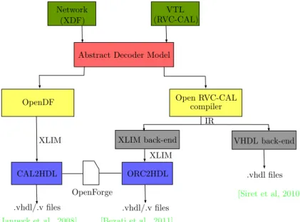
3.5.1 Open Dataflow environment (OpenDF) . . . 42
3.5.2 OpenRVC-CALCompiler (Orcc) . . . 43
3.6 Conclusion . . . 45
Bibliography 47
II
CONTRIBUTIONS
51
4 Toward Efficient Hardware Implementation of RVC-based Video Decoders 53 4.1 Introduction . . . 534.2 Limitations of the Current Solution and Problem Statement . . . 53
4.3 Rapid Prototyping Methodology . . . 55
4.3.1 Outline of the Prototyping Process . . . 55
4.3.2 System-Level Synthesis usingOrcc . . . 57
4.3.2.1 VivadoHLSCoding Style . . . 57
4.3.2.2 Automatic Communication Refinement . . . 58
4.3.2.3 Automatic Computation Refinement . . . 59
4.3.3 HLSusing VivadoHLS . . . 61
4.3.4 System-Level Integration . . . 62
4.3.5 Automatic Validation . . . 62
4.4 Rapid Prototyping Results: High-Efficiency Video Coding (HEVC) Decoder Case Study . . . 63
4.4.1 RVC-CALImplementation of theHEVCDecoder . . . 63
4.4.1.1 TheHEVCstandard . . . 63
4.4.1.2 TheRVC-CAL HEVCDecoder . . . 66
4.4.1.3 Test Sequences . . . 66
4.4.2 Optimization Metrics . . . 68
4.4.3 Experimental Setup . . . 68
4.4.4 Experimental Results . . . 69
4.4.4.1 The Main Still Picture profile ofHEVCcase study . . . 69
4.4.4.2 The IntraPrediction Functional Unit (FU) Case Study . . . 71
4.4.4.3 Design-Space Exploration (DSE) Through Optimizations Direc-tives . . . 71
4.5 Conclusion . . . 73
Bibliography 75 5 Toward Optimized Hardware Implementation of RVC-based Video Decoders 77 5.1 Introduction . . . 77
5.2 Issues with Explicit Streaming . . . 78
5.3 Interface Synthesis Optimization . . . 79
5.3.1 Shared-Memory Circular Buffer . . . 79
5.3.2 Scheduling Optimization . . . 81
5.3.3 Synthesis of Arrays . . . 82
5.3.4 System-Level Integration . . . 83
5.3.5 Test Infrastructure . . . 85
5.4 Experimental Results . . . 85
5.4.1 The Main Still Picture profile ofHEVCcase study . . . 85
5.4.2 The Main profile ofHEVCcase study . . . 86
5.4.2.1 Throughput Analysis . . . 87
5.4.2.2 Latency Analysis . . . 88
5.4.3 Task Parallelism Optimization . . . 89
5.4.4 Data parallelism optimization . . . 90
5.4.4.1 YUV-ParallelRVC-CAL HEVCdecoder . . . 90
CONTENTS vii
5.4.5 Comparison with Other Works . . . 92
5.4.5.1 System-level hardware synthesis versus hand-coded HDLof the HEVCdecoder . . . 92
5.4.5.2 Comparison with other alternativeHLSforRVC-CAL . . . 92
5.5 Conclusion . . . 93
Bibliography 95 6 Conclusion 97
III
APPENDIX
101
Appendix A System-Level Design Flow: Tutorial 103 A.1 A User Guide for the C-HLSBackend: Steps and Requirements . . . 103A.2 Write a Very Simple Network . . . 103
A.2.1 Setup a NewOrccProjet . . . 103
A.2.2 Implements Actors . . . 103
A.2.3 Build theOrccNetwork . . . 106
A.3 Compile RVC-CALProgram Using the C-HLSBackend . . . 107
A.4 Compile the C-HLScode to Very High-Speed Integrated Circuits (VHSIC) Hard-ware Description Language (VHDL) with VivadoHLS . . . 108
A.5 Synthesize the VHDLUsing Xilinx ISE . . . 108
Appendix B HEVCTest Sequences 111 Appendix C Summary of Vivado HLS directives 113 Appendix D R´esum´e en fran¸cais 115 D.1 Contexte et Motivation . . . 115
D.2 ´Enonc´e du probl`eme et contributions . . . 116
D.3 Organisation du rapport de th`ese . . . 117
D.4 ´Etat de l’art . . . 118
D.4.1 Le paradigme de programmation flot-de-donn´ees . . . 118
D.4.2 La norme Moving Picture Experts Group (MPEG)-RVC . . . 118
D.4.3 Le langage de programmation flot-de-donn´eesRVC-CALet son mod`ele de calcul . . . 119
D.4.4 Travaux connexes en g´en´eration de code HDL `a partir de programmes RVC-CAL . . . 120
D.4.4.1 Conception au niveau composant . . . 120
D.4.4.2 Conception au niveau syst`eme . . . 120
D.5 Pr´esentation du flot de conception niveau syst`eme propos´e . . . 121
D.6 Probl´ematique du flot de conception propos´e . . . 123
D.7 Optimization de l’interface de communication . . . 123
D.8 Cas d’´etude: le d´ecodeurHEVC. . . 124
D.9 Conclusion et perspectives . . . 125
List of Figures
2.1 The basic FPGA structure: a logic block consists of a 4-input Look-up table
(LUT), and a Flip-Flop (FF). . . 8
2.2 Hybrid video encoder [Jacobs and Probell,2007]. . . 9
2.3 Difference between design complexity and design productivity: the productivity gap. Source: Sematech1 . . . 11
2.4 Gajski-Kuhn Y-chart. . . 12
2.5 Different representations of the main components at each abstraction level. . . . 13
2.6 Design methodologies in the Y-chart. . . 14
2.7 Major steps in the embedded systems design process [Wolf,2008]. . . 14
2.8 The evolution of design methodology adoption in the Electronic Design Automa-tion (EDA) industry2. . . . 15
2.9 The path of the first, second and thirdEDAgenerations in the Y-chart. . . 16
2.10 RTLschematic of the 1-bit half adder (logic synthesis with Xilinx ISE). . . 17
2.11 Gasjki-Kuhn Y-Chart forHLSDesign Flow. . . 18
2.12 Steps of HLS[Andriamisaina et al.,2010]. . . 19
2.13 Relation between abstraction and synthesis levels [Teich,2000]. . . 22
2.14 Gasjki-Kuhn Y-Chart for System-level Design Flow. . . 22
2.15 System-Level Synthesis. . . 22
2.16 A methodology toDSEat the system-level [Kienhuis et al.,1997]. . . 24
3.1 A dataflow graph containing five components interconnected using communication channels. . . 33
3.2 The first dataflow representation as introduced by Sutherland in 1966 [Sutherland, 1966]. . . 34
3.3 Modularity in dataflow graph. . . 35
3.4 RVCnetwork example. . . 36
3.5 The conceptual process of deriving a decoding solution by means of normative and nonnormative tools in theRVCframework [Mattavelli et al.,2010]. . . 37
3.6 Scheduling information and body of an action. . . 38
3.7 Pictorial representation of the RVC-CAL dataflow programming model [Amer et al.,2009]. . . 40
3.8 Classification of dataflowMoCs with respect to expressiveness and analyzability [Wipliez and Raulet,2010]. . . 40
3.9 Non-standard tools for the automatic hardware code generation in theRVC frame-work. . . 43
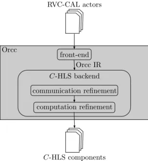
3.10 Compilation infrastructure of Orcc[Wipliez,2010]. . . 44
4.1 The compilation flow of the XML Language-Independent Model (XLIM) back-end [Bezati et al., 2011]. . . 54
4.2 Automatic Multi-to-Mono (M2M) tokens transformation localization in the hard-ware generation flow [Jerbi et al.,2012]. . . 54
4.3 Our proposed system-level design flow. . . 56
4.4 System-level synthesis stage (a) of Figure4.3. . . 56
4.5 HLSstage (b) of Figure4.3. . . 57
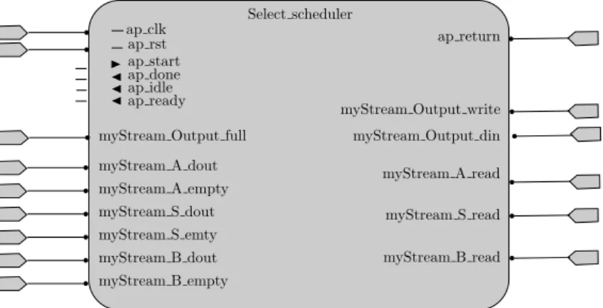
4.6 The correspondingRTLimplementation of the interface ports of the actor Select using explicit streaming. . . 61
4.7 Timing behavior of ap fifo interfaces port of the actor Select. . . 61
4.8 System-level elaboration using explicit streaming. . . 63
4.9 HEVCencoder/decoder. . . 64 ix
LIST OF FIGURES x
4.10 Top-levelRVC FUNetwork Language (FNL) description of theHEVCdecoder. . 66
4.11 The RVC FNLdescription of theHEVCDecoderFU. . . 67
4.12 Implementation flow. . . 69
4.13 Decoded HEVCvideo sequences used in experiments. . . 70
5.1 The Finite-State Machine (FSM) of the Transpose32× 32 actor. . . . 78
5.2 Conceptual view of a circular buffer. . . 80
5.3 A shared-memory circular buffer used to mediate communication between actors with respect to the Dataflow Process Network (DPN) semantics. . . 80
5.4 The correspondingRTLimplementation of the interface ports of the actor Select using implicit streaming. . . 83
5.5 Timing behavior of ap memory interface ports of the actor Select. . . 83
5.6 The Random-Access Memory (RAM) component implementation. . . 84
5.7 Gantt-chart of the HEVC Inter Decoder. . . 87
5.8 Latency bottleneck analysis using Gantt-chart. . . 89
5.9 Refactoring of the xIT actor. . . . 89
5.10 Example of the YUV-parallel split of the IntraPredictionFU. . . 90
5.11 Graphical representation of the actors behavior of the YUV design simulation: The frame decoding start and end times are recorded for each actor during the system simulation for an image sequence of 5 frames. . . 91
5.12 RVC-CALdescription of theMPEG-4 Simple Profile (SP) decoder. . . 92
A.1 Step 1: How to create a new Orccproject. . . 104
A.2 Step 1: Source code of actors to implement inRVC-CAL. . . 105
A.3 Step 1: How to build anOrccnetwork. . . 106
A.4 Step 1: How to build anOrccnetwork. . . 107
A.5 Step 2: How to run an eXtensible Markup Language (XML) Dataflow Format (XDF) network using the C-HLSbackend. . . 107
A.6 Step 2: Compilation console output. . . 107
A.7 Step 2: Content of the output folder HLSBackend. . . 108
A.8 Step 3: Files resulting from hardware synthesis. . . 109
A.9 Step 4: How to Synthesize theVHDLUsing Xilinx ISE. . . 109
A.10 Step 4: How to Synthesize theVHDLUsing Xilinx ISE. . . 109
D.1 La norme RVC: La partie sup´erieure est le processus standard d’´elaboration d’une sp´ecification abstraite, la partie inf´erieure est le processus non-standard de g´en´eration des impl´ementations multi-cibles `a partir de la sp´ecification standard.118 D.2 Un mod`eleDPNest con¸cu comme un graphe orient´e compos´e de sommets (c.-`a-d. acteurs) et les bords repr´esentent des canaux de communication unidirectionnels bas´es sur le principe First-In First-Out (FIFO). . . 119
D.3 Les diff´erents niveaux d’abstraction. . . 120
D.4 Flot de conception niveau syst`eme propos´e. . . 122
D.5 Impl´ementation mat´erielle de laFIFO. . . 122
D.6 Impl´ementation mat´erielle de laRAM. . . 123
D.7 DescriptionRVC CAL au plus haut niveau du decodeurHEVC. . . 125
List of Tables
2.1 Truth table of half adder. . . 17 4.1 By default allHLSgenerated designs have a master control interface. . . 62 4.2 Characteristics of theFUs of the HEVCDecoderFU. . . 67 4.3 Time results for the RVC-CAL HEVC decoder (Main Still Picture profile)
sim-ulated by the Stream Design for 3 frames of the BQSquare video sequence at 50MHz. . . 70 4.4 Maximum operating frequency and area consumption for the SelectCU and
IntraPrediction FUs of the RVC-CAL HEVC decoder (Main Still Picture profile) synthesized by the Stream Design for 3 frames of the BQSquare video sequence on a Xilinx Virtex 7 platform (XC7V2000T) at 50MHz. . . 70 4.5 Time results for theRVC-CAL HEVCdecoder (Main Still Picture profile)
simu-lated by the Stream Design for 3 frames of the BlowingBubbles video sequence at 50MHz. . . 70 4.6 Time results, maximum operating frequency and area consumption for the xIT,
Algo Parser and IntraPrediction FUs of the RVC-CAL HEVC decoder (Main Still Picture profile) synthesized by the Stream Design for 3 frames of the BlowingBubblesvideo sequence on a Xilinx Virtex 7 platform (XC7V2000T) at 50MHz. . . 71 4.7 Throughput, latency and maximum frequency results on different operating
fre-quencies for the BlowingBubbles video sequence. . . 71 4.8 Vivado HLS directive-based optimizations impact on the SelectCU FU of the
RVC-CAL HEVCdecoder (Main Still Picture profile) synthesized by the Stream
Design for the RaceHorses video sequence on a Xilinx Virtex 7 platform (XC7V2000T)
at 50MHz. . . 72 5.1 Time results for theRVC-CAL HEVCdecoder (Main Still Picture profile)
simu-lated by the RAM Design for 3 frames of the BQSquare video sequence at 50MHz. 86 5.2 Maximum operating frequency and area consumption for the SelectCU and
IntraPrediction FUs of the RVC-CAL HEVC decoder (Main Still Picture profile) synthesized by the RAM Design for 3 frames of the BQSquare video sequence on a Xilinx Virtex 7 platform (XC7V2000T) at 50MHz. . . 86 5.3 Time results for theRVC-CAL HEVCdecoder (Main Still Picture profile)
simu-lated by the RAM Design for 3 frames of the BlowingBubbles video sequence at 50MHz. . . 86 5.4 Time results, maximum operating frequency and area consumption for the xIT,
Algo Parser and IntraPrediction FUs of the RVC-CAL HEVC decoder (Main Still Picture profile) synthesized by the RAM Design for 3 frames of the BlowingBubblesvideo sequence on a Xilinx Virtex 7 platform (XC7V2000T) at 50MHz. . . 87 5.5 Simulation results of the HEVC decoder (Main profile) for 10 frames of the
BlowingBubblesvideo sequence on a Xilinx Virtex 7 platform (XC7V2000T) at 50MHz.. . . 87 5.6 Latency and sample rate improvement achieved when refactoring the xIT actor
for the BasketballDrive video sequence at 50MHz. . . 90 5.7 Time results comparison between the Ref Design and the YUV Design both
sim-ulated by the RAM Design for 5 frames of the BlowingBubbles video sequence at 50MHz. . . 90
LIST OF TABLES xii
5.8 Time results of the YUV design (Main Still Picture Profile) synthesized by the RAM design for an image sequence of 5 frames and a 16384 FIFO size. . . 91 5.9 VivadoHLSDirectives are applied to the SelectCuFU. . . 92 5.10 MPEG-4 SP timing results. . . 93 D.1 R´esultats temporels de l’impl´ementation du d´ecodeur RVC CAL HEVC selon
deux flots de conception: Stream design vis-`a-vis RAM design pour une s´equence vid´eo de 5 images et une taille deFIFOde 16384. . . 124
Listings
2.1 VHDLcode of a 1-bit half adder.
Sum and carry are assigned in parallel . . . 17
2.2 C + + code to implement a half adder. . . . 18
3.1 XDFcode of Figure3.4 . . . 36
3.2 Header of anRVC-CALActor. . . 37
3.3 State variables, functions and procedures declarations inRVC-CAL. . . 38
3.4 AnRVC-CAL actor example with priority andFSM. . . 39
3.5 The Select actor inRVC-CAL. . . 41
3.6 The merge actor inRVC-CAL. . . 42
4.1 A ”sum” actor written inRVC-CAL with the ”repeat” construct. . . 54
4.2 The C declaration of the interface ports of the actor Select using explicit stream-ing. . . 58
4.3 Usage of non-blocking write method. . . 58
4.4 Usage of non-blocking read method. . . 58
4.5 Internal buffers creation for every input port with indexes management. . . 59
4.6 Input pattern’s action creation. . . 59
4.7 Output pattern’s action creation. . . 59
4.8 The action scheduler of the Select actor. . . 60
5.1 Transposition of a 32× 32 block inRVC-CAL . . . 78
5.2 The C declaration of the interface ports of the actor Select using implicit streaming. . . 79
5.3 Data structure ofFIFOchannel A of the actor Select. . . 80
5.4 Read and write indexes are stored on shared-memory one-dimensional arrays of size 1 for the actor Select. . . 81
5.5 Write operation with implicit streaming. . . 81
5.6 Read operation with implicit streaming. . . 81
5.7 Peek operation with implicit streaming. . . 81
5.8 The optimized action scheduler of the actor Select. . . 82
5.9 RAMinference using pretty printing techniques inOrcc. . . 84
5.10 RAMinstantiation using pretty printing techniques inOrcc. . . 84
Acronyms
ADM Abstract Decoder Model, pp.v,36,42,45,55,118 AI All Intra, pp.66,69
AMVP Advanced Motion Vector Prediction, p.65
ASIC Application-Specific Integrated Circuit, pp.v, 1, 7, 8, 91,115
AVC Advanced Video Coding, pp.1,9,54,63,66,115 BDTI Berkeley Design Technology Inc., p.20
BRAM block RAM, pp.8,68,72,88,108 BSD Bitstream Syntax Description, p.36 BSD Berkeley Software Distribution, pp.42,68 BSDL Bitstream Syntax Description Language, p.36 BSV Bluespec SystemVerilog, p.23
CABAC Context-Adaptive Binary Arithmetic Coding, p.65 CAD Computer Aided Design, pp.15,24
CAL Caltrop Actor Language, pp.v–vii,ix–xiii,xvi,2,3,23, 24, 33, 35–45, 53–55, 57, 58, 62, 63, 66, 68–73, 77–79, 84–86, 89, 90, 92, 93, 97–99, 103, 106, 107, 116–121, 124,125
CU Coding Block, pp.63,65 CDFG Control Data Flow Graph, p.18 CE Chip-Enable, p.82
CP Critical Path, pp.68,70 CSDF Cyclo-Static Dataflow, p.40
CSP Communicating Sequential Process, p.23 CTB Coding Tree Block, p.63
CTU Coding Tree Unit, p.63 CU Coding Unit, p.63
DBF Deblocking Filter, pp.65,66,86–88,124
DPB Decoding Picture Buffer, pp.65, 66,69,88,89,98 DPN Dataflow Process Network, pp.x, 2, 3, 23, 33, 40–42,
45,55,58,60,62,77,79,80,97,116–119,121,123 DSE Design-Space Exploration, pp.vi, ix, 2, 3, 19, 20, 24,
55,71,72,97,98,116,117
DSL Domain Specific Language, pp.i, 2, 23, 24, 33, 37, 57, 116,119
DSP Digital Signal Processing, pp.20,23, 68 DSP Digital Signal Processor, pp.1,115
EDA Electronic Design Automation, pp.ix,11,14, 15, 24 ESL Electronic System Level, pp.i,18,120
FF Flip-Flop, pp.ix,8,68
FIFO First-In First-Out, pp.x,xii,xiii,19,23,39,40,42,43, 53, 58–62, 69, 70, 77, 79–82, 85, 86, 93, 97, 119, 121, 123,124
FND FUNetwork Description, p.36
FNL FUNetwork Language, pp.ix,x,35, 36,66,118,124
ACRONYMS xvi
FPGA Field-Programmable Gate Array, pp.i, v, ix,1,2,7–9, 17,20, 24,33,43, 55,57, 62,68,69, 73,77, 82,85, 86, 92,97,103,115,116, 121,124,125
Fps Frames per Second, pp.68–70,72,85,86,90, 92, 111 FSM Finite-State Machine, pp.x, xiii,23, 37,39, 40,54, 60,
77,78,82,120
FU Functional Unit, pp.vi,ix–xii,xv,35–37,39,66,69–72, 85–89,91,92,98,118,119, 124
GOP Group Of Pictures, p.66
GPP General-Purpose Processor, pp.1,115 GUI Graphical User Interface, p.20 HD High Definition, pp.1,9,69,115
HDL Hardware Description Language, pp.v,vii,3,15–17,21, 24,42–45,68,72,83, 91,98,107,117,120,121
HEVC High-Efficiency Video Coding, pp.i, vi, vii, ix–xii, xv, 1,3,9,53–55,62–72,77,85–87,89–93,97–99,111,115, 117,124,125
HLS High-Level Synthesis, pp.i,v–vii,ix–xii,2,3,17–22,24, 55, 57–62, 68, 69, 71–73, 77–79, 81, 82, 85, 86, 88, 89, 91,92,97,98,103,106–108,113,117,120,121,123–125 HM HEVCTest Model, p.66
I/O Input/Output, pp.8,53
IC Integrated Circuit, pp.2,7,8,15,17,19,21,24 IDCT Inverse Discrete Cosine Transform, p.65
IDE Integrated Development Environment, pp.43,68 IETR Institute of Electronics and Telecommunications of
Rennes, pp.53,99
IR Intermediate Representation, pp.42–44,53, 54,121 ISO/IEC International Standardization
Organization/Interna-tional Electrotechnical Commission, pp.9, 35, 36, 62, 118
ITRS International Technology Roadmap for Semiconductors, pp.2, 11, 24,115,116
ITU–T International Telecommunication Union– Telecommunication sector, pp.9,62
JADE Just-in-time Adaptive Decoder Engine, p.44
JCT–VC Joint Collaborative Team on Video Coding, pp.62, 66, 124
KPN Kahn Process Network, pp.23, 40,42,118,119 LD Low Delay, pp.66,68
LLVM Low Level Virtual Machine, p.44 LSI Large Scale Integration, p.15
LUT Look-up table, pp.ix,8,68–70,72,86 M2M Multi-to-Mono, pp.ix, 54, 59,77,82 MC Motion Compensation, pp.63, 65, 66 MD5 Message Digest 5, p.66
MoC Model of Computation, pp.i,vi,ix,2,22–24,36,39–42, 45,55,58,60,73,77,79,93,98,116,118, 119
MPEG Moving Picture Experts Group, pp.vii, x, 1–3, 9, 24, 35–37,40,45,62,63, 66,92,115–118
MPSoC multiprocessor System On Chip, pp.1,7, 97,115 ms milliseconds, pp.68,70,72, 86, 89–92
MSI Medium Scale Integration, p.15 MV Motion Vector, pp.65,66
NAL Network Abstraction Layer, p.65
OpenDF Open Dataflow environment, pp.vi,42,43,53,92,120 Orc–apps OpenRVC-CALApplications, pp.66,85
ACRONYMS xvii
Orcc OpenRVC-CALCompiler, pp.vi,vii,ix,x,xiii, 2,42– 45, 53–55, 58,59, 62, 68, 69,71, 77, 83–85, 91, 92, 97, 98,103,106–108,117,120,121,125
OS Operating System, p.57 PB Prediction Block, pp.63,65 P&R place and route, pp.15,18, 22, 68
PSDF Parameterized Synchronous Dataflow, p.40 PU Prediction Unit, pp.63,65
QCIF Quarter Common Interface Format, pp.1, 115 QP Quantization Parameter, pp.65,66,68,69,111 RA Random Access, pp.66,69
RAM Random-Access Memory, pp.x, xiii, xvi, 8, 68–70, 72, 82–86,93,97,98,108,123, 125
ROM Read-Only Memory, p.8
RTL Register-Transfer Level, pp.i, v, ix, x, 2, 3, 12, 14–22, 43, 55, 60–62,68, 71, 73, 82,84, 91, 97, 103, 116, 117, 120,121,123
RVC Reconfigurable Video Coding, pp.v–vii, ix–xiii, xvi, 2, 3,24,33,35–45,53–55,57,58,62,63,66,68–73,77–79, 84–86, 89, 90, 92, 93, 97–99, 103, 106, 107, 116–121, 124,125
SAO Sampling Adaptative offset, pp.65,66,86–88,91, 124 SDF Synchronous Dataflow, pp.23,40,118
SDRAM Synchronous DynamicRAM, p.69
SIA Semiconductor Industry Association, p.11 SOC System On Chip, pp.7,21
SP Simple Profile, pp.x,92
SPICE Simulation Program for Integrated Circuit Emphasis, p.15
Sps Samples per Second, pp.68–70, 85,86,89–91 SSA Static Single Assignment, pp.42,53
SSI Small Scale Integration, p.15 TB Transform Block, p.63
TCE Transport-Trigger Architecture (TTA)-based Co-design Environment, p.44
Tcl Tool Command Language, pp.20,71,72 TTA Transport-Trigger Architecture, pp.xvii, 44 TU Transform Unit, pp.63,65,66
UHD Ultra-High Definition, pp.1,98,115 ULSI Ultra Large Scale Integration, pp.15,17 URQ Uniform-Reconstruction Quantization, p.65 VCEG Video Coding Experts Group, pp.9,62
VHDL VHSICHardware Description Language, pp.vii,x,xiii,
16–18, 20, 23, 43, 44, 53, 55, 60–62, 83–85, 91, 103, 108–110,120
VHSIC Very High-Speed Integrated Circuits, pp.vii,xvii,16 VLSI Very Large Scale Integration, p.15
VTL Video Tool Library, pp.36,118 WE Write-Enable, p.82
WPP Wavefront Parallel Processing, p.63
XDF XMLDataflow Format, pp.x,xiii,35,36,44,55,107 XLIM XML Language-Independent Model, pp.ix, 42–44, 53,
54,120,121
1
Introduction
“
If we knew what it was we were doing, it would not be called research, wouldit?”
Albert Einstein
1.1
Context and Motivation
This thesis presents a methodology for implementing video de-compression algorithms using FPGA. The design of such complex systems is becoming extremely challenging due to several factors.
Video compression algorithms are increasingly complex. Video compression is the core technology used in multimedia-based consumer electronics products (i.e., embedded multimedia
systems) such as digital and cell-phone cameras, video surveillance systems and so on. Over the
years, the MPEG video coding standards have evolved from MPEG-1 to MPEG-4/Advanced Video Coding (AVC) toHEVC. Moreover, video resolutions have increased from Quarter Com-mon Interface Format (QCIF) (144p) to High Definition (HD) (1080p) to Ultra-High Defini-tion (UHD) (4K and 8K), resulting in ∼ 1000× increase in resolution complexity relative to QCIF. Besides higher resolutions, the key reason behind increasing video coding complexity is the complex tool set of advanced video encoders. For example, unlike previous standards, the state-of-the-art video coding standard HEVC adopts highly advanced encoding techniques to achieve high compression efficiency forHDandUHDresolution videos at the cost of additional computational complexity (∼ 3× relative to H.264).
Embedded systems design process has become remarkably difficult. Designing em-bedded systems involves mapping the target application onto a given implementation architec-ture. However, these systems have stringent requirements regarding size, performance, real-time constraints, time-to-market and energy consumption. Therefore, meeting up these tight re-quirements is a challenging task and requires new automation methodologies and ever more efficient computational platforms. There are different possible hardware implementation plat-forms ranging from processor based embedded systems (such as General-Purpose Processors (GPPs), Digital Signal Processors (DSPs), multiprocessor System On Chips (MPSoCs), etc.) to FPGAs and ASICs. The selection of an appropriate hardware depends upon the applica-tions requirements. However, in order to handle computationally intensive, data-intensive and real-time video compression applications, there is increasing need for very high computational
1.2. PROBLEM STATEMENT AND CONTRIBUTIONS 2
power. So, what kind of hardware platform is best suited for the real-time application under consideration? In contrast to processor based embedded systems, hardware implementations based onFPGAs and ASICs have proved to be the right choice due to their massively parallel processing exploitation which results in high speed processing.
Embedded system design faces a serious productivity gap. According to the Interna-tional Technology Roadmap for Semiconductors (ITRS), improvements in the design productiv-ity is not keeping pace with the improvements in semiconductor productivproductiv-ity. This gives rise to an exponentially increasing ”design productivity gap” –the difference between the growth rate of Integrated Circuits (ICs) complexity measured in terms of the number of logic gates or transistors per chip and the growth rate of designer productivity offered by design methodologies and tools.
Reference methodologies are no longer suitable. The traditional ways of providing MPEG video coding specifications based on textual descriptions and on C/C + + monolithic reference software specifications are becoming not suitable for parallel architectures. On the one hand, such specification formalism do not enable designers to exploit the clear commonal-ities between the different video CODECs, neither at the level of specification nor at the level of implementation. On the other hand, mapping the C/C + + monolithic reference software onto parallel architectures, such asFPGAs, means rewriting the source code completely in order to distribute the computations on the different processing units, which is a tedious and time-consuming task. In order to improve the re-use and time-to-market, there is a great need to develop design and verification methodologies that will accelerate the current design process so that the design productivity gap can be narrowed.
1.2
Problem Statement and Contributions
Many questions arise about suitable approaches to bridge the design productivity gap as well as the gap between traditional sequential specifications and final parallel implementations. On the one hand, according to theITRS, enhancement in design productivity can be achieved by increasing the level of abstraction beyondRTLand by employing design reuse strategies. On the other hand, system-level design has emerged as a novel design methodology to fill the gap be-tween specification and implementation in traditional methodologies. Raising abstraction level to system-level allows the designer to handle the complexity of the entire system disregarding low-level implementation details and thus results in fewer numbers of components to handle. However, the key challenge in raising the level of abstraction to system-level is to deal with sys-tem integration complexity and performDSE, means that developers need to know how to pull
together the different components through efficient communication mechanisms while allowing for system-level optimizations. Moreover, in system-level design, verification is critical in the
design process, which enables to assert that the system meets its intended requirements. Within this context, and knowing the drawbacks of the past monolithic specification of video standard, efforts have focused on standardizing a library of video coding components called RVC. The key concept behind the standard is to be able to design a decoder at a higher level of abstraction than the one provided by current monolithic C-based specifications, while ensuring parallelism exploitation, modularity, reusability and reconfigurability. The RVC framework is built upon a dataflow-based Domain Specific Language (DSL) known asRVC-CAL, a subset of CAL. RVCis based on dynamic dataflow programming. TheMoCused to specify the way data is transferred and processed is known as DPN. The objective of this thesis is then to propose a new rapid prototyping methodology of DPN-based dataflow programs on FPGAs. Several issues could be raised namely how to translate theDPN-based programs intoRTLdescriptions suitable for implementation in programmable hardware, while reducing the complexity and time-to-market, and obtaining performance efficient implementation. Several works have sought to address these issues, but provided only partial solutions for synthesis at the system-level. Motivated by these developments, our contributions with respect to the challenges of implement-ing dynamic dataflow programs ontoFPGAs are as follows.
• First, we propose a novel automated design flow for rapid prototyping ofRVC-based video decoders, whereby a system-level design specified inRVC-CALdataflow language is quickly
1.3. OUTLINE 3
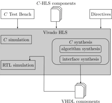
translated to a hardware implementation. Indeed, we design image de-compression algo-rithms using the actor oriented language under the RVC standard. Once the design is achieved, we use a dataflow compilation infrastructure calledOrccto generate a C-based code. Afterward, a Xilinx HLStool called Vivado is used for an automatic generation of synthesizable hardware implementation.
• Then, we propose a new interface synthesis method that enables the enhancement of the
implementation of the communication channels between components and therefore the en-hancement of scheduling policies, aiming at optimizing performance metrics such as latency and throughput of dataflow-based video decoders. Therefore, a new system level imple-mentation is elaborated based on this optimized impleimple-mentation of the communication and scheduling mechanisms.
• Next, we investigate techniques as an aid for DSEfor achieving high performance imple-mentations by exploiting task or data-level parallelism at the system-level.
• Finally, we present a framework for system or component-level verification. Hence, we
have demonstrated the effectiveness of our proposed rapid prototyping by applying it to anRVC-CAL implementation of theHEVCdecoder, which is very challenging because it typically involves high computational complexity and massive amounts of data processing.
1.3
Outline
This thesis is structured as follows.
PartI outlines the background to the study including its theoretical framework. Following the thesis’s introduction, Chapter2 entails an overview of trends and challenges in embedded sys-tems design and the emergence of system-level design of embedded syssys-tems. Chapter3reviews basic properties of the dataflow programming, introduces theMPEG-RVCframework as well as its reference programming language and the semantics of theDPNmodel. Then, it summarizes the existingHDLcode generation approaches from dataflow representations.
PartIIpresents the major contributions of this thesis. In Chapter4, a rapid prototyping method-ology for DPN-based programs is presented. The proposed design flow combines a dataflow compiler for generating C-basedHLSdescriptions from a dataflow description and a C-to-gate synthesizer for generating RTL descriptions. The results obtained applying to an RVC-CAL HEVC decoder are discussed. Chapter 5 presents optimization techniques by proposing new interface synthesis method firstly and further by exploiting all the features of dynamic dataflow. Chapter6 concludes the two parts of this thesis and discusses directions for future work. Part IIIprovides supplementary information to this thesis. In Appendix A, we present a user guide to the hardware generation from dataflow programs using our proposed design flow. Ap-pendices Band C present all available HEVC test sequences and a summary of Vivado HLS directives, respectively. Finally, AppendixDprovides a brief explanation of the work presented in this thesis in French.
1.4
Publications
The work presented in this thesis is partly published in the following publications. International Journal paper
M. Abid, K. Jerbi, M. Raulet, O. Deforges, and M. Abid. Efficient system-level hardware synthesis of dataflow programs using shared memory based FIFO: HEVC decoder case study. submitted to the Journal of Signal Processing Systems (under review), 2015.
International Conference paper
M. Abid, K. Jerbi, M. Raulet, O. Deforges, and M. Abid. System level synthesis of dataflow programs: HEVC decoder case study. In Electronic System Level Synthesis Conference
Part I
BACKGROUND
2
Fundamentals of Embedded Systems Design
“
Basic research is what I’m doing when I don’t know what I’m doing.”
Wernher von Braun
2.1
Introduction
In this chapter, I will look at the emergence of system-level design of embedded systems whose functionality involves real-time processing of media streams [Neuendorffer and Vissers, 2008], e.g., streams containing video data. In order to justify the needs of system-level design and the driving force behind its emergence, I must first set the stage for my study of embedded systems design and highlight challenges and complexities involved in designing embedded systems in Section 3.2. In section 2.3, I will give an overview of existing design methodologies linked to various levels of abstraction at which design process can be approached. Moreover, a taxonomy of design automation is developed by using the Y-chart [Gajski and Kuhn,1983] as a reference point. Section2.4and section2.5review the traditional design flows for embedded system design, including a discussion of their limitations. Section2.6presents motivating trends towards using system-level design.
2.2
The Embedded Systems Design
This section discusses some general aspects of embedded system design and highlights challenges and complexities involved in designing embedded systems.
2.2.1
What is an embedded system?
Embedded systems are defined as information processing systems embedded into enclosing prod-ucts such as cars, telecommunication or fabrication equipment. Such systems come with a large number of common characteristics, including real-time constraints, and dependability as well as efficiency requirements [Marwedel,2006]. A particular class of embedded systems are real-time systems. A real-time system is one in which the response to an event must occur within a specific time, otherwise the system is considered to have failed [Dougherty and Laplante, 1995]. The importance of embedded systems is growing continuously. That is, the evolution of embedded systems parallels Moore’s Law [Moore, 1965] which states that the number of transistors on Integrated Circuits (ICs) doubles approximately every two years. This IC technology advance enabled the design of embedded systems on a single chip called System On Chip (SOC). A
2.2. THE EMBEDDED SYSTEMS DESIGN 8
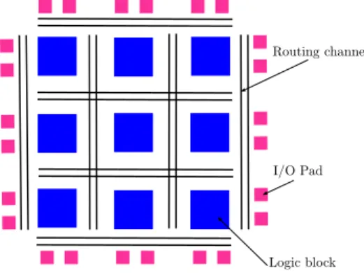
Routing channel
I/O Pad
Logic block
Figure 2.1: The basic FPGAstructure: a logic block consists of a 4-inputLUT, and aFF.
SOCis defined as a device which is designed and fabricated for a specific purpose, for exclusive use by a specific owner [Amos et al., 2011]. In other words, a SOC is a single piece of silicon that contains all circuits required to deliver a set of functions. It may include on-chip mem-ory, embedded processor, peripheral interfaces, and other components necessary to achieve the intended function. It may comprise more than one processor core, referred to as multiproces-sor System On Chip (MPSoC), where each of the embedded core whill take care of different sub-functions. SOCs can be implemented as Application-Specific Integrated Circuits (ASICs) or using Field-Programmable Gate Arrays (FPGAs).
2.2.1.1 What is an ASIC?
AnASICis a unique type ofICmeant for a specific application. Developing anASICtakes very much time and is expensive. Furthermore, it is not possible to correct errors after fabrication.
2.2.1.2 What is aFPGA?
An FPGA is a reprogrammable IC, i.e it can be programmed for different algorithms after fabrication. FPGAaddresses the cost issues inherent inASICfabrication.
FPGAarchitecture 1The basic structure of anFPGAis composed of the following elements: • Look-up table (LUT): this element performs logic operations.
• Flip-Flop (FF): this register element stores the result of theLUT.
• Wires: these elements connect resources to one another.
• Input/Output (I/O) pads: these physically available ports get data in and out of the
FPGA.
The combination of these elements results in the basic FPGA architecture shown in Figure 2.1. TheFPGAfabric includes embedded memory elements that can be used as Random-Access Memory (RAM), Read-Only Memory (ROM), or shift registers. These elements are block RAMs (BRAMs),LUTs, and shift registers.
• The BRAM is a dual-port RAM module instantiated into the FPGA fabric to provide on-chip storage for a relatively large set of data. The two types of BRAM memories available in a device can hold either 18 k or 36 k bits. The number of these memories available is device specific. The dual-port nature of these memories allows for parallel, same-clock-cycle access to different locations.
• The LUT is a small memory in which the contents of a truth table are written during device configuration.
• The shift register is a chain of registers connected to each other. The purpose of this
structure is to provide data reuse along a computational path.
2.2. THE EMBEDDED SYSTEMS DESIGN 9 Transform/ Scale/Quant Scaling and inverse transform i Motion Compensation Motion Estimation Entropy Encoding + + video input compressed Bitstream output
Mot ion dat a Quant ized coefficient s i + + video input compressed Bitstream output
Mot ion dat a Quant ized coefficient s
Figure 2.2: Hybrid video encoder [Jacobs and Probell, 2007].
CommercialFPGAdevices Since the release of the first Xilinx XC2064 commercialFPGA in 1985, the market ofFPGAs has been steadily growing. Xilinx and Altera are the two main FPGA manufacturers. The latest FPGAs are Xilinx Virtex-7 and Altera Stratix-V which are targeting highest performance and capacity. For instance, Virtex-7FPGAdelivers up to 2 million programmable logic cells (LUTs) and offer more than 4Tbps of serial bandwidth.
FPGA parallelism Unlike processors, FPGAs are inherently parallel, so that different pro-cessing operations do not have to compete for the same resources. Each independent propro-cessing task is assigned to a specific section of the circuit, and can run independently without depending on any other logic blocks. As a result, the performance of one part of the application is not affected when additional processing is added. The parallel computing power of FPGA is well suited for algorithms requiring high bandwidth and for the calculation of many operations in parallel on video data such as real-time video processing algorithms.
2.2.2
Video compression in
FPGA
For a video processing perspective, read-time can mean that the total processing per pixel must be completed within a pixel sample time [Bailey, 2011]. Real-time video processing need in embedded systems arises for video telephony, digital cameras, digital television, high definition TV decoders, DVD players, video conferencing, internet video streaming and other systems. All video storage and transmission mechanisms rely heavily on video compression and decompres-sion systems (known as CODECs). To enable interoperability, most products use standards-based digital video compression techniques. Video coding standards have evolved through the development of the International Standardization Organization/International Electrotechnical Commission (ISO/IEC) and International Telecommunication Union–Telecommunication sector
(ITU–T) standards. TheISO/IECMoving Picture Experts Group (MPEG)–1 [ISO/IEC
11172-2:1993],MPEG–4 Visual [ISO/IEC 14496-2:1999], and theITU–TH.261 [ITU-T Rec. ,12/90], H.263 [ITU-T Rec. H.263 , 03/96] are some of the popular international video compression standards. The essential underlying technology in each of these video compression standards is very similar and uses a hybrid video coding scheme (i.e., motion compensation, transform, quantization, entropy coding) as illustrated in Figure 2.2. The standards differ in the applica-tions they address. Each standard is tuned to perform optimally for a particular application in terms of bit rates and computational requirements: MPEG–1 for CD–ROM, MPEG–4 Visual for Television and Web environments, H.261 for videoconferencing, and H.263 for videophones. The H.264/MPEG–4 Advanced Video Coding (AVC) [ITU-T Rec. H.264 and ISO/IEC 14496-10], jointly developed by ITU–TVideo Coding Experts Group (VCEG) and ISO/IEC MPEG, provides up to 50% more bit rate reduction at the same quality of other existing standards. As a result of this significant advancement in compression technology, H.264/MPEG–4AVCis used in a wide variety of applications. The growing popularity of High Definition (HD) video, and the emergence of beyond HD formats (e.g., 4k × 2k or 8k × 4k resolution) are creating even stronger needs for coding efficiency superior to H.264/MPEG–4 AVC’s capabilities. Need for a codec superior than H.264/MPEG–4 AVC was result in the newest video coding stan-dard High-Efficiency Video Coding (HEVC) [Bross et al., 2012], which was finalized in 2013. HEVC is based on the same structure as prior hybrid video codecs like H.264/MPEG–4 AVC
2.2. THE EMBEDDED SYSTEMS DESIGN 10
but with enhancements in each coding stage. The goal ofHEVCis to increase the compression efficiency by 50% as compared to that of the H.264/MPEG–4AVC. The higher compression rate achieved in HEVC results in an increase in computational complexity for video encoding and decoding. HEVCencoders are expected to be several times more complex than H.264/MPEG– 4 AVC encoders [Bossen et al., 2012]. There is also a slightly increase in the computational complexity of video decoder. Due to the high computational complexity involved and to the huge amount of data that needs to be processed, high processing power is required to satisfy the real-time constraints. This can be more readily achieved through hardware parallelism. Intuitively, reconfigurable hardware in the form of FPGA has been proposed as a way of ob-taining high performance for video processing algorithms, even under real-time requirements. Moreover, implementing video processing algorithms on reconfigurable hardware minimizes the time-to-market cost, enables rapid prototyping of complex algorithms and simplifies debugging and verification. Therefore, FPGAs are an ideal choice for implementation of real-time video processing algorithms.
2.2.3
The embedded systems design challenges
Systems design is the process of deriving, from requirements, a model from which a system can be generated more or less automatically. A model is an abstract representation of a system. For example, software design is the process of deriving a program that can be compiled; hardware design is the process of deriving a hardware description from which a circuit can be synthesized [Henzinger and Sifakis,2006]. So, why is it so hard to design the real-time embedded system? The design of embedded systems is a challenging issue, for the following reasons:
2.2.3.1 Design constraints
1. Real-time constraints: embedded systems have to perform in real-time. If data is not ready by a certain deadline, the system fails to perform correctly. Real-time constraints are hard, if their violation causes the failure of the system functioning, and soft, otherwise. In the field of embedded video compression systems, there are latency and throughput constraints. The latency constraints states that the interval between the time Tavail, when the input data are available to the system, and Tprod, when the corresponding output data are produced must be less than the constraint ∆T .
Tprod− Tavail ≤ ∆T (2.1)
The throughput constraint states that the interval between the time Tstarting, when data processing is starting, and Tending, when data processing is finished must be less than ∆T .
Tending− Tstarting ≤ ∆T (2.2)
2. Small size and weight : typically, embedded systems are physically located within some larger device. Therefore, their shape and size may be dictated by the space available and the connections to the mechanical components.
3. Low Power and low energy consumption: in mobile applications, embedded designs are powered by batteries. This requires designs with low energy consumption. Power con-sumption is important also in applications in which the large amounts of heat produced during the circuit operation are difficult to be dispersed.
4. High-Performance: an embedded system should perform its functions and complete them quickly and accurately.
5. Reliability constraints: embedded systems are often used in life critical applications that is why reliability and safety are major requirements.
6. Low cost : embedded systems are very often mass products in highly competitive markets and have to be shipped at a low manufacturing and design cost.
7. Short time-to-market : time-to-market is the length of time from the product idea concep-tion until it is available for sale.
2.3. HARDWARE DESIGN METHODOLOGIES 11
Figure 2.3: Difference between design complexity and design productivity: the productivity gap. Source: Sematech2
Embedded Video Codec Design Requirements and Constraints The key challenge for embedded system design is how to implement a system that fulfills a desired functionality (e.g., video compression functionality) and simultaneously optimize the aforementioned design metrics in a timely fashion. First, during design of such real-time embedded systems, ensuring temporal correctness of their behavior is equally important as ensuring its functional correctness. Second, the need to execute complex video processing algorithms under tight timing constraints implies that the embedded systems have to be designed to sustain the ever-increasing computational complexity and to be extremely high performance. Third, to be suitable for the deployment in the consumer electronics products described in Section2.2.2, these embedded systems must be optimized to have low cost and low power/energy consumption.
2.2.3.2 Design productivity gap
The Semiconductor Industry Association (SIA)2 shows that a design productivity gap exists
between the available chip capacity and the current design capabilities. Figure2.3plots Moore’s Law, together with the productivity growth, expressed in transistors per staff member per month over the last decades. Due to improving engineering skills, an increase in the number of transis-tors that one designer can handle can be observed. The pace at which the design productivity increases is, however, much smaller than the slope of Moore’s Low. That is, whereas Moore’s Low predicts that the chip capacity doubles every eighteen months, the hardware design produc-tivity in the past few years is estimated to increase at 1.6× over the same period of time. As can be seen from Figure2.3, the design productivity gap originate from the 1980s. At that moment, it became clear that it was no longer possible in digital design to cope with every transistor indi-vidually. This ”design crisis” was the driven force behind the introduction of design abstraction levels [Bell and Newell,1971] together with well-defined design methodologies and the advent of the automation of the design of electronic systems and circuits (Electronic Design Automation (EDA)) [Lavagno et al.,2006]. Hence, design methodologies become a popular research topic to tackle these aforementioned design challenges of embedded systems in the recent decade.
2.3
Hardware Design Methodologies
In order to explain the different design methodologies, I will use the Y-Chart, which was intro-duced in 1983 by Gajski and Kuhn [Gajski and Kuhn,1983] and refined by Walker and Thomas [Walker and Thomas,1985]. The Gajski-Kuhn Y-chart is depicted in Figure2.4(a). This model
of design representation is described using three axes, each representing one of three domains of
description-behavioral, structural, and physical. The behavioral domain describes the behavior, or functionality, of the design, ideally without any reference to the way this behavior is achieved by an implementation. The structural domain describes the abstract implementation, or logical structure, of the design as a hierarchy of components and their interconnections. The physical domain describes the physical implementation of the design.
2Sematech Inc. International Technology Roadmap for Semiconductors (ITRS), 2004 update, design. http://
2.3. HARDWARE DESIGN METHODOLOGIES 12 SystemAlgo RTL LogicCircuit Physical Structural Behavioral
(a) Levels of abstraction versus do-mains of description. Physical Structural Behavioral synthesis analysis optimization generation extraction refin em ent ab strac tion (b) Y-tasks.
Figure 2.4: Gajski-Kuhn Y-chart.
2.3.1
Levels of abstraction
The concentric circles of the Y-chart represent the different levels of abstraction (Figure2.4(a)). The level of detail increases from the outside inward.
• System-level: defining the partitions of the system (as processes) and the communication
methods and interfaces between the partitions and the outside world. The system-level is concerned with overall system structure and information flow.
• Algorithmic-level, behavioral-level or high-level: behavioral modeling with high-level
pro-gramming languages of the computation performed by an individual process, i.e., the way it maps sequences of inputs to sequences of outputs.
• Register-Transfer Level (RTL): describing the circuit in terms of registers and the data transfers between them using logical operations (combinational logic).
• Logic-level or gate-level: defining the behavior of RTLcomponents with a set of intercon-nected logic gates and flip-flops.
• Circuit-level or transistor-level: implementing the behavior of the logic gates with
inter-connected transistors.
The main components that can be found at the different levels of abstraction are represented graphically in Figure2.5. As an example, consider a binary counter. At the algorithmic-level, we know that the counter increments its current value, producing a new value. At the next lower level, we understand that to carry out this function, some sort of register is needed to hold the value of the counter. We can state this idea using a register transfer statement such as AC ← AC + 1. On the structural side, the register consists of gates and flip-flops, which themselves consist of transistors [Null and Lobur,2010].
The Y-chart provides also a convenient framework for the definition of design tasks. They can be expressed as transitions between points on the axes of the chart as illustrated in Figure
2.4(b). Based on these transitions, the terms generation, extraction, synthesis and analysis can
be defined. Transitions from the structural domain to the physical domain are called generation, reverse transitions are are called extraction, those from the behavioral to the structural domain are called synthesis, and transitions in the opposite direction are called analysis. The task of synthesis is to take the specifications of the behavior required for a system and a set of constraints and goals to be satisfied and to find a structure that implements the behavior while satisfying the goals and constraints [Mohanty et al., 2008]. The tasks of refinement and optimization can be demonstrated on the Y-Chart as well. Refinement is represented by an arrow on the behavioral axis from a high to a lower abstraction level. On the other hand, optimization can be represented as an arrow at any point in the chart which points back to its starting point. Thus, such optimization is a task that is performed in-place and can occur at any level in any domain. In optimization, the basic functionality remains constant, but the quality of the design (in terms of performance, area and power consumption for example) is improved.
2.3. HARDWARE DESIGN METHODOLOGIES 13
(a) The main components at different abstrac-tions levels in the Y-chart [Michel et al.,2012].
(b) Graphical representation of the main components at different levels of abstraction [Verhelst and Dehaene,2009].
Figure 2.5: Different representations of the main components at each abstraction level.
circles in the Y-chart. We will explain in the following some basic system design methodologies related to the different abstraction levels in the Y-chart [Gajski et al.,2009].
2.3.2
Bottom-up methodology
The bottom-up design methodology starts from the lowest abstraction level, and each level generates libraries for the next-higher abstraction level as highlighted in Figure 2.6(a). The advantage of this methodology is that abstraction levels are clearly separated, each with its own library. The disadvantage is that optimal library for a specific design is difficult to achieve since parameters need to be tuned for all the library components at each level.
2.3.3
Top-down methodology
In contrast to bottom-up methodology, the top-down methodology starts with the highest ab-straction level to convert from functional description of the system into system structure as highlighted in Figure 2.6(b). The advantage of this approach is that high-level customization is relatively easy without implementation details, and only a specific set of transistors and one layout is needed for the whole process. The disadvantage is that it is difficult to get the accurate performance metrics at the high abstraction levels without the layout information.
2.3.4
System design process
The Y-chart separation of concerns, i.e. separating application (behavior) from architecture (structure) [Kienhuis et al., 1997], leads to the following five-step approach in the embedded system design process which I detail in the following. In a top-down way, a design always starts from system-level specifications and ends with a physical implementation of the system as depicted in Figure2.7. The bottom-up process works in reverse.
1. The requirements are the customer’s expectations about what the system has to achieve. A system specification includes not only functional requirements-the operations to be
per-2.3. HARDWARE DESIGN METHODOLOGIES 14
Physical
Structural Behavioral
start
(a) The bottom-up methodology.
Physical
Structural Behavioral
Start
(b) The top-down methodology. Figure 2.6: Design methodologies in the Y-chart.
System integration Components Architecture Specification Requirements Bottom-up design Top-down design
Figure 2.7: Major steps in the embedded systems design process [Wolf,2008].
formed by the system but also nonfunctional requirements, including speed, power, and manufacturing cost as explained in Section 2.2.3.1.
2. The specification states only what the system does, not how the system does things. Once the specification is determined, the design process involving various levels of abstraction is performed.
3. The architecture gives the system structure in terms of large components.
4. The architectural description tells us what components we need. The component design effort builds those components in conformance to the architecture and specification. 5. After the components are built, the system integration puts together the components to
build a complete system.
For the rest of the manuscript, I focus on the top-down design methodology that transform a given high-level system description into a detailed implementation.
2.3.5
Design flow and taxonomy of synthesis
The Y-chart also serves as a model of design synthesis using the multiple levels of abstraction and the three domains of description. Design synthesis is a path through the Gajski-Kuhn Y-chart from a high-level (of abstraction) behavioral domain description to a low-level physical domain description. This design flow includes translating and building inter-domain links from the behavioral to the structural to the physical domain, as well as adding enough additional detail to produce a low-level description from a high-level one. Thus the end goal of design synthesis (or design flow) is to produce a physical domain description at a low enough level to be implemented in hardware [Walker and Thomas, 1985]. Many alternative flows through
2.4. RTLDESIGN 15
Figure 2.8: The evolution of design methodology adoption in theEDA industry3.
the Y-chart are possible. We distinguish between transistor-level design, logic-level design,RTL design, high-level design, and system-level design corresponding to the input on circuit-level, logic-level,RTL, algorithmic-level and system-level, respectively.
We expand on all these design flows in the sections that follow, tracing thereby theEDAhistory [Sangiovanni-Vincentelli,2003] and the evolution of the design flow over the last decades [Jansen, 2003], aiming at increasing design productivity.
2.4
RTL
Design
As shown in Figure 2.8, raising the level of abstraction is one of the major contributors to the design productivity improvement. This chart shows the evolution of IC design from the mid-1970s to the present. There were gradual advancements to the IC technology through Small Scale Integration (SSI), Medium Scale Integration (MSI), Large Scale Integration (LSI), Very Large Scale Integration (VLSI) technology that evolved in the 1970s and the most recent is Ultra Large Scale Integration (ULSI) technology:
• SSI: contains less than ten logic gates perIC;
• MSI: contains ten to hundred logic gates perIC;
• LSI: contains hundred to ten thousand logic gates per IC;
• VLSI: contains more than ten thousand of logic gates perIC;
• ULSI: contains hundreds of thousands of logic gates perIC.
Since ICs were designed, optimized, and laid out by hand until the late 1960s, new Computer Aided Design (CAD) tools appeared to automate the design process from the 1970s.
From the mid-1970s to the early 1980s, the first incarnation of design synthesis operated at the transistor-level, and is called transistor-level design. At this level, designers used procedural languages to construct and assemble parameterized building blocks. The basic building blocks are transistors, resistors, capacitors, etc. The transistor-level design flow is shown in Figure
2.9(a). The behavioral description is done by a set of differential equations, whereas the
phys-ical description of the transistor-level comprises the detailed layout of components and their interconnections. Simulation Program for Integrated Circuit Emphasis (SPICE) is used for the transistor-level simulation to verify whether the logic design specified at the transistor-level will behave the same as the functional specifications. Although SPICEsimulation dramatically im-proved designer productivity of ICs through the 1970s, they are merely verification tools and design automation tools which are needed to speed up the design process and keep up with Moore’s Law.


![Figure 3.2: The first dataflow representation as introduced by Sutherland in 1966 [Sutherland, 1966].](https://thumb-eu.123doks.com/thumbv2/123doknet/14493838.718039/57.892.174.667.242.463/figure-first-dataflow-representation-introduced-sutherland-sutherland.webp)
![Figure 3.5: The conceptual process of deriving a decoding solution by means of normative and nonnormative tools in the RVC framework [Mattavelli et al., 2010].](https://thumb-eu.123doks.com/thumbv2/123doknet/14493838.718039/60.892.209.741.108.457/conceptual-deriving-decoding-solution-normative-nonnormative-framework-mattavelli.webp)
![Figure 3.7: Pictorial representation of the RVC-CAL dataflow programming model [Amer et al., 2009]](https://thumb-eu.123doks.com/thumbv2/123doknet/14493838.718039/63.892.231.606.110.376/figure-pictorial-representation-rvc-dataflow-programming-model-amer.webp)