HAL Id: hal-02263527
https://hal-amu.archives-ouvertes.fr/hal-02263527
Submitted on 10 Nov 2020HAL is a multi-disciplinary open access archive for the deposit and dissemination of sci-entific research documents, whether they are pub-lished or not. The documents may come from teaching and research institutions in France or abroad, or from public or private research centers.
L’archive ouverte pluridisciplinaire HAL, est destinée au dépôt et à la diffusion de documents scientifiques de niveau recherche, publiés ou non, émanant des établissements d’enseignement et de recherche français ou étrangers, des laboratoires publics ou privés.
Modeling and Simulation of SEU in Bulk Si and Ge
SRAM
Soilihi Moindjie, Daniela Munteanu, Jean-Luc Autran
To cite this version:
Soilihi Moindjie, Daniela Munteanu, Jean-Luc Autran. Modeling and Simulation of SEU in Bulk Si and Ge SRAM. Microelectronics Reliability, Elsevier, 2019, 100-101, pp.113390. �10.1016/j.microrel.2019.06.082�. �hal-02263527�
1
Modeling and Simulation of SEU in Bulk Si and Ge SRAM
S. Moindjie
a, D. Munteanu
a, J.L. Autran
a,*
a Aix-Marseille University & CNRS, IM2NP (UMR 7334), Faculté des Sciences – Service 142,
Avenue Escadrille Normandie Niémen, F-13397 Marseille Cedex 20, France
Abstract
In this work, the random-walk drift-diffusion (RWDD) model has been coupled to a circuit simulator to investigate single event upsets (SEU) induced by alpha particles in SRAM cells with silicon or germanium as bulk material. The impact of semiconductor charge generation and transport properties on the SEU mechanisms is quantified and discussed in a first-order approach considering ideal materials and generic devices. Our results suggest that the radiation response of Ge-based SRAM should be similar to the one observed for Si-SRAM, the benefits of higher mobilities at circuit level for germanium offsetting the negative impact of a relatively low energy value for electron-pair creation on transient current pulse magnitudes.
Keywords
Germanium, silicon, SRAM, single event upset (SEU), alpha particle, random-walk drift-diffusion, radiation transport, circuit simulator
Highlights
• The radiation responses of germanium and silicon-based SRAM cells have been compared • Numerical simulations investigate the occurrence of single event upsets induced by alpha particles • The impact of semiconductor properties in terms of charge generation and transport has been analyzed • This study gives a first-order indications on the susceptibility of germanium-based SRAM to radiation •
* Corresponding author:
Prof. Jean-Luc Autran, IM2NP - UMR CNRS 7334, Faculté des Sciences – Service 142, Avenue Escadrille Normandie – F-13397 Marseille Cedex 20 France – Phone: + 33 (0)413 594 627 – Email: [email protected]
2
1. Introduction
There is a growing interest in high-mobility channel materials for pushing the CMOS downscaling beyond the current silicon limit. Since the integration of high-permittivity materials as an alternative to thermal gate oxides, germanium (Ge) CMOS is considered as a promising alternative to Si because the bulk mobility values of electrons and holes in Ge are much higher than those of electrons and holes in Si (see Table 1) [1-4]. From a radiation response point-of-view, the question of the susceptibility of Ge to natural radiation, primarily atmospheric neutrons, has been recently investigated [5]. On one hand, with a number of interactions close to the one observed in silicon for identical target geometries [5], Ge therefore presents a lower energy for electron-pair creation than Si due to its lower bandgap, 2.9 eV versus 3.6 eV respectively [6]. This difference has a direct negative impact on the magnitude of single event transients created by the passage of ionizing particles in the semiconductor [7] because it signifies that, for a given LET particle, the deposited charge will be +24% larger in Ge than in Si. On the other hand, with an Ion current expected to be larger in both n-channel and p-channel Ge MOS transistors with
respect to Si devices of identical geometries, this theoretical gain in current will give a certain robustness advantage for Ge SRAM stability with respect to the one of Si SRAM. The aim of this work is precisely to explore this dual aspect of Ge SRAM subjected to the direct impact of ionizing particles (alpha particles in this study) in the sensitive drain of the memory cell and to compare it to the reference silicon case. Due to the current lack of experimental data concerning SEUs in bulk germanium SRAM, this study can be considered as a first tentative to investigate via numerical simulation the susceptibility to radiation of Ge SRAM in the ideal case of pure materials with no defects, no limiting mechanisms (potentially impacting carrier mobility and lifetime) and generic bulk MOS devices.
The paper is organized in two main sections: section 2 details our simulation approach for both radiation transport and electrical circuit solving; section 3 presents and discuss our simulation results for both Si and Ge cases in terms of transient current pulse characteristics and SEU occurrence in a standard SRAM cell designed in CMOS bulk 180nm.
3
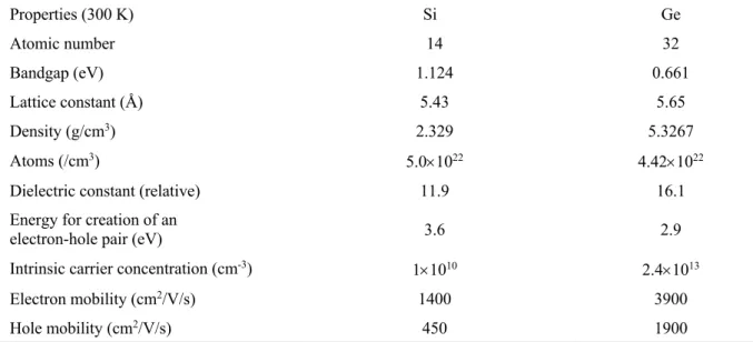
Properties (300 K) Si Ge Atomic number 14 32 Bandgap (eV) 1.124 0.661 Lattice constant (Å) 5.43 5.65 Density (g/cm3) 2.329 5.3267 Atoms (/cm3) 5.0´1022 4.42´1022Dielectric constant (relative) 11.9 16.1
Energy for creation of an
electron-hole pair (eV) 3.6 2.9
Intrinsic carrier concentration (cm-3) 1´1010 2.4´1013
Electron mobility (cm2/V/s) 1400 3900
Hole mobility (cm2/V/s) 450 1900
Table 1. Main properties for silicon and germanium at 300 K.
2. Modelling approach and numerical details
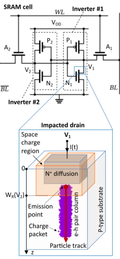
Figure 1 illustrates the methodology developed in this work. We considered a standard SRAM cell composed of six MOSFETs. Four transistors (N1, N2, P1, P2) form the storage cell (two cross-coupled inverters #1 and #2)
that has two stable states used to represent the “0” and “1”. Two additional access transistors (A1, A2) serve to
control the access to the storage cell during read and write operations. The transient radiation response and stability of this cell is studied in retention mode (blocked transistors A1 and A2) by simulating the passage of an ionizing
particle in the drain region of one of the off-state transistors (N1 in the example of Fig. 1). As shown in Fig. 1, the
impacted drain is modeled in the 3D space domain as a collection of rectangular boxes, representing the substrate, the drain diffusion and the back-end-of-line structure (stack of metal and insulating material layers, not shown). Because the 3D simulation domain is limited to the drain structure, it should be noted that simulation results will not depend on the SRAM layout. For the same reason and due to the direct nature of the impact in the drain, the notion of sensitive volume is not pertinent in the present approach.
The internal structure of the drain is an abrupt N+-P junction defined by the geometrical dimensions (W, L, h) of
the N+ diffusion contact, the doping levels of the two regions (NA, ND) and the bias potential (V1) applied to the
cathode. It must be noted that both the width (WSCR) and the maximum electric field (E) of this space charge region
depends, not only on the drain bias potential, but also on two semiconductor constants, i.e. the dielectric constant and the intrinsic carrier concentration (values given in Table 1 for Si and Ge). It results from this remark that WSCR
4
and E will have different values for Ge or Si drain junctions, also depending on the doping levels NA and ND; suchdifferences may influence the mechanisms of charge transport and collection, as discussed in the following (see section 3). To quantify this point in the case of an abrupt junction with typical doping levels NA = 1016 cm-3, ND =
1020 cm-3 and VR = 2 V, the following values are obtained : WSCR = 0.62 µm for Si and 0.67 µm for Ge (+8%) and,
in the same time, E = 9.47 MV/m for Si and 7.6 MV/m for Ge (-24.6%).
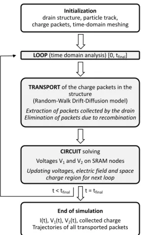
Fig. 2 shows the flowchart of the simulation code developed. After initialization of the structure (electrostatics of the drain junction) and computation of the charge packets along the particle track (as a function of the nature and energy of the incident particle using SRIM tabulated functions [8]), the simulation is performed in two steps: i) the transport of the radiation-induced charge within the drain structure using the random-walk drift-diffusion (RWDD) particle model [9] and ii) the SRAM circuit solving taking into account the radiation-induced parasitic current collected by the drain and injected into the circuit (at node V1 in the example of Fig. 1). These steps are
self-consistently solved over the whole time-domain from t=0 (impact of the particle) to t = tfinal (return to
equilibrium in the impacted zone). At the end of the simulation, transient current, collected charge and SRAM node voltages on the time domain are solved, as well as the “history” (trajectory, recombination or extraction) of each charge packets. Typical orders of magnitude for such numerical simulation are the following: 105 charge
packets, 250 time values ranging from 10-15 to 10-8 s with a geometrical progression, total simulation time of about
1 minute on quad-core workstation. Other details about equations and numerical implementations of both RWDD model and circuit solving can be found in [9-11].
5
Fig. 1. Methodology of simulation developed in this work.
V1 V2 VDD%% P2 N2 N1 P1 SRAM%cell Inverter%#1 Inverter%#2 I(t) P, typ e% su bs tr at e V1 Impacted%drain L 0 Par7cle%track Emission point N+%diffusion Space% charge% region z WR(V2) Charge% packet e,h%pa ir%c ol um n A2 A1
6
Fig. 2. Simplified flowchart of the simulation.
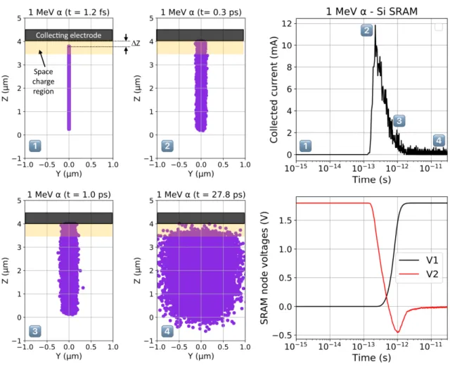
Fig. 3 illustrates such a simulation process in the particular case of a single event upset occurring in the SRAM (silicon case) due to the emission of a 1 MeV alpha particle in the middle of the space charge region of the transistor drain in the vertical direction oriented downwards. Charge packet distributions are represented at four different times, labeled #1 to #4, respectively corresponding to 1.2 fs, 0.3, 1.0 and 27.8 ps after the particle strike in the projected Y-Z plan of the 3D structure. These four pictures correspond to different values of the transient current, also labeled on the current curve. The result of this transient is the upset of the SRAM cell, evidenced by the changes in V1 (0®VDD) and V2 (VDD®0) values. Picture #1 shows the distribution of charge
packets immediately after the particle strike. These packets are distributed along the particle track with a linear density determined by SRIM; the transport of each packet starts, in parallel with the recombination process. At this time, no packet has reached the collecting electrode; consequently, the extracted current is null. Picture #2 corresponds to the extraction of the first charge packets located at the top of the track, in the space charge region where the electric field is high. The current increase and rapidly reaches a maximum. The track radius increases
Initialization drain structure, particle track, charge packets, time-domain meshing
LOOP (time domain analysis) [0, tfinal]
TRANSPORT of the charge packets in the structure
(Random-Walk Drift-Diffusion model)
Extraction of packets collected by the drain Elimination of packets due to recombination
CIRCUIT solving Voltages V1and V2on SRAM nodes
Updating voltages, electric field and space charge region for next loop
End of simulation I(t), V1(t), V2(t), collected charge
Trajectories of all transported packets t < tfinal t = tfinal
7
due to the diffusion mechanism. In pictures #3, extracted packets are less numerous than previously and current becomes limited by the diffusion mechanism in the neutral zone of the substrate (3D i.e. spherical diffusion) that feeds in packets the space charge region. Finally, picture #4 corresponds to the end of the transient pulse: long-term diffusion combined with carrier recombination dramatically decrease the quantity of packets susceptible to be collected and extracted from the drain electrode, the current tends to zero and the semiconductor progressively returns to equilibrium.Fig. 3. Cartoon of a single event upset occurring in the Si-SRAM due to the emission of a 1 MeV alpha particle in the space charge region of the transistor drain. Charge packet distributions are represented at t = 1.2 fs, 0.3, 1.0 and 27.8 ps after the particle strike in the projected Y-Z plan of the 3D structure.
8
3. Results and discussion
3.1. Transistors characteristics
0.18 µm n-channel and p-channel MOS transistor have been simulated considering the EKV v1.0 compact model of the drain current [12]. This model is perfectly continuous in all transistor operation regimes, captures the essential physics of the MOS transistor but does not consider the mobility dependence with the high electrical field and doping level and the band-to-band tunnelling. Threshold voltages of N-MOS and P-MOS have been adjusted in order to have the same off-current IOFF = 8´10-3 µA/µm at VG = 0V and VD = VDD. Due to higher electron and
holes mobilities, Ge transistors exhibit larger on-currents than for Si devices, respectively ION = 1170 µA/µm for P-MOS and ION = 2200 µA/µm for N-MOS, to be compared with ION = 253 µA/µm for
P-MOS and ION = 663 µA/µm for N-MOS in the case of Si. In absence of simulation calibration on experimental
data, these values remain theoretical and must be considered as an ideal and limit comparison case. Their interest in the following is to provide performance projections for Ge with respect to Si in the most favourable case, i.e. for the best transport properties theoretically reachable with a perfect material exempt of defects.
3.2. SRAM cell stability
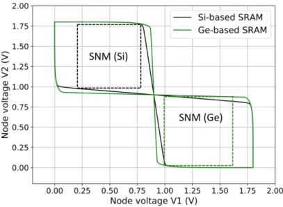
The stability and robustness of the designed SRAM cell designed has been investigated for both semiconductor materials, Si and Ge. Fig. 4 shows the corresponding butterfly curves that correspond to the voltage transfer characteristics of the two cross-coupled inverters #1 and #2 (see Fig. 1) in retention (hold) mode. From these curves, it is possible to extract the Static Noise Margin (SNM) that graphically corresponds to the diagonal of the largest square that fits within the back-to-back DC characteristics of the two inverters [13]. Results show that the SNM for the Ge-based SRAM is +11% higher than the SNM extracted for the Si-based SRAM. Such a result is logically due to the better on-currents obtained in the case of Ge-transistors with respect to Si-devices that contribute to increase the stability of the cell in retention mode, the other design parameters being the same for the two SRAMs.
9
Fig. 4. Butterfly curves for silicon and germanium-based SRAMs in retention (hold) operation and extraction of the retention SNM in both cases.
3.3. Critical charge determination
In order to confirm previous results, we performed a series of simulations to determine the critical charge of the SRAM cells. A low energy alpha particle was emitted in the middle of the space charge region of the drain contact in the horizontal direction, to ensure the collection of almost all the minority carriers (charge packets) created along the particle track. Fig. 5 shows the SRAM transient responses for different alpha initial energies. Both the initial time and durations of these transient responses are different for Si and Ge. For the critical energy values (red curves in Fig. 5), the Ge structure collects the charges in 2 ps whereas the transient regime ends after 10 ps for Si. As a result, Si-based SRAM is upset at 50.9 keV and Ge-based SRAM at 51.2 keV. Considering the e-h pair creation energies, respectively 3.6 eV for Si and 2.9 eV for Ge, these two values respectively correspond to an electrical charge equal to 2.26 fC for Si and 2.82 fC for Ge. These values are a good estimation of the critical charges for the two SRAM cells, confirming the greater robustness of the Ge cell with respect to the Si cell due to transistor better performances, primarily in terms of ION values.
10
Fig. 5. SRAM transient responses for low-energy alpha particles depositing all their energy in the drain space charge region.
3.4. SEU occurrence for alpha particles
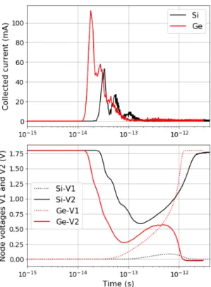
We examined the SEU occurrence for the particular case of alpha particles emitted in the drain structure in the vertical direction oriented downwards (as illustrated in Fig. 3) and also in the horizontal direction. The distance between the emission point and the drain electrode is noted DZ.
For alpha vertical tracks, we observed that SRAM cells are upset until a critical value of DZ, lower for Si than for Ge, which also depends on the energy (and consequently on the initial LET) of the particle. For example, for 1 MeV alpha, DZ are very short and inferior to the width of the space charge region: DZ = 0.05 µm for Si and DZ = 0.1 µm for Ge. Fig. 6 illustrates this case for precisely DZ = 0.1µm where SRAM in only upset for Ge. The large difference in charge deposition between Si and Ge, due to differences in the e-h pair creation energies, and the fast dynamics of charge collection explains such a behavior at low distances from the collecting electrode.
11
Fig. 6. SRAM transient responses for 1 MeV alpha particle emitted at DZ = 0.1 µm from the drain electrode in
the vertical direction oriented downwards.
In Fig. 6, note the formations of oscillations in the current transients due to the counter-reaction of the space charge region during the carrier collecting process. Indeed, the width of this space charge region depends on the voltage V2, which is varying due to the circuit reaction. This is a main difference with a simulation considering a fixed
drain voltage and, consequently, neglecting the effect of the rest of the circuit connected to the transistor drain. For horizontal alpha tracks, we also performed many simulations to explore the impact of DZ on the upset occurrence. Contrary to the previous case, when a particle deposits its energy completely outside the space charge region, the current becomes limited by the diffusion of carriers generated in the neutral zone. These carriers diffuse to the space charge region and are then rapidly collected by drifting under the action of the electric field. In this case, the other pertinent factor with respect to the collected charge is the minority carrier mobility, in addition to the e-h pair creation energy. For 1 MeV horizontal alphas, DZ is surprisingly found slightly larger for Si (DZ = 0.41 µm) than for Ge (DZ = 0.39 µm). It signifies that one can find DZ values (between these two limits) for which the Si-SRAM is upset and not the Ge-SRAM. This singular case is illustrated for DZ = 0.39 µm in Fig. 7. In this example, the intrinsic robustness of the Ge-SRAM circuit is enough to absorb a larger current pulse, contrary to
12
the case of the Si-SRAM, which is upset by a lower pulse.Fig. 7. SRAM transient responses for 1MeV alpha particle emitted at a distance DZ = 0.39 µm from the drain
electrode in the horizontal direction.
4. Conclusion
In conclusion, we successfully coupled the random-walk drift-diffusion (RWDD) model to a circuit simulator to investigate single event upsets (SEU) induced by alpha particles in SRAM cells with silicon or germanium as bulk material. This preliminary work evidenced and explored the dual aspect of germanium with respect to silicon from a radiation response point-of-view: i) its theoretical gain in carrier mobility that contributes to reinforce the robustness of circuit and ii) its lower energy for electron-pair creation that induces more electrical charges in the material for the same amount of deposited energy. We illustrated the impact of these two essential characteristics of germanium on the SEU response of a generic 0.18 µm SRAM cell subjected to alpha particles. At this level of our investigations and considering the different simplifications inherent to the present first-order modelling approach (direct impact in the drain structure, no dependence of the circuit layout, simplified drain structure, ideal materials and devices), these results suggest that the radiation response of Ge-based SRAM should be similar to
13
the one observed for Si-SRAM; in other words, the benefits of higher mobilities at circuit level offsetting the negative impact of a relatively low energy value for electron-pair creation on transient current pulse magnitudes. These results should be confirmed or infirmed on other particles at various lower and higher LET in future studies. The impact of the transistor modelling on the simulation results may be also carefully evaluated to apply, in future works, for realistic SRAMs with feature size down to nanometers.References
[1] Toriumi A, Nishimura T. Germanium CMOS potential from material and process perspectives: Be more positive about germanium. Japanese Journal of Applied Physics 57, 2018, pp. 010101.
[2] Saraswat KC, Chui CO, Kim D, Krishnamohan T, Pethe A. High Mobility Materials and Novel Device Structures for High Performance Nanoscale MOSFETs. IEDM Techn. Digest (2006) 1-4.
[3] SaraswatKC, Kim D, Krishnamohan T, Kuzum D, Okyay AK, Pethe A Yu HY. Germanium for High Performance MOSFETs and Optical Interconnects. ECS Transactions, 16 (10) (2008) 3-12.
[4] Moreau M, Munteanu D, Autran JL, Bellenger F, Mitard J, Houssa M, Investigation of capacitance–voltage characteristics in Ge /high-j MOS devices. J. Non-Cryst. Solids 355 (2009) 1171-1175.
[5] Munteanu D and Autran JL. Susceptibility of Group-IV and III-V Semiconductor-based Electronics to Atmospheric Neutrons Explored by Geant4 Numerical Simulations. In: S. Rao (Ed.) Numerical Simulations, Intech, Vienna, 2018, pp. 117-134.
[6] Fang J. et al. Understanding the Average Electron–Hole Pair-Creation Energy in Silicon and Germanium Based on Full-Band Monte Carlo Simulations. IEEE Transactions on Nuclear Science 66, 2019, pp. 444-451.
[7] Munteanu D, Autran JL. Modeling and simulation of single-event effects in digital devices and ICs. IEEE Trans. Nucl. Sci. 55 (4) (2008) 1854–1878.
[8] Martinie S, Saad-Saoud T, Moindjie S, Munteanu D, Autran JL. Behavioral modeling of SRIM tables for numerical simulation, Nuclear Instruments and Methods in Physics Research B: Beam Interactions with Materials and Atoms 322 (2014) 2-6.
[9] Autran JL, Munteanu D., Moindjie S, Saad Saoud T, Malherbe V, Gasiot G, Clerc S, Roche P. Charge Collection Physical Modeling for Soft Error Rate Computational Simulation in Digital Circuits. N. Sher Akbar, O. Anwar Beg. Modeling and Simulation in Engineering Sciences, Intech, 2016, pp. 115-137.
14
[10] Autran JL, Glorieux M, Munteanu D, Clerc S, Gasiot G, Roche P. Particle Monte Carlo modeling ofsingle-event transient current and charge collection in integrated circuits. Microelectronics Reliability 54, 2014, pp. 2278-2283.
[11] Glorieux M, Autran JL, Munteanu D, Clerc S, Gasiot G, Roche P. Random-Walk Drift-Diffusion Charge-Collection Model For Reverse-Biased junctions Embedded in Circuits. IEEE Trans. Nucl. Sci. 61 (2014) 3527-3534.
[12] Enz CC, Krummenacher F, Vittoz EA. An Analytical MOS Transistor Model Valid in All Regions of Operation and Dedicated to Low-Voltage and Low-Current Applications. Analog Integrated Circuits and Signal Processing 8 (1995) 83-114.