HAL Id: hal-02100246
https://hal-amu.archives-ouvertes.fr/hal-02100246
Submitted on 15 Apr 2019
HAL is a multi-disciplinary open access
archive for the deposit and dissemination of
sci-entific research documents, whether they are
pub-lished or not. The documents may come from
teaching and research institutions in France or
abroad, or from public or private research centers.
L’archive ouverte pluridisciplinaire HAL, est
destinée au dépôt et à la diffusion de documents
scientifiques de niveau recherche, publiés ou non,
émanant des établissements d’enseignement et de
recherche français ou étrangers, des laboratoires
publics ou privés.
3D Simulation of Heavy Ions-Induced
Single-Event-Transient Effects in Symmetrical
Dual-Material DG MOSFET
Daniela Munteanu, Jean-Luc Autran
To cite this version:
Daniela Munteanu, Jean-Luc Autran. 3D Simulation of Heavy Ions-Induced Single-Event-Transient
Effects in Symmetrical Dual-Material DG MOSFET. ESREF Conference, Oct 2015, Toulouse, France.
�hal-02100246�
3D Simulation of Heavy Ions-Induced Single-Event-Transient Effects
in Symmetrical Dual-Material DG MOSFET
D. Munteanu
a, J.L. Autran
a,*a Aix-Marseille Univ, CNRS, Univ Toulon, IM2NP (UMR 7334), Faculté des Sciences – Service 142,
Avenue Escadrille Normandie Niémen, F-13397 Marseille Cedex 20, France
Abstract
Dual-Material Gate Double-Gate (DMDG) structure is promising for future ultra-scaled devices thanks to its capability to reduce SCEs and HCEs. This is due to a step in the surface-potential profile which screens the source side of the channel from drain-potential variations and reduces the drain electric field. In this work, we investigate the DMDG sensitivity to single-event transients. The impact of dual gate materials on the bipolar gain is particularly addressed. We show that DMDG is naturally less radiation immune than usual single-material DG (SMSG) devices.
Corresponding author.
[email protected]
Tel: + 33 (0)413 594 627; Fax: +33 (0)491 288 531
3D Simulation of Heavy Ions-Induced Single-Event-Transient Effects
in Symmetrical Dual-Material DG MOSFET
D. Munteanu
a, J.L. Autran
a,** Corresponding author. [email protected] Tel: + 33 (0)413 594 627; Fax: +33 (0)491 288 531
1. Introduction
Double-Gate (DG) MOSFETs have received particular interest in the last decades due to its promising capabilities for nanometer scaling. Many theoretical and experimental studies have reported on the very good control of parasitic short channel effects (SCE) and ideal subthreshold slope of DG transistors [1]. These performances are namely due to the additional gate electrode which sensibly improves the electrostatic control of the channel and allows using intrinsic channel providing no parasitic doping fluctuation effects and increased carrier mobility.
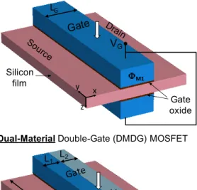
However, as the gate length shrinks, hot-carrier induced effects (HCE) and drain induced barrier lowering (DIBL) phenomena become important issues that need to be addressed [2, 3]. In order to prevent undesired HCEs and to enhance the immunity against SCEs, a new concept of DG MOSFETs with dual gate-material (DMDG) has been proposed and validated [4, 5, 6, 7]. Compared with the conventional single gate-material double-gate (SMDG) device (Fig. 1a), this new structure has two materials in the gates (Fig. 1b), M1 and M2 with different workfunctions, ΦM1 and
ΦM2, respectively. This configuration induces a step in
the surface-potential profile (see Fig. 2) which, for ΦM1>ΦM2, simultaneously provides transconductance
increase and DIBL reduction. The step function profile of the surface potential ensures screening of the channel region on the source side (under the material M1) from drain-potential variations. In addition, the peak electric field at the drain is considerably reduced, which suppresses HCEs [8].
The transient response of SMDG MOSFETs submitted to heavy-ion irradiation has been investigated by simulation in [9, 10]. These previous studies demonstrate that SMDG show better radiation hardness than fully-depleted Single-Gate SOI devices,
VG
Single-Material Double-Gate (SMDG) MOSFET
Dual-Material Double-Gate (DMDG) MOSFET
tSi W x y z Silicon film Gate oxide LG L1 L2 ΦM1ΦM2 VG ΦM1
Fig. 1. Schematic description of the simulated symmetrical SMDG and DMDG devices. For a better view, spacers and
isolation oxides are not shown.
particularly due to the enhanced control of the body potential and to the reduction of floating body effects. Concerning DMDG MOSFETs, extensive analytical modeling works have been reported in the literature [4, 5, 6, 7], but, at the best of our knowledge, radiation-sensitivity studies of these devices have not been performed. In this paper we investigate by 3-D numerical simulation the response to single-event of DMDG compared with that of SMDG. The impact of the material M2 workfunction on single-event transients and bipolar amplification is also addressed.
2. Simulated devices and models
Simulated SMDG and DMDG devices are designed with the same geometrical dimensions: channel length LG=20 nm, 100 nm gate width, 6
nm-thick intrinsic silicon film and 1 nm-nm-thick gate oxide, similar to real devices reported in [11]. In SMDG, a single-material M1 is used for the gates. In DMDG the gates consists of dual materials, M1 (ΦM1) and M2
(ΦM2), of lengths L1 and L2, respectively (L1+L2=LG).
In a first time we considered L1=L2=LG/2.
3-D numerical simulations have been performed with the DESSIS device simulator from Synopsis Inc. [12]. The main models used in simulation are the Shockley-Read-Hall and Auger recombination models, the Fermi-Dirac carrier statistics and the hydrodynamic model was used for the carrier transport equations. The impact ionization model depends on carriers energy. The mobility model includes the dependence on the carrier energy, lattice temperature and doping level.
The ion strike was simulated using the DESSIS HeavyIon module [12]. The electron-hole pair column created in the device by the ion strike is modeled using a carrier-generation function which has a Gaussian radial distribution with a characteristic radius of 20 nm, a Gaussian time distribution, centered on 10 ps and having a characteristic width of 2 ps. The ion strikes in the channel center (Fig. 1). Devices are biased in the off-state (VG=0V). The drain terminal is
constantly biased at the power supply voltage of 1 V.
3
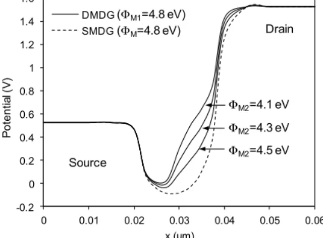
. Static characteristics of DMDG MOSFETsFigure 2 plots the surface potential profile in SMDG and DMDG for different ΦM2 values. This
figure shows, as expected, that the surface potential has
-0.2 0 0.2 0.4 0.6 0.8 1 1.2 1.4 1.6 0 0.01 0.02 0.03 0.04 0.05 0.06 Po te n tia l ( V) x (µm) DMDG SMDG (ΦM1=4.8 eV) (ΦM=4.8 eV) ΦM2=4.1 eV ΦM2=4.3 eV ΦM2=4.5 eV Source Drain
Fig. 2. Surface potential profile in SMDG and DMDG.
0 0.1 0.2 0.3 0.4 0.5 0.6 0.7 0.8 0 10 20 30 Dr ai n cu rr en t (µ A ) Time (ps) DMDG SMDG LET=0.1 MeV.cm2/mg (ΦM1=4.8 eV, ΦM2=4.1 eV) (ΦM=4.8 eV)
Fig. 3. Drain current transient in DMDG and SMDG MOSFETs for an ion hit in the channel center.
a step-function profile, responsible of DIBL reduction and transconductance enhancement in DMDG compared to SMDG.
4
. Heavy-Ion-Induced Transient: DMDG versus SMDG MOSFETs4.1. Drain current transient
Figure 3 shows the drain current transient resulting from an ion hit in the channel center of DMDG and SMDG for an ion with a linear energy transfer (LET) of 0.1 MeV.cm2/mg. The drain current transient peak is
higher and wider for DMDG than for SMDG device. The reason is probably a higher bipolar amplification in DMDG case (see next section) due to the step-function profile of the channel potential.
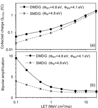
4.2. Collected charge and bipolar amplification
The variation of the collected charge, QCOLL, as
function of LET is plotted in Fig. 4a. QCOLL is obtained
by integrating the simulated drain current over the transient duration. The deposited charge, QDEP, is
calculated considering the Gaussian distribution of the ion track and the 3-D geometry of the silicon body. The bipolar gain is then given by the ratio between the QCOLL and QDEP. The bipolar amplification variations
in DMDG and SMDG are shown in Fig. 4b. The LET range considered here corresponds to the LET range of a neutron-induced ion in silicon in the terrestrial environment [13]. Figure 4 indicates that the bipolar amplification is higher in DMDG than in SMDG, particularly at low LET. The body potential modification in DMDG induced by the presence of a gate material with lower workfunction on the drain
0.01 0.1 1 0.1 1 10 Co lle ct ed c ha rg e QC OLL (f C ) LET (MeV.cm2/mg) DMDG SMDG (ΦM1=4.8 eV, ΦM2=4.1 eV) (ΦM=4.8 eV) 0 5 10 0.1 1 10 Bi p o la r a m p lif ic at io n LET (MeV.cm2/mg) DMDG SMDG (ΦM1=4.8 eV, ΦM2=4.1 eV) (ΦM=4.8 eV)
Fig. 4. Collected charge and bipolar amplification as function of LET in DMDG and SMDG MOSFETs for an
ion hit in the channel center.
side of the gate sensibly enhances the collected charge and the bipolar gain of the device compared to the SMDG counterpart. The difference between the two devices is important at low LET, but it gradually weakens when the LET value increases. The explanation is that at high LET the electric field is collapsed in both devices and then potential variations in the channel have less impact on the parasitic bipolar amplification. The bipolar gain then becomes nearly the same for DMDG and SMDG.
4.3. Ion hit location sensitivity
Previous simulations results have been obtained for an ion hit in the channel center (corresponding to x=30 nm). Since particles can strike the channel at different locations, we consider in the following several ion hit locations along the x-axis between the source contact (x=0) and the drain contact (x=60 nm). Drain current transients obtained for three locations in DMDG are shown in Fig. 5. The drain current peak and transient width increase as the ion strike location moves from source to drain. The collected charge as a function of the strike location in DMDG and SMDG is plotted in Fig. 6 for two different LET values. The deposited charge is also reported for comparison. QDEP
is highest in the middle of the channel and decreases toward the source and drain sides of the silicon film,
0 50 100 150 0 5 10 15 20 25 30 Dr ai n cu rr en t (µ A ) Time (ps) Source hit (x=10 nm) Channel center hit (x=30 nm) Channel-drain junction hit (x=40 nm) DMDG
Fig. 5. Drain current transients in DMDG MOSFETs for several ion hit locations (LET=10 MeV.cm2/mg).
0 0.02 0.04 0.06 0 10 20 30 40 50 60 Co lle ct ed c ha rg e QCO LL (f C )
Ion hit location (nm) DMDG SMDG LET=0.1 MeV.cm2/mg Deposited charge QDEP(fC) (ΦM1=4.8 eV, ΦM2=4.1 eV) (ΦM=4.8 eV)
0 0.2 0.4 0.6 0.8 1 1.2 0 10 20 30 40 50 60 Co lle ct ed c ha rg e QCO LL (f C )
Ion hit location (nm) DMDG SMDG LET=10 MeV.cm2/mg Deposited charge QDEP(fC) (ΦM1=4.8 eV, ΦM2=4.1 eV) (ΦM=4.8 eV)
Fig. 6. Collected charge in DMDG and SMDG MOSFETs as a function of the ion hit location.
because a reduced part of the ion track is contained in the active region [14]. QCOLL has a bell-shaped profile
with a maximum around the middle of the channel (where QDEP is the highest) and two minima at the
source and drain contacts (where QDEP is the lowest).
For all x locations QCOLL is lower in SMDG than in
DMDG. At very low LET=0.1 MeV.cm2/mg, QCOLL is
always higher than QDEP, which clearly indicates a
strong bipolar amplification (Fig. 7a). For ion strikes in the source and LET=10 MeV.cm2/mg QCOLL is lower
than QDEP. This indicates that the bipolar amplification
(Fig. 7b) is very low and that there is a strong recombination of the deposited charge in the device [14]. The bipolar gain (Fig. 7) is always higher in DMDG than in SMDG, but has similar dependences
(a)
(b) (a)
0 5 10 0 10 20 30 40 50 60 Bi p o la r a m p lif ic at io n
Ion hit location (nm) DMDG SMDG LET=0.1 MeV.cm2/mg (ΦM1=4.8 eV, ΦM2=4.1 eV) (ΦM=4.8 eV) 0 0.5 1 1.5 2 0 10 20 30 40 50 60 Bi p o la r a m p lif ic at io n
Ion hit location (nm) DMDG
SMDG
LET=10 MeV.cm2/mg
(ΦM1=4.8 eV, ΦM2=4.1 eV)
(ΦM=4.8 eV)
Fig. 7. Bipolar gain in DMDG and SMDG MOSFETs as a function of the ion hit location.
on ion hit location for both devices. For low LET, the bipolar gain maximum is located at the channel center and for high LET the highest gain is obtained at the channel-drain junction.
5
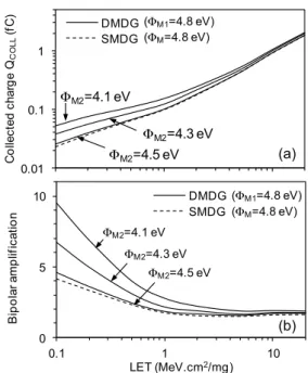
. Discussion: gate workfunction impact on single-event transient effects in DMDG MOSFETsWe also investigated the impact of several technological parameters on the transient response of DMDG. Simulations have been performed considering DMDG devices including a metal gate M2 with various workfunctions. At low LET, the simulation results indicate that the current transient peak and width, the collected charge and the bipolar gain monotonically decrease when ΦM2 is increased. This
decrease is strongly attenuated when ΦM2 becomes
higher than 4.5 eV, as shown in Fig. 8 for the collected charge and bipolar gain. At high LET, the transient response become sensibly the same for all devices (DMDG with different ΦM2 and SMDG), because, as
explained before, the high deposited charge collapse the electric field. Then the body-potential differences between the structures have a lesser influence on their transient response. For LET above about 5 MeV.cm2/mg the collected charge and the bipolar gain
become sensibly the same for all devices. Additional simulation results for different L1 and L2 values and
detailed discussion will be included in the full paper.
0.01 0.1 1 0.1 1 10 Co lle ct ed c ha rg e QC O LL (f C ) LET (MeV.cm2/mg) DMDG SMDG (ΦM1=4.8 eV) (ΦM=4.8 eV) ΦM2=4.1 eV ΦM2=4.3 eV ΦM2=4.5 eV 0 5 10 0.1 1 10 Bi p o la r a m p lif ic at io n LET (MeV.cm2/mg) DMDG SMDG (ΦM1=4.8 eV) (ΦM=4.8 eV) ΦM2=4.1 eV ΦM2=4.3 eV ΦM2=4.5 eV
Fig. 8. Collected charge and bipolar gain in DMDG and SMDG MOSFETs for an ion hit at x=40 nm.
References
[1]. J.T. Park and J.P. Colinge, IEEE Trans. Electron Devices, vol. 49, no. 12, pp. 2222–2229, Dec. 2002. [2]. D.J. Frank, S.E. Laux, M.V. Fischetti, Int. Electron
Devices Meeting Tech. Dig., pp. 553–556, 1992. [3]. H.-S.P. Wong, presented at the IEDM Short Course:
Sub-100 nm CMOS, Washington, DC, 1999. [4]. W. Long, H. Ou, J.-M. Kuo, K.K. Chin, IEEE Trans.
Electron Devices, vol. 46, no. 5, pp. 865–870, 1999. [5]. G.V. Reddy and M.J. Kumar, IEEE Trans.
Nanotechnol., vol. 4, pp. 260–268, Mar. 2005. [6]. M.J. Kumar and A. Chaudhry, IEEE Trans. Electron
Devices, vol. 15, no. 4, pp. 569–574, Apr. 2004. [7]. M. J. Kumar and G.V. Reddy, Jpn. J. Appl. Phys., vol.
44, no. 9A, pp. 6508–6509, Sep. 2005.
[8]. T.K. Chiang, Microelectronics Reliability, vol. 49, pp. 693-698, 2009.
[9]. D. Munteanu, V. Ferlet-Cavrois, J.L. Autran, P. Paillet, J. Baggio, O.Faynot, C. Jahan, and L. Tosti, IEEE Trans. Nucl. Sci., vol. 53, no. 6, p. 3363, 2006. [10]. D. Munteanu, J.L. Autran, V. Ferlet-Cavrois, P. Paillet,
J. Baggio, and K. Castellani, IEEE Trans. Nucl. Sci., vol. 54, no. 4, pp. 994–1001, 2007.
[11]. M. Vinet et al. IEEE Electron Dev. Lett., vol. 26, pp. 317-319, 2005.
[12]. Synopsys Sentaurus TCAD tools, Available online: http://www.synopsys.com/products/tcad/tcad.html. [13]. Y.P Fang and A.S. Oates, IEEE Trans. Device and
Material Reliability, vol. 11, pp. 551-554, 2011. [14]. D. Munteanu and J.L. Autran. Microelectronics
Reliability, vol. 54, pp. 2284-2288, 2014. (a)
(b)
(a)