HAL Id: hal-01324143
https://hal.archives-ouvertes.fr/hal-01324143
Submitted on 18 Dec 2018
HAL is a multi-disciplinary open access
archive for the deposit and dissemination of sci-entific research documents, whether they are pub-lished or not. The documents may come from teaching and research institutions in France or abroad, or from public or private research centers.
L’archive ouverte pluridisciplinaire HAL, est destinée au dépôt et à la diffusion de documents scientifiques de niveau recherche, publiés ou non, émanant des établissements d’enseignement et de recherche français ou étrangers, des laboratoires publics ou privés.
Piezoelectric tantalum pentoxide studied for optical
tunable applications
Rémy Parmentier, Fabien Lemarchand, Michel Cathelinaud, Michel Lequime,
Claude Amra, Stéphane Labat, S. Bozzo, Franck Bocquet, Ahmed Charaï,
Olivier Thomas, et al.
To cite this version:
Rémy Parmentier, Fabien Lemarchand, Michel Cathelinaud, Michel Lequime, Claude Amra, et al.. Piezoelectric tantalum pentoxide studied for optical tunable applications. Applied optics, Optical Society of America, 2002, 41 (16), pp.3270-3276. �10.1364/AO.41.003270�. �hal-01324143�
Piezoelectric tantalum pentoxide studied for
optical tunable applications
Re´my Parmentier, Fabien Lemarchand, Michel Cathelinaud, Michel Lequime, Claude Amra, Ste´phane Labat, Ste´phanie Bozzo, Franck Bocquet, Ahmed Charaı¨, Olivier Thomas, and Christian Dominici
Piezoelectric transparent thin films are of great interest for use in tunable filters. We present experi-mental results on Ta2O5 single layers
coated on fused-silica substrates with an electron-beam deposition process. Above 450 °C, coatings change from an amorphous to a polycrystallized structure. When this structure shows a preferred orientation matching the piezoelectric tensor of the Ta2O5 crystal and
the external electric field, variation in the piezoelectric layer thickness is expected. We detail experimental results in terms of optical 共spectrophotometric and scattering measurements兲 and nonoptical character-izations (x-ray diffraction and scanning electron
microscopy兲. Then the resultant thickness variation under oscillating applied voltage is measured with an extrinsic Fabry–Perot interferometer setup.
1. Introduction
The technique of dense wavelength division multiplex-ing has dramatically increased the bandwidth of opti-cal fiber transmissions. Multiplexer– demultiplexer devices separate and select different wavelengths that correspond to different required channels. Narrow-bandpass functions can be achieved by thin-film filters. Thus each multiplexer– demultiplexer device contains several thin-film filters centered on each transmitted wavelength. The use of tunable narrow-bandpass fil-ters would reduce the number of required thin-film filters within a device and would increase network
flexibility. Our purpose is to study piezoelectric ac-tive layers with variable optical thicknesses.
As described in another paper,1the insertion of one
or more piezoelectric layers as spacer layers in a Fabry–Perot cavitylike narrow-bandpass filter per-mits the shift of the center wavelength by changing the optical thickness. Piezoelectricity is the change of thickness under an applied electric field and is also used to describe the converse effect: the appearance of electrical charges on opposite sides of a solid under mechanical stress. The third-order piezoelectric tensor d共given in picometers per volt兲 describes me-chanical strain as a function of an applied electric field through Eq共1兲:
⌬tj兾tj⫽ dijEi, (1)
where tjis the crystal thickness along the j axis and
Eiis the applied electric field in the i direction.
Piezoelectric activity relies mainly on the crystal-line structure of the material. That is to say, amor-phouslike layers do not exhibit any piezoelectric response. If we analyze in greater depth and list the different possible crystal classes, only nonsymmetri-cal crystals are piezoelectric.2 Nonzero values of the
piezoelectric d tensor determine strain directions. As far as polycrystalline layers are concerned, the resulting effect is the vectorial sum of all the piezo effects induced by microcrystallites. This is the rea-son why an overall orientation in agreement with the
R. Parmentier共[email protected]兲, F. Lemarchand, M. Cathelinaud, M. Lequime, and C. Amra are with the Institut Fresnel, Unite´ Mixte de Recherche, Centre National de la Recher-che Scientifique 6133, E´ cole Nationale Supe´rieure de Physique de Marseille, Domaine Universitaire de Saint Je´roˆme, 13397 Mar-seille, France. S. Labat, S. Bozzo, F. Bocquet, A. Charaı¨, and O. Thomas are with the Laboratoire Thermodynamique, proprie´te´s E´ lectriques, Contraintes et Structure aux Echelles Nano-me´triques, Unite´ Mixte de Recherche, Centre National de la Re-cherche Scientifique 6122, Domaine Universitaire de Saint Je´roˆme. C. Dominici is with and A. Charaı¨ is also with Centre pluridisciplinaire de Microscopie et Micro-analyse, Domaine Uni-versitaire de Saint Je´roˆme.
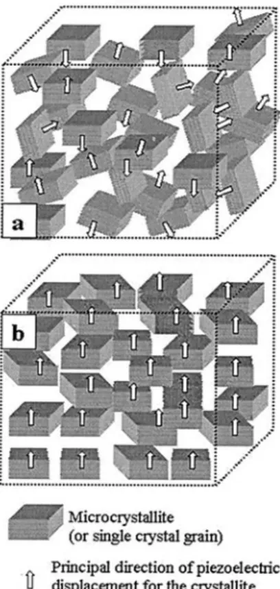
piezoelectric tensor and the direction of the applied electric field is required. Figure 1 shows a sche-matic representation of the piezoelectric effect for different microcrystallite organizations. The crys-tallites of Fig. 1共a兲 are randomly oriented. No over-all piezoelectric effect can be expected even if each crystallite shows piezoelectricity. In contrast, all the crystallites of Fig. 1共b兲 have the same orientation in the vertical direction, although in the horizontal plane crystallites do not present a preferred orienta-tion. In this case, if the vertical direction fits the piezoelectric tensor d and the applied electric field direction, one can expect the same piezoelectric dis-placement as for a single-crystal growth. For a par-tially organized growth, the expected piezoelectric effect is, of course, in between and depends on the ratio of well-oriented grains to all grains.3
2. Choice of Dielectric Material
Dielectric bulky materials with a piezoelectric effect higher than 100 pm兾V and that are absorption free in the optical telecommunications domain include Ba-TiO3 and Ta2O5. One major drawback of the first one is that it exhibits a considerable electro-optic effect共1640 pm兾V兲4, therefore it is strongly
polariza-tion dependent. In contrast, Ta2O5 is an excellent
candidate if one refers to optical properties: large
transparency domain, low scattering, and high me-chanical and chemical resistance,5,6at least for
amor-phous layers widely used for thin-film applications. The most stable form of crystallized Ta2O5 below 1360 °C7belongs to the orthorhombic class, and
val-ues of the piezoelectric tensor elements vary from zero to 200 pm兾V for d33where a displacement along
the third axis is expected when an electric field is applied parallel to this axis.
As mentioned above, the expected piezoelectric ef-fect for crystallized Ta2O5thin films depends on
mi-crocrystallite orientations and is, of course, lower than bulky values. Note that we chose to use amor-phous substrates共fused silica兲 and that we do not use the substrate crystalline lattice replication to help a single crystalline growth as occurs in epitaxy. This choice is justified because, as mentioned previously, our final goal is to deposit active layers within an optical thin-film stack, and we must not control the growth with the substrate. The underlying layer will be either amorphous or crystalline with a non-controlled orientation. Parameters able to influence the degree of organization of grains are therefore only thin-film deposition parameters共deposition rate, ox-ygen flow, substrate temperature, and annealing temperature兲.
3. Ta2O5Thin-Film Deposition
The deposition process used is electron-beam deposi-tion or convendeposi-tional reactive evaporadeposi-tion,8 with a
deposition temperature variable from ambient tem-perature to as high as 650 °C. We use a Balzers BAK-600 evaporation chamber to deposit Ta2O5 single layers on fused-silica substrates. Other processes suitable for piezoelectric layer deposition include pulsed laser deposition9,10or radio-frequency
sputter-ing.7,11 The deposition rate is controlled by a
quartz-crystal measurement unit, and the optical thickness of the reference substrate is controlled by an optical monitoring system at a wavelength of 600 nm 共see Fig. 2兲.
Both substrates are heated on the front sides with halogen lamps. On the rear side, one substrate is heated at high temperature with a resistive substrate heater. Affordable temperatures range from ambi-ent to as high as 950 °C, and a closed-loop regulation controls the resistive heater’s temperature via a K-type thermocouple. Calibration measurements have been performed to monitor the temperature on the deposition side of the substrate. The maximum reachable temperature is approximately 650 °C on the front side of a 2-mm-thick fused-silica substrate. Oxygen partial pressure in the chamber is also con-trolled. Material used for the evaporating process is Merck tantalum pentoxide tablets. Key parameters for optical and piezoelectric properties that we can act on are the deposition rate, O2flow, and substrate temperature. For all layers described in this paper, O2partial pressure is approximately 2⫻ 10⫺4mbar, which ensures a good stoichiometry and then good optical properties.
Fig. 1. 共a兲 Schematic drawing of a randomly oriented crystallite structure and共b兲 an organized structure with a preferred orienta-tion in the vertical direcorienta-tion If the piezoelectric tensor matches the vertical axis and the electric field direction, a piezoelectric dis-placement equivalent to the single-crystal structure disdis-placement can occur in the vertical direction.
4. Temperature Effect on Ta2O5Optical Properties
In accordance with the model of Movchan and Dem-chishin,12 the microstructure of the film layer
de-pends on the substrate temperature T during the deposition process and Tm, the melting point of
tan-talum pentoxide 共Tm ⫽ 1880 °C兲. The higher the substrate temperature is, the more energy adatoms have and the more mobility they have to re-arrange themselves in a stable crystalline form. We study here the influence of the film structure on the optical refractive index and scattering losses.
We consider three Ta2O5samples coated on fused silica, which are all t⫽ 375 nm thick. The first one 共S1兲 is coated at a 300 °C substrate temperature. The second one共S2兲 is coated at a 470 °C substrate temperature in the evaporation chamber, thanks to the resistive substrate heater. After characteriza-tions, this sample is annealed at 650 °C for 4 h共S3兲. At a deposition temperature of 300 °C, the film is totally amorphous. S2 is partially crystallized, and S3’s crystallinity is improved by the annealing pro-cess. From reflectance and transmittance measure-ments, we deduce the refractive index N as a function of wavelength.13 In the visible range, the imaginary
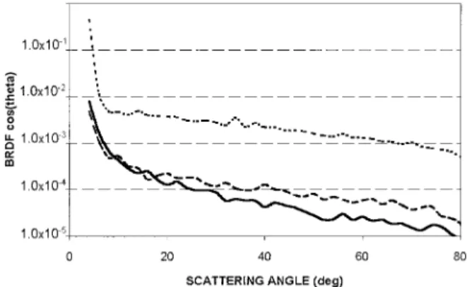
part of the refractive index is lower than 10⫺4. On Fig. 3 we have plotted deduced refractive indices N as a function of wavelength for S1, S2, and S3 in the 0.4 – 0.9m range. The major effect of an increasing temperature is the raising of the refractive index of the layers from N⫽ 2.06 to N ⫽ 2.24 at ⫽ 0.6 m. We deduce from light-scattering measurements that optical losses of S2 and S3 are essentially due to the light scattered by crystallites. The size of the grains, which will be discussed in Section 5, influ-ences this amount of scattered light. Scattering properties are investigated at normal incidence at a wavelength of 633 nm from 4° to 80° with an exper-imental setup described in Ref. 14. Results are plotted on Fig. 4. The general level of scattering increases with temperature, as the crystallization of
Ta2O5is improved. If we take the scattering level of
S1 as a reference, the average level of S2’s; scattered light is double, and the level of S3’s scattered light is approximately 50 times higher. Roughness at the two interfaces 共air–Ta2O5兲 and 共Ta2O5–substrate兲
and also the compactness of the film are probably the parameters influencing the amount of scattered light. Further research needs to be done to clarify the re-lation between film microstructure and light scatter-ing. Finally, these losses should be decreased with more compact layers. A more energetic deposition process such as ion assistance could be a solution, provided that the microstructure remains compatible with a piezoelectric effect.
5. Nonoptical Characterizations and the Expected Piezoelectric Effect
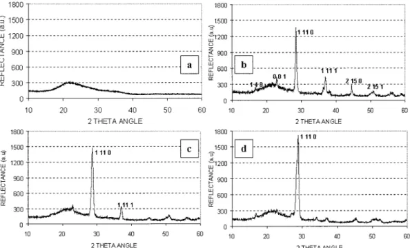
Nonoptical characterizations able to predict the pi-ezoelectric displacement of the film include x-ray dif-fraction 共XRD兲 diagrams and scanning electron microscopy 共SEM兲 images. XRD analysis is per-formed on a Philip’s X’Pert diffractometer. The ini-tial information given is the crystal structure of the Ta2O5particles used in the crucible for evaporation.
The Merck tantalum pentoxide tablets, whose mea-sured XRD spectrum is given on Fig. 5, are identified as belonging to the orthorhombic class.15 The lattice
Fig. 2. Evaporation chamber that uses the electron-beam depo-sition process. An optical monitoring and a quartz crystal mea-surement is performed on the reference substrate. The temperature of the heated substrate can reach 950 °C on the rear side.
Fig. 3. Calculated real parts of the refractive indices N for S1, S2, and S3 as a function of the wavelength.
Fig. 4. Bidirectional reflectance distribution function共BRDF兲 as a function of the measurement angle. Samples are illuminated under normal incidence.
parameters are a⫽ 0.6198 nm, b ⫽ 4.029 nm, c ⫽ 0.3888 nm, and␣ ⫽  ⫽ ␥ ⫽ 90°.
XRD and SEM analyses provide complementary information about the degree of crystallinity, the av-erage size of crystallites, and the overall texture of the film. We show results of a set of four samples of Ta2O5 thin films coated on fused-silica substrates.
The mechanical thickness of all samples is approxi-mately 375 nm. The substrate temperature during the deposition process was different for each sample. Sample S4共reference sample兲, coated at a 300 °C substrate temperature, is revealed to be totally amor-phous. No diffraction peak is visible on the XRD spectrum. 关Fig. 6共a兲兴. The shape of the spectrum is characteristic of the substrate atoms’ disposition 共here fused silica兲.
Sample S5 is a Ta2O5thin film coated on a 470 °C
heated substrate. Its XRD spectrum关Fig. 6共b兲兴 ex-hibits several diffraction peaks at particular angles,
defined by Ta2O5 crystal parameters. An
orthor-hombic crystal system is also identified. All peaks have different intensities, but no peak is really prom-inent. This indicates that the coating is polycrystal-line with a random grain orientation.
The temperature of the substrate for sample S6 is approximately 620 °C during the deposition process. In this case, increasing the adatoms’ energy permits them to re-arrange themselves in a more stable form, which improves crystallinity. We can see on the XRD spectrum of Fig. 6共c兲 that the intensity of the peak located at 2 ⫽ 28.6° has become much more important than the others. This means that the pro-portion of 共1 11 0兲 planes parallel to the substrate surface is higher than others, and therefore the layer exhibits a textured crystallized structure. We might be able to measure a small piezoelectric displacement for this sample, but it would be many times below the displacement of the same bulky layer.
The best-crystallized layer we deposited on a fused-silica substrate 共S7兲 has been obtained for a high substrate temperature around 650 °C and for a slow deposition rate of approximately 0.1 nm兾s. We can see on Fig. 6共d兲 that only one diffraction peak 共2 ⫽ 28.6°兲 is visible. This is characteristic of a well-textured film structure with a general orientation in the 共1 11 0兲 plane parallel to the substrate surface. S7 should present a noticeable piezoelectric effect.
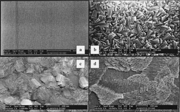
In addition to performing XRD analysis, we show SEM images of samples S4, S5, S6, and S7 achieved with an Oxford Instruments high-resolution scan-ning electron microscope on Fig. 7.
The SEM images give information about the film structure in agreement with the conclusion stated above. S4 is totally amorphous, crystallites of S5
Fig. 5. X-ray diffraction spectra of Ta2O5powder. Theta is the
angle between the incident light and the sample. 2theta is the angle between the incident light and the reflected beam in the inci-dent plane. The theoretical diffraction efficiency is also shown.
are randomly oriented, and S6 and especially S7 have a general orientation. We can also measure the mean grain size. For crystallized layers, the aver-age form of crystallites, measured on sample S6, is a parallelepipedal 100 nm long, 50 nm in width, and 10 nm in height. Unfortunately, pollution from the heater on the rear sides of the substrates did not permit us to perform optical characterizations on samples S5 to S7.
6. Interferometric Measurement of Piezoelectric Displacement
Among the different means available to measure pi-ezoelectric coefficients or pipi-ezoelectric displacements under an applied electric field, we can find interfero-metric measurement setups that give results as ac-curate as 0.1 pm.16 –18 At this time, we note that we
expect dimension changes for our thin films of ap-proximately 1 pm. We have chosen to implement a fiber interferometer that, as we will discuss in the following, is easy to use in terms of precise adjust-ments.
The setup we use is the extrinsic Fabry–Perot in-terferometer, previously reported in other papers.17,19
The general overview, of the instrument can be seen on Fig. 8. It is basically composed of a Y-monomode fiber coupler that performs the interferometer func-tion. The incoming light wave emitted by a tunable laser is coupled into the entrance fiber. At the end of the exit fiber共right side of the schematic兲, part of the light 共approximately 4%兲 is reflected backward be-cause of the refractive-index difference between the fiber core and the air; this wave is taken as the ref-erence wave. The other part of the light is coupled
out of the fiber, and the unique mode that was prop-agating through the fiber diverges. When a surface is facing the fiber exit, the diverging wave is reflected on this surface. Then a small part 共defined by a coefficient兲 of this coupled-out wave can be again coupled into the same exit fiber共measurement wave兲. If the optical path difference between what we called the reference wave and the measurement wave is below the laser coherence length, and because we use a monomode fiber, those two waves can interfere in-side the fiber. We use the last port of the coupler component, where 50% of the interfering light is transmitted, to detect the interference pattern.
As in any interferometer, the output intensity is
Fig. 7. Scanning electron microscopy of samples: 共a兲 S4, 共b兲 S5, 共c兲 S6, and 共d兲 S7.
Fig. 8. Extrinsic Fabry–Perot interferometer experimental setup. The photoreceptor measures the interference fringes between the sample and the glass–air interface of the fiber.
the square modulus of the sum of the two waves’ complex amplitudes. It can be expressed in Eq.共2兲 as
I⫽ I0关1 ⫹ m cos共兲兴, (2)
where m is the visibility of the interference pattern and is the phase difference between the waves given by
⫽ 4z兾. (3) We focus on the fact that depends both on the wavelength and on the distance z between the out-put of the fiber and the sample surface. Without giving further details, we note that m can be calcu-lated as a function of . As can be seen on Fig. 9, intensity on the photoreceptor changes when the dis-tance between the fiber output and the sample varies 共thick solid curve兲. Let us suppose that we apply an oscillating electric field E共oscillating at pulsation 兲 to our piezoelectric sample characterized by its piezo-electric coefficient d. This field involves an oscillat-ing displacement whose amplitude is given by⌬z⫽
d共E兲. Thus we measure the intensity variations ⌬I
with a lock-in amplifier at pulsation. We can cal-culate⌬Iby differentiating Eq.共2兲. This leads to
⌬I⫽ ⫺ I0m sin共兲
4
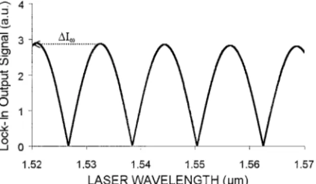
⌬z. (4) The visibility of piezoelectric-induced intensity vari-ations on the photoreceptor is affected by sin共兲. We use the wavelength tunability of our laser to set sin共兲 ⫽ 1 共peak values on Fig. 10兲. Thus, if we measure first the value of interferometric visibility
m, we can deduce⌬z.
We have performed calibration measurement on a piezoelectric lead zirconate titanate ceramics trans-ducer and measured displacements as small as a few tenths of a picometer. Below this limit, the signal is overwhelmed by noise. This noise originates both from the intensity noise of the laser and from the mechanical vibrations.
To characterize the samples described in Section 5, we deposited an electrode metallic coating on the top of each Ta2O5layer. The rear face of the substrate is
laid down onto a metallic plate, and then a high
volt-age共400 V兲 is applied between the two electrodes at frequency f0⫽ 兾2 ⫽ 105Hz. Given the thickness
of the substrate共2 mm兲, the electric field applied on the sample is 2 kV兾cm, much less than the break-down electric field. The voltage between the two sides of the Ta2O5layer共375-nm thickness兲 is 75 mV, and we measured a displacement of 1 pm for S7. The measurement curve 共having the same form as the simulated curve given on Fig. 10, which is a proof for the interferometric origin of the signal兲 after pro-cessing for conversion into displacement units is shown on Fig. 11. This value corresponds to a vari-ation of thickness approximately 13 pm兾V for a sand-wiched layer between two electrodes, much less than the possible 200 pm兾V for a single-crystalline Ta2O5
structure. The validity of the procedure is proven by repetition of the same protocol for S4 共amorphous layer兲, in which no f0 frequency displacement is de-tected共see Fig. 11兲.
7. Conclusion
Changing the coating deposition parameters and es-pecially heating the substrate temperature to as high as 650 °C during deposition enables us to obtain crys-tallized layers. We showed that Ta2O5 thin films
coated on an amorphous substrate heated above
Fig. 9. Theoretical intensity detected by a photoreceptor as a function of the distance z between the fiber exit and the sample
surface. Fig. 10. Principle of the measurement of a small f0displacement
from the intensity detected for two working points.
Fig. 11. Interferometric intensity measured as a function of the incident wavelength, the distance between the fiber and the sam-ple being constant共black curve兲. Under a 400-V voltage at f0⫽
105 Hz, we show the f
0-filtered signal for sample 7共dark gray
620 °C can present a preferred orientation compati-ble with a piezoelectric displacement on the growth axis. The greatest thickness variation we measured is approximately 13 pm兾V.
The study of optical properties for high-temperature coated or annealed Ta2O5 layers dem-onstrates not only a high refractive index 共approximately N ⫽ 2.25 at a wavelength of 600 nm兲 but also an increase in scattered light. These scat-tered losses depend on the size of the crystallites. Smaller grains or more compact layers with an as-sisted deposition process should improve the optical quality of layers. By optimizing deposition parame-ters, we should increase the piezoelectric effect of the layers and decrease the scattered light. The inser-tion of such layers into Fabry–Perot cavities with transparent conductive electrodes could be a way to tune the transmitted wavelengths for telecommuni-cation applitelecommuni-cations.1
We thank Carole Deumie for scattering measure-ments and for useful discussions.
This research is supported by Highwave Optical Technologies Marseille, Z.I. St Mitre, avenue de la Roche Fourcade, 13400 Aubagne, France, and by Le Conseil Re´gional Provence-Alpes-Coˆte-d’ Azur. References
1. M. Lequime, R. Parmentier, F. Lemarchand, and C. Amra, “Toward tunable thin-film filters for WDM applications,” Appl. Opt. 41, xxxx–xxxx共2002兲
2. W. P. Mason, Piezoelectric Crystals and Their Application to
Ultrasonics, 6th ed.共Van Nostrand, Princeton, N. J. 1964兲, pp.
40 – 46.
3. J. G. E. Gardeniers, Z. M. Rittersma, and G. J. Burger, “Pref-ered orientation and piezoelectricity in sputt“Pref-ered ZnO films,” J. Appl. Phys. 83, 7844 –7854共1998兲.
4. A. Yariv and P. Yeh, Optical Waves in Crystals共Wiley, New York, 1984兲, p. 233.
5. C. Chaneliere, J. L. Autran, R. A. B. Devine, and B. Balland, “Tantalum pentoxide thin films for advanced dielectric appli-cations,” Mater. Sci. Eng. 22, 269 –322共1998兲.
6. D. R. Lide, Handbook of Chemistry and Physics, 76th ed.共CRC Press, Boca Raton, Fla.,共1995兲.
7. B. R. Jooste and H. J. Viljoen, “A study of piezoelectric orthor-hombic Ta2O5,” J. Mater. Res. 13, 475– 482共1998兲.
8. H. K. Pulker and K. H. Guenther, “Reactive physical vapor deposition processes,” in Thin Films for Optical Systems, F. R. Flory, ed.共Marcel Dekker, New York, 1995兲, pp. 91–115. 9. S. Boughaba, G. I. Sproule, J. P. McCaffrey, M. Islam, and
M. J. Graham, “Synthesis of tantalum pentoxide films by pulsed laser deposition: material characterization and scale-up,” Thin Solid Films 358, 104 –113共2000兲.
10. J. Y. Zhang, Q. Fang, and I. W. Boyd, “Growth of tantalum pentoxide film by pulsed laser deposition,” Appl. Surf. Sci.
138 –139, 320 –324共1999兲.
11. T. Dimitrova, K. Arshak, and K. Atanassova, “Crystallization effects in oxygen annealed Ta2O5 thin films on Si,” Thin Solid Films 381, 31–38共2001兲.
12. B. A. Movchan and A. V. Demchishin, “Investigations of the structure and properties of thick Ni, Ti, W, Al2O3 and ZrO2 vacuum condensates,” Fiz. Met. Metalloved. 28, 653– 660 共1969兲.
13. J. P. Borgogno, B. Lazarides, and P. Roche, “An improved method for the determination of the extinction coefficient of thin film materials,” Thin Solid Films 102, 209 –220共1983兲. 14. C. Deumie, R. Richier, P. Dumas, and C. Amra, “Multiscale
roughness in optical multilayers: atomic force microscopy and light scattering,” Appl. Opt. 35, 5583–5594共1996兲. 15. International Centre for Diffraction Data, “Joint Committee
on Powder Diffraction Standards共JCPDS兲 Card No. 25-0922” 共ICDD, Newton Square, Pa. 共1996兲.
16. L. Burianova´, M. Sule, and M. Prokopova´, “Determination of the piezoelectric coefficients dijof PZT ceramics and
compos-ites by laser interferometry,” J. Eur. Ceram. Soc. 21, 1397– 1390共2001兲.
17. M. Schmidt, B. Werther, N. Fuerstenau, M. Mathias, and T. Melz, “Fiber-optic extrinsic Fabry–Perot interferometer strain sensor with ⬍50 pm displacement resolution using three-wavelength digital phase demodulation,” Opt. Express 8, 475– 480共2001兲.
18. N. Felix, D. Certon, F. Patat, and M. Lethiecq, “Piezoelectric materials, ultrasound transducers and arrays characterization by laser interferometry,” e-Journal Non-Destr. Test. Ultrason-ics 5共2000兲, www.ndt.net兾article兾v05n09兾felix兾felix.htm. 19. M. Lequime and J. J. Guerin, “Large OPD extrinsic Fabry–
Perot interferometers using thermally expanded core fiber,” in
European Workshop on Optical Fibre Sensors, B. Culshaw and