RESEARCH OUTPUTS / RÉSULTATS DE RECHERCHE
Author(s) - Auteur(s) :
Publication date - Date de publication :
Permanent link - Permalien :
Rights / License - Licence de droit d’auteur :
Bibliothèque Universitaire Moretus Plantin
Institutional Repository - Research Portal
Dépôt Institutionnel - Portail de la Recherche
researchportal.unamur.be
University of Namur
Glass and silicon probes
Castiaux, A.; Danzebrink, H. U.; Bouju, X.
Published in:Journal of Applied Physics DOI:
10.1063/1.368095 Publication date: 1998
Document Version
Publisher's PDF, also known as Version of record Link to publication
Citation for pulished version (HARVARD):
Castiaux, A, Danzebrink, HU & Bouju, X 1998, 'Glass and silicon probes: A comparative theoretical study for near-field optical microscopy', Journal of Applied Physics, vol. 84, no. 1, pp. 52-57.
https://doi.org/10.1063/1.368095
General rights
Copyright and moral rights for the publications made accessible in the public portal are retained by the authors and/or other copyright owners and it is a condition of accessing publications that users recognise and abide by the legal requirements associated with these rights. • Users may download and print one copy of any publication from the public portal for the purpose of private study or research. • You may not further distribute the material or use it for any profit-making activity or commercial gain
• You may freely distribute the URL identifying the publication in the public portal ?
Take down policy
If you believe that this document breaches copyright please contact us providing details, and we will remove access to the work immediately and investigate your claim.
Glass and silicon probes: A comparative theoretical study
for near-field optical microscopy
A. Castiaux,a)
Laboratoire de Physique du Solide, Fac. Univ. Notre-Dame de la Paix, 61, Rue de Bruxelles, B-5000 Namur, Belgium
H. U. Danzebrink
Physikalisch-Technische Bundesanstalt, Bundesallee 100, D-38116 Braunschweig, Germany
X. Bouju
Laboratoire de Physique Mole´culaire, U.M.R. C.N.R.S. 6624, Universite´ de Franche-Comte´, F-25030 Besanc¸on Cedex, France
~Received 12 December 1997; accepted for publication 26 March 1998!
Glass fibers, chemically etched at their extremities and covered with a thin metal coating, are often present in near-field optical microscopy. Such elongated systems can be used to either probe the evanescent components of the electromagnetic field at the surface of a sample, or locally couple this sample with optical evanescent waves. In this article, we analyze theoretically an alternative tip design made with a silicon core. This kind of probe could be very useful when infrared properties of a surface are to be investigated. The advantages of using such a material for near-field optical detection will be stressed and compared with the performances of a bulk glass fiber. © 1998
American Institute of Physics. @S0021-8979~98!02513-4#
I. INTRODUCTION
A significant part of the improvements realized for ten years in near-field optical instrumentation is due to the con-stant evolution of the design of probes used to detect near-field features at the surface of a sample. This element — key piece of all near-field instrumentation — establishes the bond between the experimentalist and the near-field optical phenomena to be observed. From the hole inside a metal screen1to the silicon nitride tetragonal tip2or the tetrahedral coated tip,3a lot of geometries and compositions were inves-tigated in order to build the best probe and to increase the resolution factor. This factor lies on a compromise between two crucial requirements, i.e., the detected intensity and the light confinement resulting from the tip-sample coupling. On one hand, one has to be able to measure weak field intensi-ties, on the other hand, this detection must be as localized as possible. Most of near-field microscopes are now equipped with glass fibers that were elongated and etched at their ex-tremity to obtain a very small scattering center at the apex. For a still better localization of the interaction zone, these glass fibers are often covered with a metallic coating, except a hole at the extremity.
The fabrication process of tips can lead to various shapes, more or less reproducible. Roughly, the extremity of the probe has a conical shape with a paraboloid apex. Al-ways for a confinement concern, very acute conical angles were investigated. However, such ‘‘pin’’ tips present an in-convenience. In emission as well as in detection, the light wave traveling inside the tip is early faced with the wave-guide cut-off frequency of the fiber, since its section is rap-idly decreasing. This problem is even more important when
the fiber is coated with metal because the boundary condi-tions are more drastic: the field has to fall to zero on the surface limiting the tip. For visible wavelength, it is possible to tackle the problem by using probes with a larger opening angle. Since the effective wavelength inside the probe is not large, the propagation inside the very tip is possible. How-ever, when higher wavelengths in the infrared spectrum are considered, usual tips cannot support electromagnetic modes far enough inside the tip, so that they are unusable in emis-sion as well as in detection. It is of prime importance to solve this problem and to find probe configurations that furnish a high resolution also in the infrared range,4because near-field infrared features meet more and more interest among the experimentalists.5,6 The developments of near-field spec-troscopy7–9 promise to obtain a better insight in infrared properties of high importance, especially in the studies of vibrational surface properties, or, more widely, of biological or medical applications.
Our purpose here is to highlight that a silicon tip pre-sents favorable properties to probe near-field phenomena in the infrared range. By comparing the illumination and col-lection efficiencies of glass and silicon probes in the near-infrared range, we will show the advantages of these new silicon probes.
II. NUMERICAL METHOD AND MODEL
We are faced with a macroscopic light-matter coupling problem where matter is defined by nontrivial boundaries and various dielectric constants. Different methods were al-ready implemented to solve Maxwell’s equations as pre-cisely as possible in such complicated geometries.10–13One of them, based on Green’s propagators, is particularly suited a!Electronic mail: [email protected]
52
to the study of near-field optics problems, where the interac-tions are localized in a given spatial region.14
A. Using Green dyadics to propagate the field
The first stage of this method is a discretization proce-dure of the material domains P involved in the interaction. Once this is done, the electromagnetic field is calculated at each discretization cell by solving the following self-consistent Lippmann–Schwinger equation thanks to an origi-nal algorithm15,16:
E~r,v!5E0~r,v!1
E
Pdr
8
G0~r,r8
,v!V~r8
,v!E~r8
,v!.~1! Here, E0(r,v) is the unperturbed electric field due to the
incident electromagnetic wave and E(r,v) is the total elec-tric field resulting from the light-matter interaction. The field at each perturbation cell is balanced by a potential V(r,v) that depends on the dielectric function at the considered cell. The same kind of equation can also be obtained for the mag-netic field H(r,v). Once we know the field in each discreti-zation cell, we can propagate it to any point r
8
of the refer-ence medium — the medium embedding the discretized regions — by considering each cell as a pointlike dipole. A Lippmann–Schwinger equation is once more requested to realize this propagation stage, this time without any problem of self-consistency. It is possible to know the electromag-netic field everywhere in the space, without any approxima-tion excepting the acuteness of the discretizaapproxima-tion procedure.B. Our model
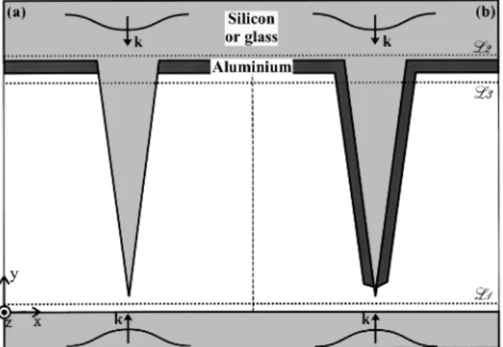
To compare the efficiency of glass and silicon tips in the near-infrared range, for an incident wavelength l05 1.3mm, we choose a two-dimensional model as the one
presented on Fig. 1. Inside the air junction between two semi-infinite dielectric media, we put a very sharp dielectric excrescence on one of the semi-infinite space and facing the
other one, to mimic a tip facing a sample. This excrescence is triangular, with an apex angle of 15° and a length of about 2 mm.
The dielectric media are glass (e5 2.25) or undoped silicon (e5 12.25), following the case that we want to in-vestigate. Another parameter is also taken into account: the presence or the absence of a metallic coating along the lateral borders of the tip. This coating is made of aluminum (e 52172.73 1i 32.47). The ~a! and ~b! parts of Fig. 1 re-spectively present the uncoated and coated models. Let us note that small metal screens are also included in the un-coated model. These screens surround the base of the dielec-tric excrescence in order to enhance the guiding process from or to this tip.
The incident light is simulated by a Gaussian wave ~FWHM5 4mm!. If we want to consider a collecting tip, this wave is incident from the lower semi-infinite medium. On the contrary, for an emitting tip, it comes from the upper semi-infinite medium.
A particularity of this computation is that the reference medium is not vacuum ~nor air!, but the dielectric material which the tip and both semi-infinite media are made of. This considerably reduces the importance of the discretized re-gion, that is, the air window and the metal screens. We can thus use a smaller discretization square mesh of 25 nm side. Moreover, since the tip support and the ‘‘sample’’ are semi-infinite, we avoid the reflections on the interfaces that usu-ally delimit the back of the tip or the sample. This makes the interpretation of the results easier.
The corrugated profile of the tip due to the discretization procedure could induce an artificial scattering. This can be avoided by considering that the square elements delimiting the probe are truncated by the line of the ideal profile and that the corresponding elements are weighted by the section of the partial area.17 Such an improvement could allow a better description of the electric field at the edges of the tip. In the present work, we focus on the behavior of the field in the neighborhood of the probe extremity and we choose to keep the profile as designed by the discretization.
III. RESULTS
Using the simulation method explained before, we ob-tain the distribution of the total electric field intensity uE(r,v)u2in the computation window described in Fig. 1, for a dielectric tip as well as for a metallized tip. Both emission and detection configurations are considered. Since we choose a two-dimensional model, we have to take into account the two fundamental polarizations, i.e., s-polarization, corre-sponding to an electric field along the translational invari-ance direction (z-axis!, and p-polarization, where the inci-dent electric field follows the x-axis~i.e., parallel to the plane of the image!. The propagation direction is along the y-axis. A.s-polarization
For this polarization, the light-matter problem can be resumed to a purely scalar calculation. As a matter of fact, the electric field E(r,v) keeps its polarization constant and is completely described by its modulus and phase.
FIG. 1. Model: a Gaussian wave is incident from the top~emitting tip! or the bottom~collecting tip! on a ~a! purely dielectric or ~b! metallized sharp tip.
53 J. Appl. Phys., Vol. 84, No. 1, 1 July 1998 Castiaux, Danzebrink, and Bouju
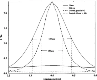
First, let us consider that the tip is used as an illumina-tion source. The incident wave comes from the upper semi-infinite dielectric medium on the tip apex. Since the effi-ciency of an emitting tip depends on the confinement and the intensity of the spot that it produces,18 we compute the in-tensity of the electric field on a line parallel to the x-axis and located just at the apex of the tip ~line L1 on Fig. 1!. The curves on Fig. 2 allow a comparison between the four con-sidered tips ~uncoated or coated glass or silicon tips!. With uncoated tips, the total electric field along lineL1 presents a maximum. This maximum is about 10 times larger for the silicon tip than for the glass one, due to the transparency of silicon at this infrared wavelength. The curves obtained with coated tips~dashed and long dashed curves, respectively, for glass and silicon cores! are amplified by a factor 66 in order to make the comparison easier. As a matter of fact, the met-allization makes the penetration of light inside the tip more difficult since the boundary conditions are more severe. The electric field must vanish at these limiting metallic surfaces and cannot extend outside, contrary to a purely dielectric tip. The spreading of light outside the dielectric tip depends on the constraint imposed on the incident wave by the narrow-ness of the tip. We can assimilate our tip to a succession of infinitesimal planar waveguides. To each of these local waveguides, i.e., to each y -coordinate of the tip, a cut-off wave number kcis associated, that becomes larger and larger as the tip narrows. When the wave vector modulus inside the guide is smaller than this kc, its component in the propaga-tion direcpropaga-tion y becomes imaginary and the propagapropaga-tion is no more allowed. This happens for a given yc level, under
which the waves inside the guide are evanescent. For a di-electric tip, light will still propagate by spreading outside the tip. However, when the tip is metallized, this spreading is not possible any more and only evanescent waves will remain in the lower part of the tip.
For the coated glass tip, this vanishing of propagating waves appears too far from the aperture, and no light is emit-ted by the tip, as it is shown by the dashed curve on Fig. 2.
On the contrary, the coated silicon tip allows a penetration of propagating waves almost down to the aperture, and the amount of emitted light is still significant. The principle is the same as the solid lens used in classical microscopy: by increasing the refraction index n of the medium, the resolu-tion is improved. Moreover, the coating concentrates the electric field below the tip apex, what is demonstrated by the diminution of the FWHM~180 and 100 nm for the uncoated and coated silicon tips, respectively!.
Let us consider now if the presence of an elongated tip has a positive effect on light confinement or if a simple hole in a metal screen — as the one we have at the base of the tip — would be so efficient. For this purpose, we present four more curves on Fig. 3 that will be compared with the previ-ous ones. These new curves describe the intensity of the electric field along line L3, once the wave begins its way inside the tip, i.e., the distribution of the field as if we had a hole in a metal screen. The first effect of the tip is a consid-erable intensity loss. This is particularly true for the coated glass probe ~dashed curves!: while the wave penetrating the tip presents a relatively high intensity, it is almost vanishing at the exit of the tip, for the reasons explained before. The tip acts also on the confinement of the incoming wave. For the dielectric probes~glass or silicon!, the exit field is less con-fined than the incoming one. The wave inclines to scatter outside the tip when it is submitted to a too high constraint by the boundaries of the tip. On the contrary, the confine-ment is improved through the metallized silicon tip. In this case, the tip canalizes the incoming wave, forcing it to stay on the inside and to acquire a better confinement. Finally, as already said, the coated glass tip has a dramatic effect, since the exit intensity is almost zero.
A last remark about the emission curves of Fig. 2 con-cerns the nonvanishing background intensity outside the tip-sample interaction zone. For dielectric tips, it is clearly due to the light spreading outside the tip, as we explained before. For coated tips, two phenomena can contribute to the illumi-nation of a larger surface portion. First, the metallization may be too thin and part of the incoming light could escape FIG. 2. Emission efficiency for glass and silicon tips, with and without an
aluminum coating. For the metallized tips, the emission curves are amplified by a factor 66.
FIG. 3. Penetration intensity for emitting glass and silicon tips, with and without an aluminum coating.
from the tip. However, this contribution must be very weak because aluminum has a low skin depth (d;50 nm for l 51.3mm!. We would rather indict a diffraction effect from the upper metal screens that do not extend beyond the com-putation window presented on Fig. 1. The incident wave skirts round the external limits of these screens, and adds its contribution to the illumination of the surface. This is a far-field effect.
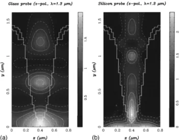
When the tip is used to detect near fields, the same con-ditions of confinement and intensity are requested for the tip-sample interaction. The computation of the fields in the near-field zone shows clearly that the confinement request is not fulfilled at all with an uncoated glass probe. On the other hand, a better confinement is obtained with an uncoated sili-con probe. This comparison is illustrated on the gray-scale maps given on Fig. 4. A Gaussian wave arriving from the sample on the glass probe interacts just a little with it, and continues its propagation up to the slit between the two small metal screens. When arriving on a silicon tip, the phenom-enon is stronger and the light is guided in the probe. How-ever, the interaction area is clearly around 250 to 300 nm. Even if it is well better than with the glass probe, we do not obtain near-field superresolution with our dielectric probe. Dielectric probes seem to need a priori high localization of the illumination zone to be effective. As it is mentioned be-fore, dielectric silicon tips are more interesting as illumina-tion sources.
An improvement of the confinement can be again ob-tained by coating the boundaries of the tip with metallic screens. An incident wave impinging this probe meets a small aperture and tries to penetrate inside the probe through it. Here the confinement is roughly limited by the size of the aperture and thus very good. The problem lies in the diffi-culty to detect sufficiently high intensities in the near-field zone. Since the effective wavelength of the incident wave is smaller in silicon than in glass, the penetration process is easier, and one can hope to detect a larger amount of light with a silicon tip than with a glass one. In order to put that in evidence, we compute the intensity of the electric field in the
detection zone, where the information is transmitted to the observer. The computation zone is drawn as line L2 on Fig. 1 and the intensity of the field along this line for both glass and silicon coated probes is plotted on Fig. 5. The continu-ous curve, corresponding to the glass probe, is vanishing in the center whereas a small intensity is present on the borders of the computation window. No light is coming from the tip itself, i.e., from the near-field interaction zone, while the in-cident wave skirts round the small screens to contribute to the lateral intensities. On the contrary, the dotted curve, due to the silicon probe, presents a small but appreciable central intensity, coming right from the near-field coupling zone by means of the probe. In the detection mode, a coated silicon probe should be more efficient in the infrared range. B. Extrapolation to three-dimensional interpretations
From the preceding study, we can infer some behaviors of the three-dimensional case, close to an experimental con-text. The two-dimensional computations show that the propagation of light inside the probe is submitted to cut-off conditions. Since the present probes can be considered as a succession of infinitesimal waveguides, the comparison be-tween the cut-off wave numbers kc of ideal metallized
waveguides~see Fig. 6! will help us to draw general conclu-sions from the two-dimensional study. The first column is FIG. 4. Distribution of the electric field intensity for dielectric detecting~a!
glass and~b! silicon probes.
FIG. 5. Detection efficiency inside a glass or a silicon probe coated with aluminum.
FIG. 6. Cut–off wave numbers for~a! a planar metallized waveguide, ~b! a square metallized waveguide, and~c! a cylindrical metallized waveguide.
55 J. Appl. Phys., Vol. 84, No. 1, 1 July 1998 Castiaux, Danzebrink, and Bouju
dedicated to a planar waveguide, the basis of our two-dimensional model. Its thickness is d and the borders are perfect metal plates. The second column concerns a square waveguide, of side d. The last column is for a cylindrical waveguide, which can be related to three-dimensional probes. Its diameter is d.jmn andjmn
8
are the nth zeros of,respectively, the cylindrical Bessel function Jm and its
de-rivative Jm
8
. All these cut-off wave numbers are easily found by using the boundary conditions.19 If we look at the small-est kcd value, associated with the first mode, we obtain kcd5p for modes TE1 and TM1 in the planar waveguide, as
well as for modes TE01 and TM01 in the square waveguide.
For the cylindrical geometry, the first mode is mode TE11,
for which kcd52j11
8
53.6. Thus the study of thetwo-dimensional geometry gives a rather optimistic point of view, since the cut-off conditions in three-dimensional guides are more severe. Propagation will even be forbidden with larger diameters tips and the decay of evanescent waves will be more fast. So we can extrapolate our conclusions to the three-dimensional case: for near-infrared wavelengths, a silicon probe will be highly more interesting than a glass probe, because the wave vector modulus k52pn/l0,
de-pending on the index n, is easily larger than kc.
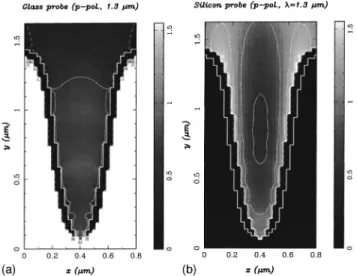
In order to be complete, we must note that the coatings are not made of perfect metals and are not perfectly flat. On one hand, real metals will lead to a skin effect: light will penetrate inside the metal layer on a small fraction of the wavelength and wall losses will occur, reducing the total intensity of the propagating beam. Since we use experimen-tal dielectric functions20to describe the metallic zones in our model, this effect is included in our preceding computations. On the other hand, surface roughnesses will act as scattering centers, producing local enhancements of field intensity. This happens only when there are field components normal to the surface. In a three-dimensional tip, this is always the case. Our preceding computations do not show such surface en-hancement, because the s-polarized field is always parallel to the dielectric-metal interfaces. The only way to take this ef-fect into account in our two-dimensional simulations is to consider a p-polarized incident wave. Two illustrations, pre-sented on Fig. 7, compare the detection process with coated probes that are respectively made of glass and silicon. Obvi-ously, a few light penetrates inside the glass probe, whereas the major part of the incident wave skirts round the tip. The intensity level around the tip is saturated to the maximal value that we imposed to align the scales of both computa-tions. On the contrary, the coupling with the silicon probe is efficient: most part of the incident light penetrates inside the tip. The local excitations on the metal boundaries are present in both illustrations. For the glass probe, the external surface shows enhancements of the field where the incident wave meets roughnesses. The same kind of excitations are present inside the silicon probe, since the incident wave penetrates it and is more intense on this inner interface. These illustra-tions indicate that silicon probes, once more, could be more efficient than glass probes in the detection process. Identical comparisons can be done in p-polarization for the emission case.
IV. CONCLUSIONS
Thanks to a two-dimensional model, we highlight the efficiency of silicon probes when they are used to study near-field features in the near-infrared range. A comparison with usual glass probes indicate clearly the advantages of silicon probes as an illumination as well as a detection tool. Espe-cially, aluminum coated silicon probes show a possible reso-lution around 100 nm, i.e., less thanl/13.
Since our model is two-dimensional, reservations must be made in respect of quantitative conclusions. However, in order to be able to generalize our qualitative analysis to a three-dimensional reality, we study both s- and
p-polarizations. The interest of silicon as probe material is
obvious in both cases. We also demonstrate that the use of silicon probes could even be more interesting when three-dimensional probes are involved, since the cut-off problem that makes glass probes unuseful in the infrared spectrum is more crucial when the wave must travel in such a three-dimensional probe.
We deliberately chose a very narrow, acute tip, in order to accentuate the cut-off effects. Near-infrared properties were already studied using tapered glass probes21,22and the obtained results were still interesting. However, the propaga-tion problems presented in this article can only be more im-portant when the wavelength increases. Alternative methods to probe the near-field must be elaborated to be able to face these problems. Our purpose here was essentially to propose such a solution, particularly suited for the extension of near-field optics to higher wavelengths: high refractive index probe materials.
ACKNOWLEDGMENTS
The authors want to warmly thank Dr. Ch. Girard ~Uni-versity of Toulouse, France!, for numerous fruitful discus-sions. One of the authors ~A.C.! is grateful to the Belgian National Foundation for Research ~F.N.R.S.! for financial FIG. 7. Distribution of the electric field intensity in the near–field zone, when a coated~a! glass or ~b! silicon probe is detecting a Gaussian incident wave.
support. This work was realized as part of the Human Capital and Mobility program of the European Community.
1U. Du¨rig, D. W. Pohl, and F. Rohner, J. Appl. Phys. 59, 3318~1986!. 2
N. F. Van Hulst, M. H. P. Moers, and B. Bo¨gler, J. Microsc. 171, 95
~1993!.
3J. Koglin, U. C. Fischer, and H. Fuchs, Phys. Rev. B 55, 7977~1997!. 4A. Lahrech, R. Bachelot, P. Gleizes, and A. Boccara, Opt. Lett. 21, 1315
~1996!.
5
H. U. Danzebrink, A. Castiaux, Ch. Girard, X. Bouju, and G. Wilkening, Ultramicroscopy 71, 373~1998!.
6A. Lahrech, R. Bachelot, P. Gleizes, and A. Boccara, Appl. Phys. Lett. 71,
575~1997!.
7
J. K. Trautman, J. J. Macklin, L. E. Brus, and E. Betzig, Nature~London!
369, 40~1994!.
8Y. Toda, M. Kourogi, and M. Ohtsu, Appl. Phys. Lett. 69, 827~1996!. 9A. Richter, G. Behme, M. Su¨ptitz, Ch. Lienau, and T. Elsaesser, Phys.
Rev. Lett. 79, 2145~1997!. 10
R. Carminati and J.-J. Greffet, Opt. Commun. 116, 316~1995!.
11D. Barchiesi and D. Van Labeke, Ultramicroscopy 57, 196~1995!. 12L. Novotny, D. W. Pohy, and B. Hecht, Opt. Lett. 20, 970~1995!. 13Ch. Girard and A. Dereux, Rep. Prog. Phys. 59, 657~1996!. 14
O. J. F. Martin, Ch. Girard, and A. Dereux, Phys. Rev. Lett. 74, 526
~1995!.
15O. J. F. Martin, A. Dereux, and Ch. Girard, J. Opt. Soc. Am. A 11, 1073
~1994!.
16A. Castiaux, Ch. Girard, A. Dereux O. J. F. Martin, and J.-P. Vigneron, Phys. Rev. E 54, 5752~1996!.
17
Ch. Girard and O. J. F. Martin~private communication!. 18
O. J. F. Martin and Ch. Girard, Appl. Phys. Lett. 70, 705~1997!. 19J. A. Kong, Theory of Electromagnetic Waves~Wiley, New York, 1975!. 20E. D. Palik, Handbook of Optical Constants of Solids ~Academic, San
Diego, 1991!.
21R. S. Decca, H. D. Drew, and K. L. Empson, Appl. Phys. Lett. 70, 1932
~1997!.
22
W. D. Herzog, M. S. U¨ nlu¨, B. B. Goldberg, G. H. Rhodes, and C. Harder, Appl. Phys. Lett. 70, 688~1997!.
57 J. Appl. Phys., Vol. 84, No. 1, 1 July 1998 Castiaux, Danzebrink, and Bouju