Ministry of Higher Education and Scientific Research
University of Batna 2 – Mostefa Ben Boulaïd
Faculty of Technology
Department of Electronics
Dissertation
Prepared within the Advanced Electronics Laboratory (LEA)
Presented in fulfillment of the requirement of the degree of:
Doctor of Science in Electronics
Option: Microelectronics
Entitled:Contribution to study and modeling of the nanoscale
multi-gate transistor using neural and evolutionary techniques
Presented by:
Elasaad CHEBAKI
Before the jury composed of:
M. Abdelhamid BENHAYA Prof. University of Batna 2 Chairman
M. Fayçal DJEFFAL Prof. University of Batna 2 Advisor
M. Ramdane MAHAMDI Prof. University of Batna 2 Examiner
M. Abdesselam HOCINI Prof. University of M'Sila Examiner
M. Djamel KHEDROUCHE Assoc. Prof. University of M'Sila Examiner M. Djamil RECHEM Assoc. Prof. University of Oum El Bouaghi Examiner
Université de Batna 2 – Mostefa Ben Boulaïd
Faculté de Technologie
Département d’Electronique
Thèse
Préparée au sein du Laboratoire d'Electronique Avancée (LEA)
Présentée pour l‟obtention du titre de:
Docteur en Sciences en Électronique
Option : Microélectronique
Sous le Thème:
Contribution à l’étude et la modélisation du transistor
nanométrique à multi-grille en utilisant les techniques
neuronales et évolutionnaires
Présentée par:
Elasaad CHEBAKI
Devant le jury composé de:
M. Abdelhamid BENHAYA Prof. Université de Batna 2 Président
M. Fayçal DJEFFAL Prof. Université de Batna 2 Rapporteur
M. Ramdane MAHAMDI Prof. Université de Batna 2 Examinateur M. Abdesselam HOCINI Prof. Université de M'Sila Examinateur
M. Djamel KHEDROUCHE MCA Université de M'Sila Examinateur
M. Djamil RECHEM MCA Université de Oum El Bouaghi Examinateur
In The Name Of Allah The Most
Beneficent The Most Merciful
Au Nom D'Allah Le Tout Miséricordieux Le
Très Miséricordieux
This dissertation is dedicated to my best friend, my most
loyal companion, my beautiful amazing life companion.
The one person who knew me, the one person who protected
me, the primary reason to any of my achievements, the one
person who I loved unconditionally. The true love of my
life- my mother-.
Acknowledgments
First of all, I am deeply grateful to The Almighty Allah (SWT), the Most High, the Most Compassionate, and the Most Merciful for all his giving and for the opportunity He gave me to study, to research and to write and finalizing this Ph.D. project. I Thank Allah, my utmost thanks, for providing me this opportunity and granting me the capability to proceed successfully.
I cannot express enough thanks to my supervisor Professor Fayçal DJEFFAL, who accepted me as his Ph.D. student at the Department of Electronics, supported my whole graduate life, suggested the topic and provided the platform to complete the project, helped in every step of the way, always believed in me and never hesitate to provide relentless support and motivation at all times throughout all these years. My completion of this work could not have been accomplished without his deepest expertise and the most shrewder insight. Many thanks for his permanent availability and responsiveness to my requests and for giving his time and effort without reservation. I would also like to express my appreciation for his guidance during my study. Without which this research would never have reached this point. And assisting me throughout my thesis-writing period; providing encouragement, good company, and lots of good ideas I‟m grateful for all scientific discussion we had and for giving me his inestimable advice and valuable guidance during different cycles of my studies M.Sc and Dr.Sc. I have really learned a lot from his comments and suggestions.
I would like to thank Professor Abdelhamid BENHAYA from the University of Batna-2- for being president of the examination committee. I thank my oral thesis committee members, Professor Ramdane MAHAMDI from University of Batna -2- , Professor
Abdesselam HOCINI and Dr. Djamel KHEDROUCHE from University of M'Sila, and Dr. Djamil RECHEM from University of Oum El Bouaghi, for accepting, taking time to
serve as committee members, to review my dissertation and give valuable comments.. I am really grateful to all my lab members and colleagues Dr. T. BENTRCIA, Mr. H. FERHATI and Mr. A. AOUF for their advice and their willingness to share their bright thoughts with me, for shaping up my research.
Finally, I would like to take this opportunity to thank all my friends and colleagues and the staff at the Department of Electronics, University of Batna -2- who have given their support and helped me in completing this work.
If I did not mention someone‟s name here, it does not mean that I do not acknowledge your support and help. Again, I would like to thank everyone who supported and helped me during my Ph.D. study.
Abstract
The downscaling of the transistor dimensions was the main and the most important factor leading to improvements in integrated-circuit performance and cost, which contributes to the rapid development of the semiconductor industry. In this dissertation, firstly we propose a new design of Double Gate Junctionless (DGJL) MOSFET based on both gate material engineering and highly doped of drain/source extensions. Analytical models associated to the drain current, analog and radio-frequency (RF) performance parameters are developed incorporating the impact of dual-material gate engineering and two highly doped extension regions on the analog/RF performance of DGJL MOSFET. The transistor performance figures-of-merit (FOM), governing the analog/RF behavior, is also analyzed. The study findings concerning the analog/RF performance are discussed and compared between the proposed design and a conventional DGJL MOSFET of similar dimensions, where the proposed device shows excellent ability in improving the analog/RF performance and provides higher drain current and improved figures-of-merit as compared to the conventional DGJL MOSFET. The obtained results are validated against the data obtained from TCAD software for a wide range of design parameters. Moreover, the developed analytical models are used as a mono-objective function to optimize the device analog/RF performance using Genetic Algorithms (GAs). In comparison with the reported numerical data for Inversion-Mode (IM) DG MOSFET, our optimized performance metrics for JL device exhibits enhancement over the reported data for IM device at the same channel length. This dissertation also focuses on the immunity behavior of the junctionless DG MOSFET device against the hot carrier degradation effect. As a result, we demonstrate that the junctionless DG MOSFET can be a viable option to enhance the immunity performances of nanoscale CMOS-based devices technology for nanoelectronics digital applications.
Keywords: Modeling, Optimization, Multigate, Double Gate, Analog, Radio Frequency, Nanoscale, Dual Material Gate, Genetic algorithm.
Résumé
La miniaturisation des dimensions du transistor était le facteur principal et le plus important menant aux améliorations des performances et du coût du circuit intégré contribuant au développement rapide de l'industrie des semi-conducteurs. Dans cette thèse, nous proposons tout d'abord une nouvelle structure MOSFET à double grille sans jonction (DGJL) basée à la fois sur la grille double matériaux et les extensions fortement dopées liées aux drain et source. Des modèles analytiques associés au courant de drain, aux paramètres de performance analogique et radiofréquence (RF) sont développés en incorporant l'impact d'une grille à deux matériaux et deux régions d'extension fortement dopées sur les performances analogique/RF du MOSFET DGJL. Les facteurs de mérite (FOM) du transistor, qui régissent le comportement analogique/RF, sont également analysées. Les résultats de notre étude concernant les performances analogique/RF pour la structure proposée sont discutés et comparés avec ceux d‟un MOSFET DGJL conventionnel de dimensions similaires, où le dispositif proposé présente une excellente capacité à améliorer ces performances, et fournit un courant de drain plus élevé. Les résultats délivrés sont validés par rapport aux données obtenues à partir du logiciel TCAD pour une large gamme de paramètres de conception. De plus, les modèles analytiques développés ont été adoptés comme une fonction objectif pour optimiser les performances analogique/RF du dispositif en utilisant les Algorithmes Génétiques (AGs). En comparaison avec les données numériques rapportées pour la structure MOSFET en mode d‟Inversion (IM), nos paramètres de performance optimisés pour le dispositif JL présentent une amélioration en comparaison avec le dispositif en mode d'inversion. Cette thèse s‟occupe également de l'immunité du dispositif DG MOSFET sans jonctions envers l'effet de dégradation initié par les porteurs chauds. En conséquence, nous avons démontré que le DG MOSFET sans jonctions peut être un choix fiable pour améliorer les performances relatives aux transistors MOSFET à l'échelle nanométrique pour les applications numériques.
Mots clés : Modélisation, Optimisation, Grilles Multiples, Double Grille, Analogique, Radio Fréquence, Echelle nanométrique, Grille double matériaux, Algorithme génétique.
صخلم
تديذًنا شئأذنا ءادأ ًف ٍٍغحخنا ىنإ يدؤٌ يزنا ىْلأأ ظٍئشنا مياعنا ًْ سٕخعضَاشخنا داعبأ ىدح ضٍهقح تنٔاحي ٌإ ثلاطًٕنا ِابشأ تعاُظن عٌشغنا سٕطخنا ًف ىْاغٌ يزنا شيلأا ،آخفهكح ضٍفخح ٔ ( مقإُنا فاظَأ ) . ِزْ ًف ىًٍظح ذشخقَ لأأ ،تحٔشطلأا ا سٕخعضَاشخن اذٌذخ ٌٕكي ثلاطٔ ٌٔذب تبإبنا ًئاُث ٍي مك طاعأ ىهع تٍئاُث تبإب ٌداعًنا بظًنا ٔ عبًُنا يداذخيا ٍي مكن ًناع بٌٕشح ٔ . صاخ تٍهٍهحح جراًَ شٌٕطح ىح اًك ة ،سٕخعضَاشخنا عبُي ساٍخب ٍٍغحح ىح اضٌأ ٔ تٍكهعلانا ثاددشخنا ًنادي ٍي مك ًف سٕخعضَاشخنا ءادأ شٌٍاعي ٔ د عي تٌشظاُخنا ثاساشلإا شٍثأح حي لا ٍي مك ٌداعًنا تٍئاُث تبإب ًناعنا بٌٕشخنا ثار بظًنا ٔ عبًُنا يداذخيا ٔ . اشٍثأح شثكلأا ءادلأا شٌٍاعي مٍهحح ىح اًك تٍكهعلانا ثاددشخنا ٔ تٌشظاُخنا ثلااًعخعلاا ِادح ّكٕهع ضخٌ اًٍف سٕخعضَاشخهن . ًف آٍهع مظحخًنا حئاخُنا اضٌأ لذعًنا ٔ ذشخقًنا ىًٍظخنا ٍٍب آخَساقي ىحٔ جشقَٕ تٍكهعلانا ثاددشخنا ٔ تٌشظاُخنا ثلااًعخعلاا ضخٌ اي ًف اُخعاسد تهثاًخي داعبأب كنر ٔ ًكٍعلاكنا ىًٍظخنا ٍٍب ٔ ( ةاُقنا لٕط ظفَ ) ًف ةصاخًي ةسذق ذشخقًنا سٕخعضَاشخنا ىطعأ ثٍح ، تٍكهعلانا ثاددشخنا ٔ تٌشظاُخنا ثلااًعخعلاا لادي . كنر ٔ آٍهع لٕظحنا ىح ًخنا حئاخُنا تحط ٍي ققحخنا ىح حياَشب تطعإب آٍهع مظحخًنا حئاخُنا مباقي آخَساقًب فهٍعا تفهخخي ضئاظخب ٔ ىًٍظخهن تععأ تعًٕدًن ٕكا . لإابٔ تفاض تٍثاسٕنا ثاٍيصسإخنا ًف فذْ لأذك آٍهع مظحخًنا تٍهٍهحخنا جراًُنا واذخخعا ىح ،كنر ىنإ ( تٍٍُدنا ) ٔ تٍكهعلانا ثاددشخنا ًف بكشًنا ءادأ تٍهثيأ ٍٍغحخن كنر ٔ تٌشظاُخنا ثاساشلإا ىح ًخنا تًٍقشنا ثاَاٍبنا عي تَساقًناب ءادلأا شٌٍاعي ٌئف ،ًكٍعلاكنا سٕخعضَاشخنا مخأ ٍي اْشكر ( ةدٕدنا ) ٌٔذب ذشخقًنا سٕخعضَاشخناب تطاخنا تُغحًنا ثلاطٔ JL سٕخعضَاشخنا ٍي ٍٍعُٕنا ٍٍب تَساقًناب كنر ىح ٔ ٍغحأ حئاخَ ىطعأ ( ذشخقًنا ٔ ًكٍعلاكنا ) ظفَ ىهع ةاُقنا لٕط . تعاُي ىهع اضٌأ تحٔشطلأا ِزْ ًف ضكشَٔ سٕخعضَاشخنا ثلاطٔ ٌٔذب تبإبنا ًئاُث شٍثأح ذض فشعٌ اي تُخاغنا ثاُحشناب . سٕخعضَاشخنا ٌأ اٍُب ،كنزن تدٍخَٔ ذشخقًنا ثلاطٔ ٌٔذب تبإبنا ًئاُث لاباق اساٍخ ٌٕكٌ ٌأ ٍكًٌ ًف تًٍقشنا ثاقٍبطخنا ٔ كٍَٔشخكنإ َٕاُنا ًف تهًعخغًنا ٔ تًئاقنا ةضٓخلأا اٍخٕنُٕكح ٍي تعَاًًنا ءادأ ضٌضعخن قٍبطخهن يشخيَٕاُنا ىهغنا . حيتافملا تاملك : تٌشظاُخنا ثاساشلإا ،تبإبنا ًئاُث ،ثابإبنا دذعخي ،تٍهثيلأا ،تخزًُنا ( تٍهثاًخنا ) ىهع ،ًكهعلا ددشح ، تٍٍُدنا تٍيصسإخنا ،ٌداعًنا تٍئاُث تبإب ،يشخيَٕاَ .Contents Acknowledgments ... (i) Abstract ... (iii) Résumé ... (iv) ضخهي ... (v) Contents ... (vi) List of figures ... (x) List of tables ... (xv)
Related publications work ... (xvi)
Introduction ... 1
Layout of the Thesis ... 3
Chapter I: MOSFET Transistor: miniaturization limits and solutions ... 5
I.1 Introduction ... 6
I.2 Description of the MOS transistor ... 7
I.2.1 The MOS structure ... 7
I.2.2 Principles operating regimes ... 8
I.3 SOI technology ... 14
I.3.1 SOI technology with a single Gate ... 14
I.3.2 Multi-gate transistors ... 19
I.4 Double-Gate MOSFET architecture ... 22
I.5 Gate-All-Around MOSFET architecture ... 24
I.5.1 Different categories of GAA MOSFET technology ... 26
I.5.2 Electrical properties of GAA MOSFET ... 30
I.6 Conclusion ... 34
Chapter II: Soft Computing based methods ... 48
II.1.1 Soft Computing as the fusion of several preexisting techniques ... 36
II.1.2 Soft Computing as an antithesis of Hard Computing ... 39
II.1.3 Soft Computing as a tool for outfacing with imprecision and uncertainty ... 39
II.1.4 Soft Computing defined by essential characteristics ... 41
II.2 Introduction to Fuzzy logic ... 41
II.2.1 Basic concept ... 42
II.2.2 Fuzzy sets ... 42
II.2.3 Membership functions ... 44
II.2.4 Fuzzy set operations ... 49
II.2.5 Fuzzy logic rules ... 51
II.2.6 Fuzzy logic model ... 52
II.3 Artificial Neural Networks ... 56
II.3.1 Biological Neuron ... 56
II.3.2 Artificial Neuron (The Perceptron) ... 57
II.3.3 Transfer Functions ... 61
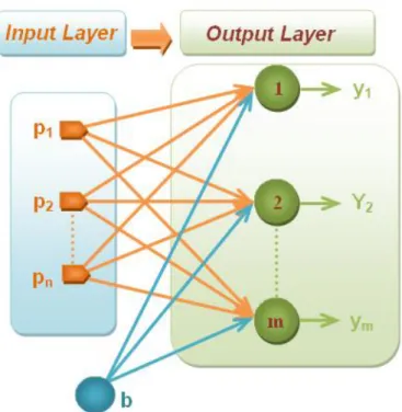
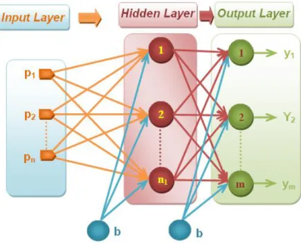
II.3.4 Network Architectures ... 62
II.3.5 Training Processes and Properties of Learning ... 68
II.3.5.1 Supervised Learning ... 69
II.3.5.2 Unsupervised Learning ... 69
II.3.5.3 Reinforcement Learning ... 70
II.4 Genetic algorithm (introduction) ... 70
II.4.1 Biological Background and notation ... 71
II.4.2 Basic concept ... 71
II.4.3 Encoding technique ... 74
II.4.4 Evaluating fitness ... 75
II.4.6 Crossover operators ... 77
II.4.7 Mutation operators ... 80
II.4.8 Replacement operators ... 81
II.4.9 Convergence criteria ... 81
II.5 Hybrid Soft Computing ... 82
II.5.1 Hybridization rules ... 82
II.5.2 Possibilities of integrating two techniques ... 83
II.5.3 Neuro-fuzzy systems ... 85
II.5.4 Adaptive Neuro-Fuzzy Inference Systems (ANFIS) ... 86
II.6 Conclusion ... 86
Chapter III: New DGJL MOSFET design to improve analog/RF performance ... 87
III.1 Introduction ... 88
III.2 Modeling methodology ... 90
III.2.1 Drain current model ... 90
III.2.2 Analog/RF parameter models ... 96
III.3 Results and discussions ... 97
III.3.1 Optimization of DGJL MOSFET performance ... 104
III.4 Conclusion ... 106
Chapter IV: Design of DGJL MOSFETs for nanoscale circuit applications ... 108
IV.1 Introduction ... 109
Part (1): Two-dimensional numerical analysis of nanoscale junctionless and conventional Double Gate MOSFETs including the effect of interfacial traps ... 110
IV.1.1 Introduction ... 110
IV.1.2 Numerical simulations ... 111
IV.1.3 Results and discussions ... 113
Part (2): Impact of gate material engineering and highly doped drain/source extensions in
DGJL MOSFET on nanoscale circuit performances ... 115
IV.2.1 Introduction ... 115
IV.2.2 Numerical simulations ... 116
IV.2.2.1 Device design ... 116
IV.2.2.2 Simulation models ... 118
IV.2.2.3 Inverter circuit design ... 119
IV.2.3 Results and discussion ... 119
IV.2.4 Conclusion ... 122
Chapter V: ANFIS-based Approach to Predict the Degradation-related Ageing of Junctionless GAA MOSFET ... 123
V.1 Introduction ... 124
V.2 Numerical simulations ... 125
V.3 ANFIS based approach ... 127
V.4 Results and discussion ... 129
V.5 Conclusion ... 137
VI Conclusions and future work ... 139
VI. 1 Contributions and conclusion ... 139
VI. 2 Suggestions for future work ... 141
List of figures
I.1: Illustration of the die map of: (a) 𝐼𝑛𝑡𝑒𝑙 4004 processor (b) 𝐼𝑛𝑡𝑒𝑙 𝐶𝑜𝑟𝑒 𝑖9 −
7980𝑋𝐸 processor ... 06
I.1. Die map of: (a) 𝐼𝑛𝑡𝑒𝑙 4004 processor (b) 𝐼𝑛𝑡𝑒𝑙 𝐶𝑜𝑟𝑒 𝑖9 − 7980𝑋𝐸 processor. ... 06
I.2. N-type MOS transistor: (a) perspective view, (b) cross-section. ... 07
I.3. Energy band diagrams of an n-type 𝑀𝑂𝑆 transistor. ... 09
I.4. Comparison between Modeling and Measurement of Linear Drain Current for a MOS Transistor with Ultra Thin Oxide Tox = 2.1nm (a) MOS with Long N- type channel (Weff/Leff = 10/10μm) and (b) MOS with short N- type channel (Weff/Leff = 10/0.13μm) . ... 13
I.5. Comparison between Modeling and Drain Current Measurement vs. Drain Voltage for Different Gate Voltage Values for a MOS Transistor with Ultra Thin Oxide Tox = 2.1nm (a)MOS with Long N- type channel (Weff/Leff = 10/10μm) and (b) MOS with short N- type channel (Weff/Leff = 10/0.13μm) ... 14
I.6: Cross-section Schematic view of MOS transistors (a) bulk and (b) SOI. ... 15
I.7. Schematic representation of a SOI transistor: (a) fully depleted and (b) partially depleted ... 15
I.8. Distribution of the depletion charge for bulk MOSFET and SOI. ... 17
I.9. Capacitive equivalent circuit (a) of a bulk MOSFET and (b) of a SOI ... 17
I.10. Comparison of the subthreshold slope of the MOS transistor in bulk and SOI technologies, for a constant geometry. ... 18
I.11. Electrostatic influence on SOI with a single gate. ... 19
I.12. Evolution of SOI technology over the years. ... 19
I.13: Single gate versus various multi-gate structures: (a) Single-Gate SOI, (b)Double-Gate SOI, (c) Tri-(b)Double-Gate SOI, (d) Π (b)Double-Gate, (e)Quadruple-(b)Double-Gate SOI, (f) Surrounding-(b)Double-Gate SOI. ... 20
I.14: Extension of the gates leading to the structures Π and Ω SOI MOSFETs ... 21
I.15: DG MOSFETs topologies: (a) Planar type; (b) Vertical type; (c) Fin FET ... 23
I.17. (a) top view of the layout of a GAA MOSFET. (b) Cross-section view with SEM of
triangular GAA MOSFET with dimensions (c) 3D diagram of GAA MOSFET. ... 26
I.18: FIB-SEM cross-section images of (a) triangular GAA MOSFET, and (b) pentagonal GAA MOSFET ... 27
I.19: Simplified steps of realization (cross-sections of the channel) of the triangular, pentagonal, and Ω-gate transistors [53] ... 27
I.20. (a) 3D schematic view of the GAA MOSFET transistor (b) sectional view of the DG MOSFET (c) 3D schematic view of the (SOI) FinFET transistor. ... 28
I.21. 3D and Cross-section view of the Square GAA MOSFET with 1-channel. ... 28
I.22. (a) 3D diagram of TSNWFET GAA transistor (b) TEM cross-section images of TSNWFET. ... 29
I.23. (a) TEM cross-section image of the n-MCFET transistor with 5 channels ... 29
I.24. SEM image of a vertical transistor with a thickness of ~ 20 nm and a height of 1μm. ... 30
I.25. Cylindrical GAA MOSFET (a) component structure in 3D (b) Cross-section. ... 30
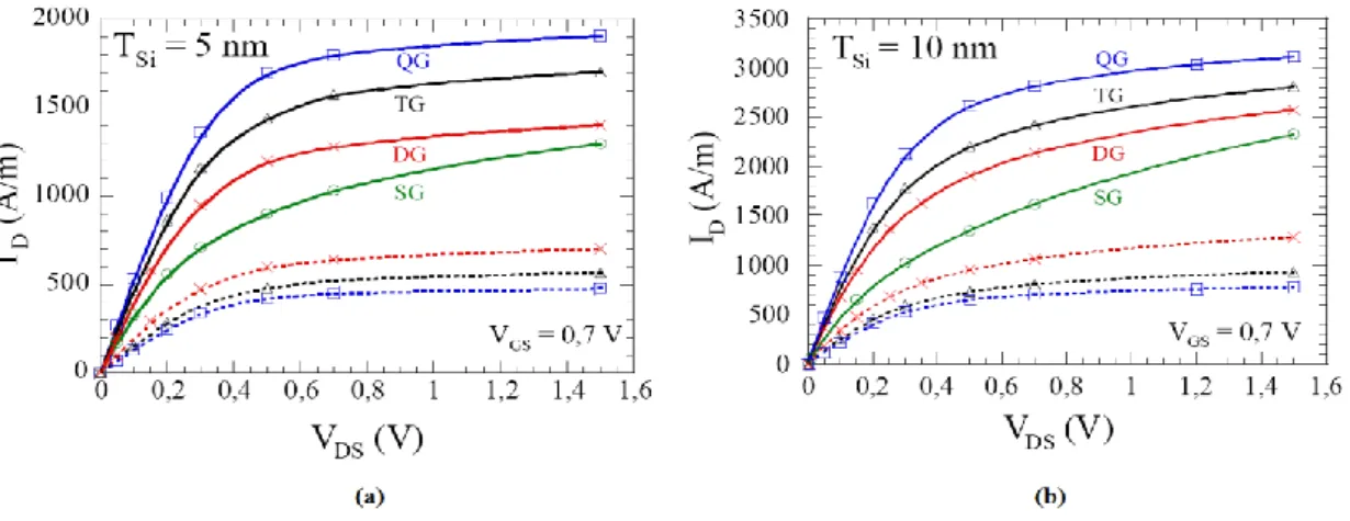
I.26. 𝐼𝐷𝑆 𝑉𝐷𝑆 characteristics of multi-gates for 𝐿 = 15𝑛𝑚, (a) 𝑡𝑠𝑖 = 5𝑛𝑚 and (b) 𝑡𝑠𝑖 = 10𝑛𝑚. In dashes, the current is divided by the number of gates; 1 for the Single Gate SOI MOSFET (SG), 2 for the double-gate (DG) MOSFET, 3 for the tri-gate (TG) MOSFET and 4 for the quadruple-Gate (QG) MOSFET. ... 32
I.27. 𝐼𝐷𝑆 𝑉𝐺𝑆 characteristics of multi-gates for 𝐿 = 15𝑛𝑚, (a) 𝑡𝑠𝑖 = 5𝑛𝑚 and (b) 𝑡𝑠𝑖 = 10𝑛𝑚. ... 32
I.28. 𝐼𝐷𝑆 𝑉𝐺𝑆 characteristics in logarithmic scale of multi-gates for 𝐿 = 15𝑛𝑚, (a) 𝑡𝑠𝑖 = 5𝑛𝑚 and (b) 𝑡𝑠𝑖 = 10𝑛𝑚. ... 33
II.1. Development history of the Soft Computing. ... 37
II.2. New design using Hybridization according to Cordon et al. ... 38
II.3: Comparison between classical and fuzzy sets. ... 43
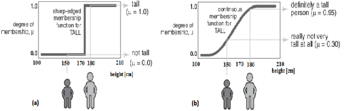
II.4. Illustration of membership functions for a set of tall people (a) crisp set (b) fuzzy set. ... 45
II.5. Triangular membership function a) general b) symmetrical. ... 45
II.6. Singleton membership function. ... 46
II.7. L membership function. ... 46
II.8: A generic form of Gamma membership function. ... 46
II.9: Gamma membership function in its linear form. ... 47
II.10. Trapezoidal membership function. ... 47
II.11. S membership function. ... 48
II.12. Gaussian membership function. ... 48
II.13. Pseudo-Exponential membership function. ... 49
II.14. Illustration of the complement (negation) of a fuzzy set. ... 49
II.15. Illustration of the union (disjunction) of two fuzzy sets. ... 50
II.16. Illustration of the intersection (conjunction) of two fuzzy sets. ... 50
II.17. Illustration of the containment (subset) between two fuzzy sets. ... 51
II.18. Block diagram of fuzzy logic model ... 52
II.19. Fuzzification step diagram. ... 53
II.20. Diagram of the rule evaluation step. ... 54
II.21. Aggregation of rule consequents step diagram. ... 55
II.22. Diagram of the defuzzification step. ... 55
II.23. Biological nervous cell (the neuron). ... 57
II.24. Artificial Neuron (Perceptron). ... 57
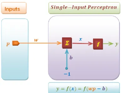
II.25. Single-Input Perceptron Model. ... 59
II.26.Multiple-Input Perceptron Model. ... 60
II.27. Transfer function: (a) hard limit; (b) linear, and (c) log-sigmoid. ... 62
II.28. A Layer of Neurons. ... 63
II.29. Single-Layer Neural Network Architecture. ... 65
II.31. Deep Neural Network Architecture. ... 66
II.32. Example of a Recurrent Network. ... 67
II.33. Example of a mesh network. ... 68
II.34. Development history of Evolutionary Computing. ... 70
II.35. Representation of the basic elements of GA. ... 72
II.36. Simple genetic algorithm flowchart. ... 74
II.37. Chromosome representation with 𝑆 parameters composed of three binary digits each. ... 75
II.38. Roulette wheel technique. ... 76
II.39. Example of cloning. ... 78
II.40. Single point crossover. ... 78
II.41. Example of multi-point crossover with two crossover points. ... 79
II.42. Uniform crossover. ... 79
II.43. Example of Arithmetic crossover. ... 80
II.44. Mutation operator. ... 80
II.45. Auxiliary hybrid system with Fuzzy Logic and ANN. ... 84
II.46. Fuzzy Logic and ANN working in a hierarchal manner. ... 84
II.47. Emerging Fuzzy Logic and ANN techniques: (a) Neuralizing the Fuzzy Logic (b) Fuzzifying ANN. ... 85
III.1. Cross-sectional view of (a) DGJL MOSFET without extensions and gate material engineering (b) DGJL MOSFET with extensions and gate material engineering. ... 90
III.2: Variation of the drain current as a function of the drain voltage (Nd=5.1018cm−3, Next=5×1019 cm−3, tsi=10 nm, tox=5 nm, L=100 nm, L1 = L2 = L/2,
M15.1eV eV M2 4.5
). ... 98III.3: Transfer characteristics Ids(Vgs) in linear scales (Vds=1.5V, Nd=5.1018 cm−3, Next=5×1019 cm−3, tsi=10 nm, tox= 5 nm, L=10 nm, L1 = L2= L/2, ). ... 99 eV M15.1 eV M2 4.5
III.4: Variation of the ON-current as a function of the channel thickness (Nd=5×1018 cm−3,
Next=5×1019 cm−3, tox=5 nm, L=100 nm, L1=L2=L/2, Vds = 2 V, Vgs = 2 V, ,
) ... 100 III.5: Variation of gain and transconductance as a function of the channel thickness (Nd=5×1018 cm−3, Next=5×1019 cm−3, tox=5 nm, L=100 nm, L1=L2=L/2, Vgs = 2 V, Vds = 2
V, , ) ... 101 III.6: Variation of the Cut-off frequency versus the channel thickness (Nd=5×1018 cm−3,
Next=5×1019 cm−3, tox=5 nm, L=100 nm, L1=L2=L/2, Vgs = 2 V, Vds = 2 V, ,
) ... 102 III.7. Evolution of the normalized overall objective function versus the number of generation of conventional DGJL MOSFET. ... 103 III.8. Evolution of the normalized overall objective function versus the number of generation of DGJL MOSFET with extensions and gate material engineering. ... 103 IV.1. Longitudinal cross sections showing the doping profile in: (a) conventional DG MOSFET, (b) Junctionless DG MOSFET. ... 112 IV.2. Relative degradation of the swing factor as function of the interfacial traps density for both cases: Junctionless and conventional DG MOSFETs. ... 113 IV.3. Relative degradation of the threshold voltage as function of the interfacial traps density for both cases: Junctionless and conventional DG MOSFETs. ... 114 IV.4. 3D view of (a) DGJL MOSFET without gate material engineering (b) DGJL MOSFET with highly doped drain/source extensions and gate material engineering. ... 118 IV.5. Common source single stage amplifier circuit. ... 119 IV.6. Voltage transfer characteristics of DGJL MOSFET based inverter circuit using conventional and improved transistors with different lengths. ... 120 IV.7. Bode plot of the transfer function of the single stage amplifier (a) gain curve (b) phase curve. ... 121 IV.8. Variation of static gain with respect to channel length of DGJL MOSFET based inverter circuit using conventional and proposed transistors. ... 121
eV M1 5.1 eV M2 4.5 eV M15.1 M2 4.5eV eV M1 5.1 eV M2 4.5
V.1. (a) Three dimensional (b) and (c) Cross-sectional views of GAA JL MOSFET. ... 125 V.2. Different stages of the proposed framework. ... 129 V.3. Variation of the drain current Ids as a function of the applied gate voltage for different
stress times (L=100 nm and Vds = 0.15 V). ... 130
V.4. Variation of the transconductance gm versus the applied gate voltage for different
stress times (L=100 nm and Vds = 0.15 V). ... 131
V.5. Maximum transconductance gmmax as a function of stress time (L=100 nm and
Vds = 0.15 V). ... 131
V. 6. Variation of the device lifetime as a function of channel length (Vds = 0.15 V). .... 132 V.7.Illustrative representation of the developed ANFIS with single input and three MFs. ... 133 V.8. Comparison between the predicted and simulated lifetime of the junctionless device (L=100 nm and Vds = 0.15V). ... 135 V.9.Comparison of the predicted and the numerical outcomes using the correlation plot. .. 136
List of tables
II.1. Common Activation Functions for Perceptrons 𝑦 = 𝑓(𝑥). ... 61
II.2. Comparison of fuzzy logic (FL), neural networks (NN) and genetic algorithms (GA) ... 83 III.1. Configuration parameters used for the genetic algorithm based optimization for both conventional and proposed structures. ... 105
III.2. Comparison of performance metrics obtained from our optimized JL devices with that of an IM-DG MOSFET for analog/RF applications. ... 106
IV.1: Simulation parameters of both devices. ... 115
IV.2: values associated with the configuration parameters used for both conventional and proposed structures ... 117
Related publications work
Published Journal Papers
1. E. Chebaki, F. Djeffal, and T. Bentrcia, „Two-dimensional numerical analysis of nanoscale
junctionless and conventional Double Gate MOSFETs including the effect of interfacial traps,‟
Phys. Status Solidi C, vol. 9, pp. 2041–2044, 2012.
2. T. Bentrcia, F. Djeffal, E. Chebaki, D. Arar, „Impact of the drain and source extensions on
nanoscale double-gate junctionless MOSFET analog and RF performances,‟ Mater. Sci.
Semicond. Process. vol.42, pp. 264-267, 2016.
3. E. Chebaki, F. Djeffal, H. Ferhati, and T. Bentrcia, „Improved analog/RF performance of
double gate junctionless MOSFET using both gate material engineering and drain/source extensions,‟ Superlattices and Microstructures, vol. 92, pp. 80–91, 2016
4. T. Bentrcia, F. Djeffal, E. Chebaki, „Approach for designing and modelling of nanoscale DG
MOSFET devices using Kriging metamodelling technique,‟ IET Circuits, Devices and Systems,
vol. 11, no. 6, pp. 618-623, 2017.
5. T. Bentrcia, F. Djeffal, D. Arar, E. Chebaki, „Improved Reliability Performance of Junctionless
Nanoscale DG MOSFET with Graded Channel Doping Engineering,‟ Phys. Status Solidi C, Vol. 14,
no. 10, October 2017. Conference Proceedings
1. T. Bentrcia, F. Djeffal, E. Chebaki, „ANFIS-based approach to study the subthreshold swing
behavior for nanoscale DG MOSFETs including the interface trap effect,‟ Proceedings of the
International Conference on Microelectronics, ICM, 2012.
2. T. Bentrcia, F. Djeffal, E. Chebaki, D. Arar „A Kriging framework for the efficient exploitation of
the nanoscale junctioless DG MOSFETs including source/drain extensions and hot carrier effect,‟
Materials Today: Proceedings 4 (2017) 6804–6813.
3. E. Chebaki, F. Djeffal, T. Bentrcia, „ANFIS-based Approach to Predict the Degradation-related
Ageing of Junctionless GAA MOSFET‟, To appear in Materials Today: Proceedings.
Book-chapter
1. T. Bentrcia, F. Djeffal, E. Chebaki, Advenced Materials Series, “Intelligent Nanomaterials”, 2nd edition, Chapter 12 „Multi-objective Design of Nanoscale Double Gate MOSFET Devices Using Surrogate Modeling and Global Optimization’, pp. 395-425, (Wiley-Scrivener Publishing, 2017).
Introduction:
Introduction
Since the invention of the first transistor in 1947, and that of the integrated circuit in 1958 by Jack Kilby, the progress of microelectronics has been considerable, both in terms of improving performance and increasing the complexity of the circuits leading to the decline in production costs [1]. The integration capacity in microelectronics follows an exponential evolution, with a density of microprocessor transistors doubled every 3 years [2]. This evolution, known as Moore's law [3,4], led to the fabrication of microprocessors of more than 1.9 billion transistors, and the realization of memories, whose density exceeds 1.3 Tb per square inch. Increasing the integration density and improving performance are made possible by decreasing (known also as downscaling or miniaturizing) the size of the transistors. The characteristic quantity of a transistor that distinguishes one generation of transistors from the next is the gate length. The International Technology Roadmap for Semiconductors (ITRS) [5] predicts that the channel length will attend the sub 10 nm region by the year 2018. The miniaturization of semiconductor devices is approaching fundamental physical limits. Indeed, the constant progression of CMOS components (complementary metal-oxide-semiconductor), established by the famous law of Moore, has always been respected, whether in terms of power, speed or size of the components [6]. So far, this approach has been very successful, but it is now reaching its limits. Today, transistors are approaching the ultimate physical limits, and performance is limited by the effects of leaks and those associated with reduced channel length. Three-dimensional devices are being exploited to take over the planar components, thanks to the better control that they allow for effects related to short channels [7].
Several remedy solutions have emerged to deal with the main problem of the miniaturization being the direct dependence of the electrical characteristics with respect to the controllable physical parameters. This causes many parasitic effects that change the performance and power consumption of the systems.
The electrical characterization of a device is of great importance and requires particular attention in the development of advanced Metal Oxide Semiconductor Field Effect Transistor(𝑀𝑂𝑆𝐹𝐸𝑇) based technologies. To do that, there are a huge number of techniques and parameters which can be crucial to develop the MOSFET and alleviate the effects related to short channel. Among these techniques, we can mention: (i) The choice of channel (length, thickness, profile doping, cross section shape, …), (ii) semiconductor (Si, Ge, GaAs,…), (iii) gate (number, shape, metal, polysilicon, gate engineering,
overlap,…), (iv) gate oxide (thickness, 𝑆𝑖𝑂2, High-k, …), (v) substrate doping (uniform, linear, Gaussian, …) and (vi) Source/Drain technology. All these techniques and parameters can largely determine the performance of the device. In designing smaller devices, the impact of the miniaturization on the reliability of the integrated circuits should also be taken into consideration.
However, after almost thirty years of frantic race to reduce the size of electronic components, the problems are not limited to the difficulties of realization. We are now seeing phenomena of a theoretical nature regarding the advantages offered by Complementary MOS (𝐶𝑀𝑂𝑆) technology. Among these phenomena, we have in particular the Drain Induced Barrier Lowering (𝐷𝐼𝐵𝐿), the short channel effects (𝑆𝐶𝐸𝑠), the quantum mechanical confinement, the gate tunneling current, the random fluctuation of the dopants. To overcome these difficulties, one of the solutions consisting in modifying the architecture of the components, in particular the increase of the number of gates in order to have a better control of the current-flow, seems a solution of choice for the future of microelectronics. But these devices, to be used by the designers of integrated circuits, need to be modeled in the form of compact models interpretable by circuit simulators. These compact models must be able to describe as precisely as possible the electrical behavior of the considered devices. The simulation of microelectronic components therefore requires new theories and modeling techniques such as artificial intelligence and soft computing techniques that improve the physical understanding of micro and nano devices.
The field of modeling, optimization, and simulation of microelectronic and nanoelectronic components can be considered as an important field of applications of artificial intelligence and soft computing techniques. Therefore, the study of the possibility of using artificial neural networks and soft computing techniques in the field of microelectronics, especially in the form of predictors and simulators of nanoscale components (Double Gate 𝑀𝑂𝑆𝐹𝐸𝑇, Trigate 𝑀𝑂𝑆𝐹𝐸𝑇, Gate All Around 𝑀𝑂𝑆𝐹𝐸𝑇, ...) is necessary. In this sense, both artificial intelligence and soft computing techniques are seen as an additional tool in the hands of the engineer and the researcher, rather than a substitute for more conventional methods. These tools are likely to provide answers where the analytical procedures show their limits.
Layout of the Thesis
Our dissertation work has twofold essential goals, the first one is to present the principles of soft computing techniques and their applications in the field of modeling, optimization, and simulation of nanoscale electronic components, and the second is to propose new design structures of multigate 𝑀𝑂𝑆𝐹𝐸𝑇𝑠 to study their electrical performances for analog and 𝑅𝐹 applications. To make the work clear and comprehensible, our dissertation is structured in five chapters: The first chapter presents briefly the bulk 𝑀𝑂𝑆 transistor and the problems caused by its miniaturization, then discusses the possible technological solutions to resolve these problems, thus exposes the 𝑆𝑂𝐼 technology with its emerging solutions and details the main electrical characteristics of both multi gate transistors Double Gate 𝐷𝐺 (𝑀𝑂𝑆 transistor), and Gate All Around 𝐺𝐴𝐴 (𝑀𝑂𝑆 transistor). The second chapter is devoted to soft computing techniques: it gives the principles of the four major techniques used in soft computing and in this dissertation namely Fuzzy Logic 𝐹𝐿 , Artificial Neural Network 𝐴𝑁𝑁 , Genetic Algorithm 𝐺𝐴 and a hybrid soft computing which is Adaptive Neuro-Fuzzy Inference System 𝐴𝑁𝐹𝐼𝑆 .
In the third chapter, we propose a new Double Gate Junctionless 𝐷𝐺𝐽𝐿 𝑀𝑂𝑆𝐹𝐸𝑇 design based on both gate material engineering and highly doped drain/source extensions. Analytical models for the long channel device associated to the drain current, analog and radio-frequency 𝑅𝐹 performance parameters are developed incorporating the impact of dual-material gate engineering and two highly doped extension regions on the 𝑎𝑛𝑎𝑙𝑜𝑔/ 𝑅𝐹 performance of 𝐷𝐺𝐽𝐿 𝑀𝑂𝑆𝐹𝐸𝑇. The transistor performance figures-of-merit (𝐹𝑜𝑀), governing the analog/RF behavior, have also been analyzed. The 𝑎𝑛𝑎𝑙𝑜𝑔/𝑅𝐹 performance is compared for the proposed design and a conventional 𝐷𝐺𝐽𝐿 𝑀𝑂𝑆𝐹𝐸𝑇 of similar dimensions, where the proposed device shows excellent ability in improving the 𝑎𝑛𝑎𝑙𝑜𝑔/𝑅𝐹 performance and provides higher drain current and improved figures-of-merit with respect to the conventional 𝐷𝐺𝐽𝐿 𝑀𝑂𝑆𝐹𝐸𝑇. Moreover, the developed analytical models are aggregated to form a mono-objective function in order to optimize the device 𝑎𝑛𝑎𝑙𝑜𝑔/𝑅𝐹 performance using Genetic Algorithms (𝐺𝐴𝑠). In comparison with the reported numerical data for Inversion-Mode (𝐼𝑀) 𝐷𝐺 𝑀𝑂𝑆𝐹𝐸𝑇, our optimized performance metrics for 𝐽𝐿 device exhibit enhancement over the reported data for 𝐼𝑀 device for the same channel length. Chappter IV is divided into two main parts: Part 1 deals with the immunity behavior of the junctionless 𝐷𝐺 𝑀𝑂𝑆𝐹𝐸𝑇 device against the hot
carrier degradation effect and we demonstrate that the junctionless 𝐷𝐺 𝑀𝑂𝑆𝐹𝐸𝑇 can be a viable option to enhance the immunity performances of nanoscale CMOS-based devices technology for nanoelectronics digital applications. In part 2, using the developed model of the Junctionless 𝐷𝐺 𝑀𝑂𝑆𝐹𝐸𝑇 in chaper III, and in order to analyze the characteristics and circuit performance of the device, we have adopted mixed mode simulation under ATLAS-2D environment for the implementation of the inverter circuit. Based on the numerical outcomes, satisfactory results are recorded in comparison with the conventional junctionless structure. The last chapter covers the applicability and the efficiency of adaptive neuro-fuzzy inference system 𝐴𝑁𝐹𝐼𝑆 approach as a predictor of junctionless gate all around (JL-GAA) 𝑀𝑂𝑆𝐹𝐸𝑇 device lifetime. Our predictions are compared versus the numerical results obtained by ATLAS simulator, where a good agreement is obtained.
Finally, we conclude this dissertation and give an overview of perspectives that can be developed to better understand this subject and also can be used in our future research.
Chapter I:
MOSFET
Transistor: miniaturization limits and
solutions
I.1 Introduction
It was in 1960 that Kahng and Attala introduced the first silicon 𝑀𝑂𝑆 transistor using an insulated gate whose gate dielectric was silicon oxide 𝑆𝑖𝑂2. Silicon was a very wise choice. It is the most abundant element of the earth's crust, after oxygen. In addition, its oxide is not only a very good electrical insulator, but it has also proved perfectly suitable for forming so-called passivation layers protecting the circuits, remarkably increasing their reliability.
𝑀𝑂𝑆 transistors on Silicon, simpler and cheaper than their bipolar competitors, but intrinsically less efficient with equivalent technological generation, flourished in the 70s and 80s due to the 𝐶𝑀𝑂𝑆 technology invented in 1968 which consumes a very small amount of energy. Since then, not only the applications in 𝐶𝑀𝑂𝑆 logic but also the memories that constitute the other major application of 𝑀𝑂𝑆𝐹𝐸𝑇𝑠 have benefited from a very strong and continuous increase in their speed and their integration density.
In 1967, Dennard invented Dynamic Random Access Memory (𝐷𝑅𝐴𝑀) by combining a 𝑀𝑂𝑆𝐹𝐸𝑇 transistor and a storage capacity. The year 1971 was the year of the design of the first microprocessor by Hoof et al of the company Intel. It is a 4 − 𝑏𝑖𝑡 processor 𝐼𝑛𝑡𝑒𝑙 4004 3𝑚𝑚 by 4𝑚𝑚 with 2250 transistors and was manufactured with Intel‟s 10µm PMOS technology [8]. The die map of the Intel 4004 processor and Intel Core i9 − 7980XE processor are illustrated in Figure I.1a and Figure I.1b, respectively.
Figure I.1: Illustration of the die map of: (a) 𝐼𝑛𝑡𝑒𝑙 4004 processor (b) 𝐼𝑛𝑡𝑒𝑙 𝐶𝑜𝑟𝑒 𝑖9 − 7980𝑋𝐸 processor [8].
Since then, many other new technologies have allowed, without really changing the manufacturing methods to reduce the size of the transistors and thus the density of the memories and the power of the microprocessors.
Till 2011, Intel for the first time used a new manufacturing process, which is the 3 dimensions (3D) mixed with multi-gate (tri-gate) designs instead of the planar manufacturing to produce the 22 nm tri-gate 3D transistor. This race for miniaturization using 3D manufacturing allows today to design transistors with 3D tri-gate and a length of 14 𝑛𝑚. This makes it possible to design processors such as the 𝐶𝑜𝑟𝑒 𝑖9, as illustrated in Figure I.1b [8] which shows the 𝐼𝑛𝑡𝑒𝑙 𝐶𝑜𝑟𝑒 𝑖9 − 7980𝑋𝐸 processor die map.
I.2 Description of the MOS transistor I.2.1 Structure of the MOS transistor
Before presenting the equations allowing the calculation of the drain current of the MOS transistor, it is necessary to define the different used notations [9].
The N-channel MOS transistor ( 𝑜𝑟 𝑀𝑂𝑆𝐹𝐸𝑇 for Metal Oxide Semiconductor Field Effect Transistor) is a quadrupole device consisting of a conductive layer (metal or highly doped polysilicon) called a gate electrode (G), a source (S ), a drain (D) and a semiconductor substrate (B) on which we locate a thin layer of insulating oxide 𝑆𝑖𝑂2 of thickness 𝑡𝑜𝑥. This is illustrated in Figure I.2.
Figure I.2: N-type MOS transistor: (a) perspective view, (b) cross-section.
The length of the transistor, denoted 𝐿, corresponds to the length of its gate (slightly overlaps the source and drain regions) and its width is denoted W. The region between the
source and drain junctions is called the channel region and is defined by its length 𝐿 and its width 𝑊. We will consider later a surface channel transistor, that is to say whose conduction is provided by the minority carriers of the substrate (electrons in the case of 𝑛𝑀𝑂𝑆𝐹𝐸𝑇), at the interface between the gate dielectric and the substrate.
Note that the 𝑀𝑂𝑆𝐹𝐸𝑇 has two additional electrodes with respect to the 𝑀𝑂𝑆 capacitance, which consist of two 𝑛+ doped caissons for an 𝑛𝑀𝑂𝑆. Thus, many properties of the 𝑀𝑂𝑆 transistor derive from those of the 𝑀𝑂𝑆 capacitor.
I.2.2 Principles operating regimes
The operating principle of the 𝑀𝑂𝑆 transistor 𝑜𝑟 𝑀𝑂𝑆𝐹𝐸𝑇 is based on the modulation of a carrier density of a semiconductor zone by an electric field perpendicular thereto. This electric field is applied by the control electrode (the gate) through an insulator (gate dielectric). The carriers created are mobile charges: electrons in the case of 𝑛𝑀𝑂𝑆 transistor, holes in the case of 𝑝𝑀𝑂𝑆 transistor. When the applied voltage to the gate 𝑉𝑔 is greater than a threshold voltage denoted 𝑉𝑡, these mobile charges constitute a conduction channel between the source and the drain. When a potential difference 𝑉𝑑𝑠 is applied between the source and the drain, the abundant carriers (source side, conventionally) are collected by the drain in the form of a current. We speak of 𝑛𝑀𝑂𝑆 transistor when the substrate is doped with acceptor type atoms and the minority carriers are the electrons. In this case, the source and drain regions are heavily doped with donor-type atoms (conduction provided by electrons). In contrast, 𝑝𝑀𝑂𝑆 transistor has a substrate doped with donor atoms and the minority carriers are the holes. Thus, macroscopically, the 𝑀𝑂𝑆 transistor behaves as a device regulating the current between two electrodes by a voltage control.
Remembering that there are three particular regions namely accumulation, depletion, and inversion and two transition points values of the 𝑉𝑔 voltage, which are flat-band voltage Vfb and threshold voltage Vt as illustrated in Figure I.3 for the n-type 𝑀𝑂𝑆𝐹𝐸𝑇 device.
Figure I.3: Energy band diagrams of an n-type 𝑀𝑂𝑆 transistor [10].
Notice that downward arrows indicate positive 𝑉𝑔 whereas upward arrows present negative 𝑉𝑔.
The flat-band voltage is given by: Vfb = g −S − Qox
Cox (I.1)
where 𝑔 and 𝑆 are the gate and the substrate work functions respectively and 𝑄𝑜𝑥 is the charge at the 𝑆𝑖 − 𝑆𝑖𝑂2 interface. The gate voltage in excess of Vfb is divided between the substrate, the oxide and the poly-gate depletion layer.
Vg = Vfb+𝑆+ Vox +𝑝𝑜𝑙𝑦 (I.2)
Vg = Vfb +𝑆−𝑄𝑠𝑢𝑏
𝐶𝑜𝑥 +𝑝𝑜𝑙𝑦 (I.3)
where 𝑆 is the surface potential, or the substrate band bending and Vox is the oxide voltage. The quantity 𝑄𝑠𝑢𝑏(𝐶/𝑐𝑚2) is the sum of the accumulation, inversion, and depletion-layer charges.
At the threshold of inversion, 𝑆 and Vt are expressed in terms of 𝐵 and Vfb respectively
𝑆𝑡 = ±2𝐵 (I.4)
𝐵 =𝑘𝑇 𝑞ln
𝑁𝑠𝑢𝑏
Vt = Vfb +𝑆𝑡± q Nsub2 εs/ st
Cox (I.6)
The important parameters of the transistor are given below:
The threshold voltage 𝑉𝑡 is the gate voltage needed to form a conduction channel (inverting layer) between the source and the drain. The typical threshold voltage of a nano MOSFET is less than 0.4 V.
The transconductance or gain 𝑔𝑚 is defined by:
𝑔𝑚 = 𝜕𝐼𝑑𝑠 𝜕𝑉𝑔𝑠 𝑉
𝑑𝑠=𝑐𝑡𝑒
(I.7)
and must be as high as possible. The transconductance increases very rapidly when the channel length becomes less than 100 nm.
The output conductance (𝑔𝑑𝑠) is given by:
𝑔𝑑𝑠 = 𝜕𝐼𝑑𝑠 𝜕𝑉𝑑𝑠 𝑉
𝑔𝑠=𝑐𝑡𝑒
(I.8)
The subthreshold slope (𝑆𝑆): it represents the gate voltage to be applied (under the threshold voltage value) to increase the drain current by one decade:
𝑆𝑆 = 𝑑𝑉𝑔𝑠/𝑑(𝑙𝑜𝑔 𝐼𝑑𝑠) (I.9)
I.2.2.1 Linear operating regime
The total current near the 𝑆𝑖 − 𝑆𝑖𝑂2 interface is the sum of the diffusion and drift currents of the free carriers. In inversion, we consider that the majority concentration is zero in the channel and we can write [11]:
x y q nn Dn n Jn J , (I.10)where 𝑛 is the mobility of the electrons in a weak field in the inversion layer, 𝐷𝑛 the electron diffusion coefficient and n the concentration gradient. If we consider Shockley's gradual approximation [12], i.e when the transistor is operating in unsaturated mode or when the channel is not pinched, we consider that the field lines are parallel to the interface, (I.10) becomes:
2 1 J x n J x n n q n qD grad n J
(I.11)with 𝑥 being the field along the 𝑥 axis (Figure I.3), 𝑗1 is the drift component (due to the electric field) and 𝑗2 represents the diffusion current.
Considering the Einstein coefficient 𝐷𝑛 = 𝑛 𝑘𝑇
𝑞 where 𝑛 is the mobility of the electrons supposed constant, and knowing that 𝑥 derives from a scalar potential expressed by:
𝑥 = −𝑔𝑟𝑎𝑑( 𝑐 )), the equation (I.11) can be simplified to [11]:
dx
d
n
q
J
c n n
(I.12)where the potential relationships are given by:
G
BS c BS DS G c BS cV
x
V
L
x
V
V
L
x
V
x
0
0
The total current is obtained by integrating the density Jn over the entire thickness of the
inverting layer 𝑦𝑖 of the transistor of width 𝑊𝐺:
0 0 0 i i i y y c n G c n G y n G DSndy
dx
d
W
dy
dx
d
n
q
W
dy
J
W
I
(I.13)Moreover, since 𝐼𝐷𝑆 being constant all along the channel, it comes that:
BS DS BS G V V V n c n G G DS LI
DSdx
I
L
W
Q
d
0 (I.14) where
0 i y nndy
Q
.On the other hand, the influence of 𝑉𝐵𝑆 being identical at all points of the channel on the free carrier concentrations, the equation (I.14) can be rewritten:
DS VDS D SC G n V n G n DSQ
Q
V
dV
L
W
dV
V
Q
L
W
I
0 0
(I.15)The charge 𝑄𝑆𝐶 can be considered as the total charge of the semiconductor to which the 𝑄𝐷 charge of the depleted area under the inversion zone must be subtracted.
F OX OX ms c GS OX SCC
Q
V
C
Q
2
(I.16)
c BS F
Si A DN
V
Q
2
2
(I.17)To obtain the expression of 𝐼𝐷𝑆, it is necessary to substitute equations (I.16) and (I.17) in equation (I.15), the current 𝐼𝐷𝑆 is then rewritten in the simplified form:
1/2 1/2 2 2 1 2 1 2 2 DS BS F V F BS F FB GS DS OX n G G DS C V V V V V V L W I th (I.18)which makes it possible to express the drain current of a MOS transistor in linear mode in the following form:
DS DS th GS OX n G G DS
C
V
V
V
V
L
W
I
2
(I.19)I.2.2.2 Saturation operating regime
As the drain voltage increases, the depletion width expands and reduces the inversion charge at the edge of the drain. The transistor goes into saturation mode when 𝑉𝐷𝑆 is large enough that 𝑄𝑖𝑛𝑣 (x = 𝐿𝑒𝑓𝑓) is almost zero. This occurs for 𝑉𝐷 equals to 𝑉𝐷𝑠𝑎𝑡. Then, we have:
T GS DsatV
V
V
(I.20)There is another approach to determine the saturation drain voltage. It is enough to consider that for 𝑉𝐷𝑆 > 𝑉𝐷𝑠𝑎𝑡 the drain current does not vary anymore (ideal case), which leads to solve: sat DS V DS DS d V I G (I.21)
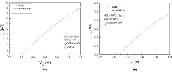
2 2 T GS OX n G G DS V V C L W I sat (I.22)Figures I.4a, I.4b, I.5a and I.5b [13] show the calculated 𝐼𝐷𝑆 𝑉𝐺𝑆 and 𝐼𝐷𝑆(𝑉𝐷𝑆) characteristics (using equations (I.19) and (I.22)) and measured for a long-channel transistor (𝑊𝐺 / 𝐿𝐺 = 10/10μm) and a short-channel transistor (𝑊𝐺 / 𝐿𝐺 = 10/0.13μm). There can be a discrepancy between the model and the measurement when the gate and the drain voltages increase. On small geometries, the gap is accentuated, which highlights the need to refine the equations including the effects related to the reduction of the dimensions of the MOSFET transistors. In the next section, we will present these effects, starting from their physical origins, to arrive at a mathematical quantification allowing including their impacts on the electrical behavior of the devices. We will in particular describe the reduction of the carrier mobility in the channel under the influence of the electric field, the modulation of the channel length related to the extension of the depletion width of the Drain-Substrate junction.
Figure I.4: Comparison between modeling and measurement of linear drain current for a MOS transistor with ultra thin oxide Tox = 2.1nm (a) MOS with long N- type channel
(Weff/Leff = 10/10μm) and (b) MOS with short N- type channel (Weff/Leff = 10/0.13μm)
Figure I.5: Comparison between modeling and drain current measurement vs. drain voltage for different gate voltage values for a MOS transistor with ultra thin oxide Tox =
2.1nm (a)MOS with long N- type channel (Weff/Leff = 10/10μm) and (b) MOS with short
N- type channel (Weff/Leff = 10/0.13μm) [13]
I.3 Presentation of SOI technology I.3.1 SOI technology with a single gate
In SOI (Silicon On Insulator) technology, unlike the bulk MOSFET (Figure I.6a) where the components are made on a silicon substrate - sometimes called bulk - with a thickness of the order of 600 μm of which only the first microns on the surface are really useful, the SOI is realized on a Silicon film previously placed on a buried oxide layer (Figure I.6b) [14]. The silicon film has a thickness noted by 𝑡𝑆𝑖 .
In an opposite manner of the bulk MOS transistor for which the inversion channel is located at the silicon-oxide interface, the SOI structure gave rise to the concept of volume inversion [15]. The presence of the buried oxide allows a better control of the potential in the channel by the gate compared to the MOS transistor on silicon.
Figure I.6: Cross-section Schematic view of MOS transistors (a) bulk and (b) SOI.
For thick silicon films, the depletion zone in the film does not reach the buried oxide; we then speak of the partially depleted transistor (or PDSOI). When the thickness of the film is reduced and the depletion reaches the buried oxide, the film is completely depleted and the gate improves the control of the potential in the film; we are talking about a fully depleted transistor (or FDSOI). Figure I.7 describes these two structures.
Figure I.7: Schematic representation of a SOI transistor: (a) fully depleted and (b) partially depleted.
The fact that the SOI is partially or fully depleted depends essentially on the extension of the depleted layer in the silicon film. The depth 𝑥𝑆𝑖 of the depletion zone in the film will depend on the doping of the film [16].
I.3.1.1 Advantages of SOI compared to bulk MOSFET
The electrical properties of this structure, in particular, the completely depleted SOI transistor, are in general much better compared to the bulk MOS transistor [17]. It is also
considered that this component is a potential candidate to successfully integrate devices of longitudinal dimensions less than or equal to 30 nm [17]. We will now see the main properties of the SOI technology compared to the bulk MOSFET.
The advantages of SOI technology are multiple including: Decrease of parasitic effects
Just by the presence of buried oxide, parasitic capacitances are considerably reduced.
The source-substrate and drain-substrate junction capacitances, which correspond to the capacity of a reverse-biased junction for the bulk MOSFET, are actually present by a unique oxide capacitor 𝐶𝐵𝑜𝑥 for the SOI MOSFET.
The SOI transistor has, still in comparison with the bulk MOS transistor, a thinner and isolated conduction channel [17] besides a simplification of the interconnection levels above the transistors due to the absence of the boxes.
When the silicon film is weakly doped, or even undoped, it can be completely depleted at zero gate voltage, which is also advantageous with regard to the surface leakage current.
On the SOI (Figure I.7b), these zones are totally isolated and thus the breakdown between these two zones is very difficult.
The ability to increase the integration density is a direct consequence of suppressing this parasitic effect [15].
Improved gate control over the depletion charge.
Charge separation models provide the proportion of the depletion charge controlled by the gate relative to that controlled by the source and drain.
The ratio between the depletion charge controlled by the gate and the drain (or the source) is much greater for the SOI transistor, compared to bulk MOS transistor, with identical dimensions (L, W, 𝑡𝑜𝑥, 𝑋𝑗).
This phenomenon is more pronounced as the length of the channel decreases as shown in Figure I.8.
Figure I.8: Distribution of the depletion charge for bulk MOSFET and SOI [18].
Improvement of the subthreshold slope The subthreshold slope is defined by: 𝑆𝑆 = 𝑛 ln(10)𝑘𝑇
𝑞 (I.23)
with 𝑛 = 1 + (𝐶𝑑𝑒𝑝/𝐶𝑜𝑥) is the substrate factor.
Figure I.9: Capacitive equivalent circuit (a) of a bulk MOSFET and (b) of a SOI [19].
For the bulk MOS transistor (Figure I.9a), since 𝐶𝑑𝑒𝑝 is not negligible, this implies that n> 1. On the other hand, for the SOI transistor on thin film, the entire film is depleted before the voltage reaches the threshold value and therefore 𝐶𝑆𝑖 is a constant, hence:
10 ln e nkT SS (I.24) where 2 1 2 1 1 1 OX Si OX Si OX Si OX Si C C C C C C C C n 𝐶𝑆𝑖 denotes the capacity of the completely depleted silicon film and 𝐶𝑜𝑥 1 and 𝐶𝑜𝑥 2, the oxide capacities located respectively in the upper part and the lower part of the silicon film. In Figure I.9b, 𝑆1 and 𝑆2 denote the surface potentials in the upper and lower regions of the film respectively and, finally, 𝑉𝐺1 and 𝑉𝐺2 correspond to the gate polarizations, always in the upper region and the lower region of the film.
Usually, for thin films we have 𝐶𝑜𝑥 2 𝐶𝑜𝑥 1 and 𝐶𝑜𝑥 2 𝐶𝑆𝑖, we get in this case a value of n close to unity and an optimal subthreshold slope. The subthreshold slope at the room temperature is practically minimal (= 60 mV / dec for n = 1) in SOI technology (Figure I.10).
Figure I.10: Comparison of the subthreshold slope of the MOS transistor in bulk and SOI technologies, for a constant geometry [17].
I.3.1.2 Major disadvantage of SOI technology
The advantages of SOI technology are numerous. However, their major disadvantage, especially with regard to PDSOI, is the significance of the short channel effects (Figure I.11). The polarization of the drain can induce short channel effects by electrostatic influence through the buried oxide. This harmful effect becomes significant especially when the thickness of the oxide is important.
Figure I.11: Electrostatic influence on SOI with single gate [17].
Naturally, reducing the oxide thickness would only reduce the electrostatic influence; however, inserting a gate below the oxide would be a shield that allows completely blocking the field lines. This may directly protect the channel and reduce the short channel effects. Such structure is called Double-Gate (DG) and comes within the framework of multi-Gate structures to be presented in the following section.
I.3.2 Multi-gate transistors
The SOI technology with a single gate does not make it possible to reduce the short-channel effects due in particular to the electrostatic influence. However, the addition of a gate around the silicon layer not only promotes the isolation of the conduction channel and implicitly its protection, but also offers better control over this channel. As a result, SOI structures appear with two, three, or even four gates [17].
The evolution of the SOI devices with the increase of the gates number is illustrated in Figure I.12 and Figure I.13.
Depending on the number of gates controlling the channel and their positioning around the silicon film, the SOI MOSFET denomination differs. So, we find in the literature:
Figure I.12: Evolution of SOI technology over the years [17-18] [20].
Double-Gate structure: The double-gate MOS transistor (DG) consists of two gates placed on the horizontal plane. Figure I.13 shows the architecture in which each gate has control over the channel(s).
Figure I.13: Single gate versus various multi-gate structures: (a) Single-Gate SOI, (b)Double-Gate SOI, (c) Tri-Gate SOI, (d) Π Gate, (e)Quadruple-Gate SOI, (f)
![Figure I.8: Distribution of the depletion charge for bulk MOSFET and SOI [18].](https://thumb-eu.123doks.com/thumbv2/123doknet/14897588.652214/38.892.187.720.115.322/figure-i-distribution-depletion-charge-bulk-mosfet-soi.webp)
![Figure I.10: Comparison of the subthreshold slope of the MOS transistor in bulk and SOI technologies, for a constant geometry [17]](https://thumb-eu.123doks.com/thumbv2/123doknet/14897588.652214/39.892.254.651.423.747/figure-comparison-subthreshold-slope-transistor-technologies-constant-geometry.webp)
![Figure I.12: Evolution of SOI technology over the years [17-18] [20].](https://thumb-eu.123doks.com/thumbv2/123doknet/14897588.652214/41.892.216.688.116.481/figure-i-evolution-soi-technology-years.webp)
![Figure II.2: New design using hybridization according to Cordon et al.[86].](https://thumb-eu.123doks.com/thumbv2/123doknet/14897588.652214/59.892.220.694.657.1033/figure-ii-new-design-using-hybridization-according-cordon.webp)