Publisher’s version / Version de l'éditeur:
Applied Physics Letters, 83, 13, pp. 2638-2640, 2003-09-29
READ THESE TERMS AND CONDITIONS CAREFULLY BEFORE USING THIS WEBSITE. https://nrc-publications.canada.ca/eng/copyright
Vous avez des questions? Nous pouvons vous aider. Pour communiquer directement avec un auteur, consultez la première page de la revue dans laquelle son article a été publié afin de trouver ses coordonnées. Si vous n’arrivez pas à les repérer, communiquez avec nous à PublicationsArchive-ArchivesPublications@nrc-cnrc.gc.ca.
Questions? Contact the NRC Publications Archive team at
PublicationsArchive-ArchivesPublications@nrc-cnrc.gc.ca. If you wish to email the authors directly, please see the first page of the publication for their contact information.
NRC Publications Archive
Archives des publications du CNRC
This publication could be one of several versions: author’s original, accepted manuscript or the publisher’s version. / La version de cette publication peut être l’une des suivantes : la version prépublication de l’auteur, la version acceptée du manuscrit ou la version de l’éditeur.
For the publisher’s version, please access the DOI link below./ Pour consulter la version de l’éditeur, utilisez le lien DOI ci-dessous.
https://doi.org/10.1063/1.1608488
Access and use of this website and the material on it are subject to the Terms and Conditions set forth at
Interfacial growth of HfOxNy gate dielectrics deposited using
[(C2H5)2N]4Hf with O2 and NO
Lee, M.; Lu, Z. -H.; Ng, W. T.; Landheer, D.; Wu, X.; Moisa, S.
https://publications-cnrc.canada.ca/fra/droits
L’accès à ce site Web et l’utilisation de son contenu sont assujettis aux conditions présentées dans le site LISEZ CES CONDITIONS ATTENTIVEMENT AVANT D’UTILISER CE SITE WEB.
NRC Publications Record / Notice d'Archives des publications de CNRC:
https://nrc-publications.canada.ca/eng/view/object/?id=8d472442-7a67-495a-8d2d-aeee49a23014 https://publications-cnrc.canada.ca/fra/voir/objet/?id=8d472442-7a67-495a-8d2d-aeee49a23014Interfacial growth in HfO
xN
ygate dielectrics deposited using †„C
2H
5…
2N‡
4Hf
with O
2and NO
M. Leea)and Z.-H. Lu
Department of Materials Science and Engineering, University of Toronto, Toronto, Ontario M5S 3E4, Canada
W.-T. Ng
Department of Electrical and Computer Engineering, University of Toronto, Toronto, Ontario M5S 3E4, Canada
D. Landheer, X. Wu, and S. Moisa
Institute for Microstructural Sciences, National Research Council of Canada, Ottawa, Ontario K1A 0R6, Canada
~Received 5 May 2003; accepted 21 July 2003!
The interface growth by oxygen diffusion has been investigated for 5 nm thick HfOxNygate-quality
dielectric films deposited on Si~100! by low-pressure pulsed metalorganic chemical vapor deposition. Analysis by x-ray photoelectron spectroscopy of the films deposited using the precursor tetrakis ~diethylamido! hafnium with O2 showed that the films contained 4 at. % nitrogen. This
increased to 11 at. % N when NO was used as the oxidant. Significant growth of the interface layer was observed for films exposed to air at ambient temperature and lower rates of growth were observed for vacuum annealed films and those with the higher N content. For films annealed in O2
at temperatures in the range 600–900 °C, the activation energies of the interfacial growth were 0.36 and 0.25 eV for N concentrations of 11 and 4 at. %, respectively. The results were interpreted in terms of atomic oxygen formation in the bulk and reaction at the interface. The increase in N incorporation from 4 to 11 at. % increases the crystallization temperature from between 500 and 600 °C to between 600 and 700 °C. © 2003 American Institute of Physics.
@DOI: 10.1063/1.1608488#
Hafnium oxide has proven to be one of the most prom-ising candidates to replace SiO2 as the gate insulator in
sub-0.1-mm complementary metal oxide semiconductor ~CMOS! devices due to its relatively high dielectric constant and ther-modynamic stability when in direct contact with Si.1,2 How-ever, the high oxygen diffusion rate through hafnium oxide,3 which results in the ready formation of interface layers, and a low crystallization temperature4 remain concerns. The in-corporation of Si to form silicates with a higher crystalliza-tion temperature has been investigated but silicon/hafnium ratios as high as 9 may be required,5resulting in a significant reduction in the dielectric constant over that of pure HfO2.
The incorporation of N rather than Si may ultimately result in a better tradeoff between dielectric constant and crystalli-zation temperature. Even low concentrations of nitrogen may significantly reduce the diffusion of B or the formation of an interface layer when MOS structures are exposed to oxygen.6 In this letter, hafnium oxynitride films deposited by met-alorganic chemical vapor deposition ~MOCVD! using the amide precursor tetrakis ~diethylamido! hafnium ~TDEAH!, @(C2H5)2N#4Hf, are described. The growth of an interfacial
layer during air exposure and after annealing in O2 was
ana-lyzed by x-ray photoelectron spectroscopy ~XPS! and trans-mission electron microscopy ~TEM!.
p-type Si~100! substrates with a resistivity of 0.01–0.02
V cm were given a HF-last RCA clean just prior to their
introduction into an ultrahigh vacuum system which com-prises a low-pressure MOCVD system, an in situ XPS sys-tem, and a rapid postdeposition annealing ~PDA! chamber. A 0.1 M solution of TDEAH dissolved in the octane was intro-duced with Ar carrier gas into the CVD chamber with the vaporizer and gas distribution system held at 150 °C. Si sub-strates were held at a temperature of 400 °C during deposi-tion, and the oxidant gas, either O2 or NO, was introduced
into the CVD chamber at a pressure of 11 mTorr through a separate gas introduction ring. The oxidant was introduced for 5 min prior to film deposition with the substrate held at 500 °C, resulting in the formation of a buffer layer. XPS showed these films to be ;0.4 nm thick with the approxi-mate composition of SiO2 or SiON, depending on whether
the oxidant was O2 or NO, respectively. Separate precursor
and oxidant pulses were employed during the deposition of 5 nm thick films with intervening nitrogen flushing steps to minimize carbon contamination. XPS analysis was per-formed in situ with all peaks referenced to the Si 2 p sub-strate peak at 99.4 eV.
Figure 1~a! shows the N 1s XPS spectrum of a film de-posited using NO as the oxidant. The peak at 396.0 eV was attributed to N–Hf bonds in the bulk of the film @the N 1s (N–Hf) peak#. Since the films were relatively thick, the peak at 398.3 eV was attributed to N–C bonds7 @the N 1s (N–C) peak# arising from residual precursor on the surface rather than N–Si bonds at the interface. Most of the N 1s (N–C) peak vanished after mild sputtering in an ex situ XPS system. As shown in Fig. 1~b!, the O 1s peak could also
a!Electronic mail: minsoo.lee@utoronto.ca
APPLIED PHYSICS LETTERS VOLUME 83, NUMBER 13 29 SEPTEMBER 2003
2638
0003-6951/2003/83(13)/2638/3/$20.00 © 2003 American Institute of Physics
be fitted with two peaks, the O 1s (O–Si) component at 532.4 eV attributed to oxygen bonded to Si in an interfacial layer, and the O 1s (O–Hf) peak at 530.5 eV due to oxygen bonded to Hf in the deposited layer. Using standard sensitiv-ity factors for the O 1s (O–Hf), N 1s (N–Hf), and Hf 4 f peaks, the average nitrogen composition was 11 at. % for the films deposited with NO gas and 4 at. % for those deposited with O2.
The existence of N–Hf bonds in the bulk of the films is also evident from the positions of the Hf 4 f7/2peak shown in the inset of Fig. 1~b!. This peak is at 17.9 eV for HfO2films
8
and 15.3 eV for HfN1.9films.9Nitrogen bonding results in a
shift to lower energy for the Hf 4 f doublet and an increase in the area ratio of the Hf 4 f7/2 and Hf 4 f5/2 components from the ideal value of 1.4, since the Hf 4 f5/2component shifts in the direction of the Hf 4 f7/2 component. The area ratio is 1.66 and 1.46 for the films deposited using NO and O2,
respectively, while the corresponding positions of the Hf 4 f7/2 peak energy are 17.0 and 17.3 eV, consistent with previous work.6
The Si 2 p peak was fitted with three components, two comprising the standard Si 2 p3/221/2 doublet from the sub-strate, and the Si 2 p ~bonded! peak due to silicon bonded at the interface. The energy separation between the substrate and bonded Si peaks, DSi 2 p, was lower for the films depos-ited with NO ~2.5 eV! than the ones deposdepos-ited with O2 ~3.1
eV!. This indicates the presence of N at the interface for the former films, although the presence of Hf or suboxide bond-ing near the interface cannot be ruled out.
Figure 2~a! shows XPS spectra of the Si 2 p peak for the films deposited using O2, after exposure to ambient air. A
significant increase of the Si 2 p(bonded) and Si 2 p(substrate) area ratio in the air-exposed samples was observed for both oxidant gas samples, accompanied by an increase of DSi 2 p to the value characteristic of that for SiO2. This indicates that interfacial reactions occurred as
previously observed in other high-k films, such as Y2O3,
La2O3, and Sc2O3.10–12 Previous research on the oxygen
diffusion through these high-k oxides suggested that the spe-cies responsible for interfacial growth was atomic oxygen released in the film from absorbed water or molecular oxygen.13 Assuming that the interfacial layer is SiO2, a
nominal interfacial layer thickness, dIL, can be obtained
from the Si 2 p(bonded)/Si 2 p(substrate) peak area ratio us-ing the parameters of Ref. 14. The increase in dIL with
ex-posure to air, DdIL, is shown in Fig. 2~b! for films deposited
using O2 and NO, with and without a 1 s in situ PDA at
800 °C in a vacuum of 131028Torr. The results show that
a higher concentration of N in the films retards growth of the interfacial layer in air. The PDA also retarded the growth of the interface layer and this can be attributed to film densifi-cation during annealing.
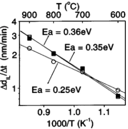
Interfacial growth during subsequent annealing in 1 atm of O2was also investigated with films deposited with O2and
NO, with and without the vacuum PDA. O2 annealing was
done at temperatures of 600, 700, 800, and 900 °C and the growth rate DdIL/Dt was determined from the change in dIL
after 1 min anneals. Arrhenius plots of the nominal interfa-cial layer thickness calculated from the XPS Si 2 p spectra are shown in Fig. 3. Linear fits of the data gave activation energies of 0.25 and 0.36 eV for the films deposited using O2
FIG. 1. ~a! N 1s and C 1s ~inset! XPS spectra of HfOxNy film deposited
with NO oxidant. The closed circles are measured data, dashed lines are fitted peaks, and solid line is the sum of all fitted peaks; ~b! corresponding O 1s and Hf 4 f spectra ~inset!.
FIG. 2. ~a! Si 2 p XPS spectra of HfOxNy film deposited using O2 after exposure to air for ~1! 20 min, ~2! three days, ~3! five days, and ~4! seven days. ~b! Increase in nominal thickness of interface layer, DdIL, with air
exposure: Closed ~open! symbols are for films with ~without! vacuum PDA: ~d!, ~s! 4 at. % N, ~j!, ~h! 11 at. % N.
2639 Appl. Phys. Lett., Vol. 83, No. 13, 29 September 2003 Leeet al.
~4 at. % N! and NO ~11 at. % N!; respectively. For the films deposited with NO there is no significant difference in acti-vation energy for the films with and without the vacuum anneal. The higher activation energy for the film deposited with NO is likely a result of N at high-k film and the inter-face, reducing oxygen diffusion and the interface reaction rate. Despite the higher activation energy, the NO-deposited films have thicker interface layer at high temperature, as a result of a larger frequency factor in Arrhenius plot. This may indicate that the N sites in the bulk are more effective at converting H2O or O2, providing more O which diffuses
rapidly to the interface.
TEM images of the films show that the increase in nitro-gen incorporation from 4 to 11 at. % increases the crystalli-zation temperature from between 500 and 600 °C to between 600 and 700 °C, in agreement with previous observations at higher N concentrations.15
In summary, HfOxNy films were deposited by MOCVD
using @(C2H5)2N#4Hf with O2 or NO as the oxidant. The
nitrogen composition of the films deposited at 400 °C has been determined to be 11 at. % with NO and 4 at. % with O2.
Interfacial growth during air exposure at room temperature
was attributed to absorption and diffusion of O2 or H2O with
subsequent formation of atomic oxygen in the high-k film. It was confirmed that nitrogen incorporation and vacuum an-nealing at 800 °C delays the interfacial growth during air exposure. Activation energies for the interfacial growth for 1 min anneals in O2 were 0.25 and 0.36 eV for films
contain-ing 4 and 11 at. % N, respectively. The vacuum anneal does not decrease interfacial layer growth during high-temperature oxygen anneals. N incorporation decreases the rate of inter-facial growth, even at these low levels, increases the crystal-lization temperature of hafnium oxide films.
The authors acknowledge T. Quance and X. Tong for their assistance in the preparation of samples. Financial sup-port from the ECAN ORDCF Award is also greatly appreci-ated.
1G. D. Wilk, R. M. Wallace, and J. M. Anthony, J. Appl. Phys. 89, 5243 ~2001!.
2
B. H. Lee, L. Kang, R. Nieh, W.-J. Qi, and J. C. Lee, Appl. Phys. Lett. 76, 1926 ~2000!.
3A. Kumar, D. Rajdev, and D. L. Douglass, J. Am. Chem. Soc. 55, 439 ~1972!.
4D. A. Neumayer and E. Cartier, J. Appl. Phys. 90, 1801 ~2001!. 5
G. D. Wilk, R. M. Wallace, and J. M. Anthony, J. Appl. Phys. 87, 484 ~2000!.
6C. S. Kang, H.-J. Cho, K. Onishi, R. Nieh, R. Choi, S. Gopalan, S. Krish-nan, J. H. Han, and J. C. Lee, Appl. Phys. Lett. 81, 2593 ~2002!. 7
J. F. Moulder, W. F. Stickle, P. E. Sobol, and K. D. Bomben, Handbook of X-Ray Photoelectron Spectroscopy ~Perkin-Elmer, Eden Prairie, MN, 1992!.
8C. Morant, L. Galan, and J. M. Sanz, Surf. Interface Anal. 16, 304 ~1990!. 9Y. Baba, T. A. Sasaki, and I. Takano, J. Vac. Sci. Technol. A 6, 2945
~1988!.
10B. W. Busch, J. Kwo, M. Hong, J. P. Mannaerts, B. J. Sapjeta, W. H. Schulte, E. Garfunkel, and T. Gustafsson, Appl. Phys. Lett. 79, 2447 ~2001!.
11
S. Guha, E. Cartier, M. A. Gribelyuk, N. A. Borjarczuk, and M. A. Copel, Appl. Phys. Lett. 77, 2710 ~2000!.
12G. A. Botton, E. Romain, D. Landheer, X. Wu, M.-Y. Wu, M. Lee, and Z.-H. Lu, Electrochem. Soc. Proc. 2003-02, 251 ~2003!.
13J. R. Engstrom, D. J. Bonser, and T. Engel, Surf. Sci. 268, 238 ~1992!. 14
Z. H. Lu, J. P. McCaffrey, B. Brar, G. D. Wilk, R. M. Wallace, L. C. Feldman, and S. P. Tay, Appl. Phys. Lett. 71, 2764 ~1997!.
15M. R. Visokay, J. J. Chambers, A. L. P. Rotondaro, A. Shanware, and L. Colombo, Appl. Phys. Lett. 80, 3183 ~2002!.
FIG. 3. Arrhenius plot for the growth of the nominal interfacial layer thick-ness of HfOxNy films annealed in O2 at 1 atm.: ~d!~d!~d! films with 4 at. % N deposited using O2, ~h!~h!~h! films with 11 at. % N deposited using NO, ~j!~j!~j! films with 11 at. % N vacuum annealed at 800 °C after deposition with NO.
2640 Appl. Phys. Lett., Vol. 83, No. 13, 29 September 2003 Leeet al.